SRAM BASED IN-MEMORY MATRIX VECTOR MULTIPLIER
K.G.Venkata krishna 1 , P. Hema naga sai surya kumar 2, S. Meghana 3, A. Reddy prasad reddy 4 , G. Muni jayanth 5
1 Assistant Professor, Department of Electronics and Communication Engineering, Krishna University College of Engineering and Technology Krishna University, Machilipatnam Andhra Pradesh, India
2 U.G Student, Department of Electronics and Communication Engineering, Krishna University, Machilipatnam, Andhra Pradesh, India.
3 U.G Student of Department of Electronics and Communication Engineering, Krishna University, Machilipatnam Andhra Pradesh, India
4 U.G Student of Department of Electronics and Communication Engineering, Krishna University, Machilipatnam Andhra Pradesh, India
5 U.G Student of Department of Electronics and Communication Engineering, Krishna University, Machilipatnam Andhra Pradesh, India. ***
Abstract - TheweightsstoredintheSRAMareturnedinto proportionalvoltagesusingaD/Aconverter,whichishowthe SRAM-based matrix-vector multiplier for in-memory computation functions. These voltages are subsequently multipliedbyaswitched-capacitorstageusinganm-bitdigital inputactivation.Finally,chargesharingisusedtogatherthe output voltages associated with the various multiplication outcomes along one column.
The needed circuit size, calculation time, and power consumptiongrowlinearlywiththespecifiedarchitecture.For the energy usage in switches and capacitors, analytical formulae are provided. Additionally, the effect of manufacturing mismatch on the precision of analogue computing is lookedat.
Key Words: Analog Computation, Hardware Accelerator, In-Memory Computation, SRAM, DRAM
1.INTRODUCTION
During computations, a lot of data is sent back and forth betweenthephysicallydistinctmemoryandprocessorunits of standard Von-Neumann computing systems. It is necessary to reevaluate both the well-established chargebased memory technologies, such as SRAM, DRAM, and Flash,aswellastheemergingresistance-basednonvolatile memorytechnologiesinordertogetaroundthelimitations ofthetraditionalVon-Neumann-basedarchitectures,which enforceanassertiveseparationoftheprocessingunitand thememorysubsystem.
It is becoming more and more obvious that switching to computingarchitectureswithco-locatedlogicandmemory is necessary for application domains like artificial intelligence (AI). IMC, a unique non-Von Neumann computingparadigm,usesthephysicalcharacteristicsand
dynamical state of charging resistance-based memory devices to conduct certain computations directly in the memory.AnIMC-basedsystemmaybeusedtoaccomplisha variety of computing tasks, including logical operations, arithmetic operations, and even certain machine learning activities.
1.1 Motivation
The need for low-power integrated circuits has greatly increased over the past several years as a result of the increasingexpansionofbattery-operateddevicesincluding wireless communication units, portable entertainment devices, and implementable bio-medical chips. SRAM will eventuallyaccountformorethan60%ofSoCs,predictsthe International Technology Roadmap for Semiconductors (ITRS). The problem of consuming power and space is significantly solved when the technology scales by greatly increasingthetransistordensityintheSRAMunits.
1.2 Objective
The in-memory matrix-vector multiplier built on SRAM has as its primary goal a reduction in the amount of time required to complete computations. Performance may be improved and power consumption can be decreased by utilisingSRAMtechnology.
2. LITERATURE SURVEY

2.1 Static Random Access Memory.
InSoCs,embeddedSRAMsmaytakeupthebulkofthechip space.Modernscaled-downtechnologies'increasingprocess spreadsandnon-catastrophicdefect-relatedvulnerabilityto externalfactorsmightjeopardiseSRAMcells'stability,which ismeasuredbytheirlowStaticNoiseMargin(SNM).Inacell
whoseSNMissufficientlytinythatitmightmistakenlyflip undertheworstoperatingconditions,aStabilityFault(SF) can occur. The study was done on a thorough SRAM SNM sensitivityanalysisanditpinpointedthemaincausesofpoor SNM.AweakCellFaultModelwaspresentedbasedonthe findings,whichmaybeusedinfaultsimulationstosimulate anSRAMcellwithaweakenedSNM.TheSNMofthefreshly revisedload-less4TSRAMcellwasalsogivenananalytical expression.Severalsortsofflawsinthecell'spull-uproute may go undetected while reading a 6T SRAM cell with bit linesrechargedtoVDD.TheseflawsmayresultintheSFs. TwofullyworkingSRAMtestchips anasynchronousSRAM (CMOS0.18mtechnology)andasynchronousSRAM(CMOS 0.13mtechnology) arecreatedfortheverificationofthese methods. This approach offers better fault coverage and flexibility than the DRT, shorter test times, and no hightemperatureneeds. RegularSRAMMarchTestshavebeen demonstrated to have a very low detection sensitivity for SRAM cells with possible SFs. The pass/fail threshold's programmabilityenablestrackingofprocesschangesand/or changestothequalitystandardswithouttheneedforpostsilicondesignupdates.
2.3
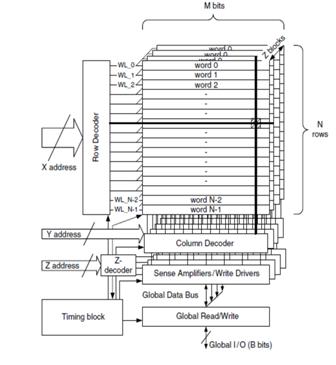
TheessentialelementsofanySRAMusedtostorebinarydata arememorycells.Twocross-coupledinvertersthatcreatea latchandaccesstransistorsmakeupastandardSRAMcell. Accesstransistorsprovideforread-onlyandwrite-onlycell accessaswellascellisolationintheunaccessedstate.Aslong as the cell is powered, an SRAM cell must have nondestructivereadaccess,writecapability,andunlimitedstore (or data retention) duration. Memory cells are organized hierarchically into cores, which may then be further subdivided into blocks and arrays based on the system performance and power needs. A resistive load fourtransistor(4T)SRAMcell,asix-transistor(6T)CMOSSRAM cell, and a load-less 4T SRAM cell are three of the most contemporary SRAM cells. A smaller cell increases the amount of bits per unit area and lowers the cost per bit. Becausetherelatedcapacitancesarelesswithsmallercells, speedandpowerconsumptioncanbeindirectlyimproved.
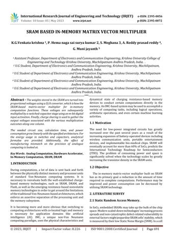
An example of the fundamental SRAM block structure is shownintheabovegraphic.AwordlinefromWL0-WLN-1is chosen bya row decoder that is gated by thetimingblock after decoding the X row address bits. An additional ZdecoderactivatestheaccessedpageinthecaseofanSRAM arraywithNrowsandMbitssetupinapage-likefashion.
Word- or bit-oriented memories are also possible. Each addressinabit-orientedmemorymayaccessasinglebit.
SRAMCell
2.4 Designed by 8T-SRAM as ADOT
Theschematicforatypical8Tbit-cellmaybefoundhere.A decoupledreadportismadeupoftwoextratransistorsin addition to the well-known 6T-SRAM bit-cell. The write word-line (WWL) must be enabled and the write BLs (WBLs/WBLBs)mustbedriventogroundorVDD,depending onthebitthathastobesaved.ThereadBL(RBL)mustbe rechargedtoVDDandthereadWL(RWL)mustbeactivated inordertoreadavaluefromthecell.Keepinmindthatthe source-line(SL)isgrounded
3.
Demandforfastspeed,lowpower,andlownoisesystemsis quitestrong.StaticRandom-Accessmemory(SRAM)canbe utilized for several purposes. The dominant matrix-vector operations,accordingtotheideaofin-memorycomputingfor neuralnetworkapplications,arecarriedoutinthememory itself.TheprecisionofanalogueMACoperationsisaproblem forin-memorycomputing.ByrunningMACoperationsona regularSRAM,theaccuracybarrierisovercome.Theinitial stepinthestrategyistoachievelinearlyscalablecomputing accuracyintermsoftime,power,andarea.
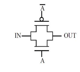
field-effecttransistors,thesubstrateterminal(bulk)isnot internallylinkedtothesourceterminalinFig.3.2.Thedrain and source terminals of the two transistors, an n-channel MOSFET and a p-channel MOSFET, are linked together to formaparallelconnection.ANOTgate(inverter)linkstheir gateterminalstogethertoproducethecontrolterminal.
A transmission gate (TG) is an analogue gate, similar to a relay,thatmaybecontrolledbyacontrolsignalwithnearly anyvoltagepotentialtoconductorblockcurrentineither direction. It is a CMOS-based switch in which PMOS transmits a strong 1 but a poor 0, and NMOS transmits a powerful0butaweak1.BothNMOSandPMOSfunctionat thesametime.Twofield-effecttransistors(FET)makeupa transmission gate, however unlike conventional discrete
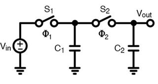
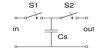
3.2 Switched Capacitor
Aswitchedcapacitor(SC)isanelectricalcircuitthatcarries chargesintoandoutofcapacitorsinresponsetotheopening and closing of electronic switches. The switches are often controlledbynon-overlappingclocksignalssothatnotall switchescloseatonce.Switched-capacitorfiltersarethose thatusethesecomponentsasopposedtoexactresistorsand rely solely on the ratios between capacitances and the switching frequency. As a result, they are far more appropriate for use in integrated circuits than precisely definedresistorsandcapacitors,whicharemoreexpensive tobuild.
SC circuits are generally constructed using the complementary CMOS (CMOS) process and implemented utilising metal oxide semiconductor (MOS) technology, including MOS-capacitors and MOS field-effect transistor (MOSFET) switches. Pulse code modulation (PCM) codecfilters, analogue to digital converter (ADC) chips, mixed signal integrated circuits,andPCM digital telephonyare a fewexamplesofcommonusesforMOSSCcircuits.
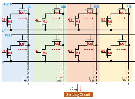
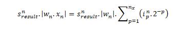
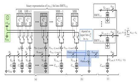
signed IMCU and the related circuit implementation. The recharge voltage selection step and the corresponding circuitry can be skipped in the event of an unsigned multiplication. A multibit fixed-point multiplication of an inputXinbyaweightWncanalsoberestatedasasumofnx binaryproductsifthedistributivelawisapplied.
3.3 Analog Multiplication.
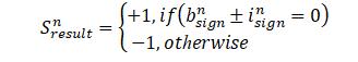
Thevoltagethatisproportionatetotheweightmustthenbe analogly multiplied with the input as the following step. SimilartotheweightWn,itisexpectedthattheinputXnis representedinSMR asa nx-bitfixed-pointnumber.So, by performinganXORoperationbetweentherespectivesigns oftheweight(bnsign)andinput(insign),itispossibleto determinethesignofthemultiplicationresultSnresultright away.
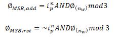
As a result, while processing each bit of the input individually,themultiplicationmaybedoneconsecutivelyin nxmultiplyandaddstages.Thebestwaytoaccomplishthis inhardwareistochangethecontrolsignalsontheswitches oftheMSBcapacitorCnw,whichischargedtoVw,natthe ncyc,w-thcycle.
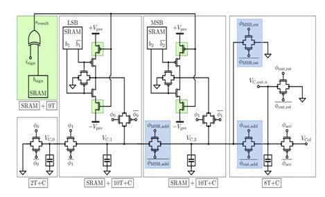
Asaconsequence,theSnresultmaybeusedtodetermine theVprerechargevoltage.Figuredisplaysanexampleofa transistor-level implementation of an SRAM-based 3-bit
Despitehavingmanysimilaritiestooperationalamplifiers, analoguemultipliercircuitsarefarmorepronetonoiseand offset voltage-related issues since these mistakes can compound. Phase-related issues may be very complicated when working with high-frequency transmissions. Widerange general-purpose analogue multipliers are far more difficult to manufacture than operational amplifiers, and theyarefrequentlymadeutilizingspecializedtechnologies andlasertrimming,justashigh-performanceamplifierslike instrumentationamplifiers.Sincetheyarequiteexpensive, they are often only employed in circuits where they are absolutelynecessary.
4. SOFTWARE REQUIREMENTS
A set of tools for designing integrated circuits is called TannerEDA.Withthesetools,youmayenterschematics,run SPICE simulations, create physical designs (such chip layouts), verify design rules (DRC), and do layout versus schematic(LVS)comparisons.

4.1
Threedifferenttoolsare
S-edit
T-SPICEL-edit
Aschematiccapturetools
theSPICEsimulationengineintegratedwithSedit-thephysicaldesigntool
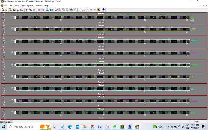
TheSRAM'swaveformsareseenintheabovegraphic.When wedivideawaveintoitsmanyparameters.
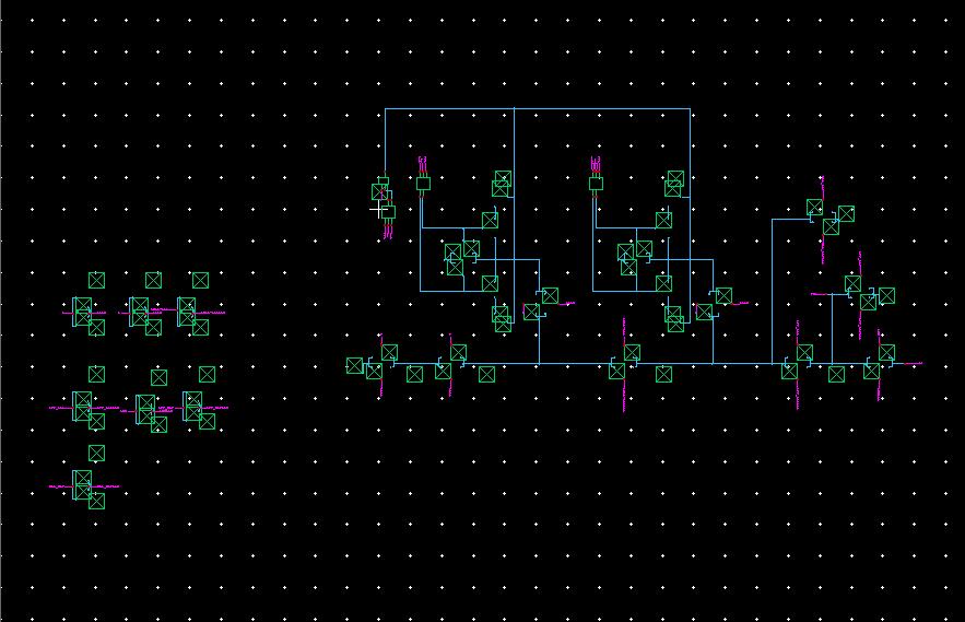
Theschematicperspectiveisdepictedintheabovediagram. TheyhaverevealedAnSram'sinternalrelationshipsaswell asitsstructuraldetails.
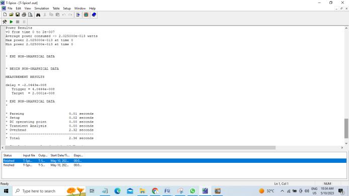
Theeffectofweightandinputquantizationonthemaximum power,averagepower,andmultiplyoperationtime.Dueto the fact that every extra weight bit requires a new set of capacitors, switches, and clock cycles, delay and power consumption both rise linearly. As a result, their product, whichisenergyconsumption,exhibitsasquaredependency. Nevertheless, for the input bits nx, the scaling vs energy stays perfectly linear since pipelining simply necessitates three more cycles of operation for the circuit, with no additionalhardwareneededinsidetheIMCU.
3. CONCLUSIONS
The idea of in-memory computing for neural network applications has been motivated by the time and energy costsinvolvedwithdatatransportation.Thismethodmakes use of specific physical characteristics of memory technologies to conduct the dominant matrix-vector operationsin-place,orinthememoryitself.Ourmethodis thefirsttoachievecomputingaccuracythatgrowslinearlyin time,power,andarea,despitethefactthatthereareseveral SRAM-based matrix-vector multiplication engines in the literature.
The precision of the analogue MAC operations is the fundamentalobstacletoin-memorycomputing.Theareaand power needed can be decreased by switching to 14 nm technologyfrom45nmtechnology.
The SRAM-based multibit in-memory matrix vector multiplier(IMMVM),whichhasthepotentialtodramatically increase the speed and power efficiency of a variety of computing workloads, is a promising technology. Matrixvector multiplication (MVM) may be carried out by the IMMVMarchitecturedirectlyinthememoryarray,obviating the requirement to transfer data back and forth between memoryandtheprocessingunit.Thiscanincreaseoverall systemeffectivenessandlessenthedataflowbottleneck.
REFERENCES
[1] 1.B. Keeth and R. J. Baker, DRAM Circuit Design: A Tutorial,1sted.Hoboken,9NJ, USA:Wiley,2000.
[2] P. F. Ferguson, X. Haurie, and G. C. Temes, “A highly linear low-power 10-bit DAC for GSM,” in Proc. IEEE CustomInteger.CircuitsConf.,May2000,pp.261–264.
[3] M. Le Gallo et al., “Mixed-precision in-memory computing,”NatureElectron.,vol.1,no.4,pp.246–253, Apr.2018.
[4] W. C. Jeong et al., “True 7 nm platform technology featuring smallest FinFET and smallest SRAM cell by EUV, special constructs and 3rdgeneration single diffusionbreak,”inProc.IEEESymp.VLSITechnol.,Jun. 2018.
BIOGRAPHIES
K.G.VENKATA KRISHNA, Assistant Professor, Krishna University College of Engineering and Technology Krishna University, Machilipatnam.
PARASA HEMA NAGA SAI SURYA KUMAR,Student ofDepartmentof Electronics and Communication Engineering, Krishna University, Machilipatnam.

SARIKOKKUMEGHANA,Student ofDepartmentofElectronicsand CommunicationEngineering, KrishnaUniversity, Machilipatnam.

ATURI REDDYPRASADREDDY, StudentofDepartmentof ElectronicsandCommunication Engineering,KrishnaUniversity, Machilipatnam

GODUGUCHINTHAMUNI JAYANTH,Studentof Department ofElectronicsandCommunication Engineering,KrishnaUniversity, Machilipatnam.