International Research Journal of Engineering and Technology (IRJET)

Volume: 09 Issue: 04 | Apr 2022 www.irjet.net
e ISSN: 2395 0056
p ISSN: 2395 0072

International Research Journal of Engineering and Technology (IRJET)
Volume: 09 Issue: 04 | Apr 2022 www.irjet.net
e ISSN: 2395 0056
p ISSN: 2395 0072
1Research Scholar, Department of Electronics & Communication Engg P.K University, Shivpuri M.P, India
2 H.O.D Electronics & Communication Engg. Deptt, P.KUniversity, Shivpuri M.P, India
***
Abstract The performance analysis ofatwo stage CMOS operational transconductance amplifier in conventional gate driven mode is presented in this paper. Theoretical computations as well as computer aided simulation analyses have been detailed. The designs were created using the TSMC 180nm CMOS process. 'Pyxis Schematic' was used for schematic simulations, while the simulator 'Eldo', version 11.2 of Mentor Graphics, was used for simulations. To begin,a DC analysis is used to determine all of the transistors' operating regions. All of the transistors are properly operating in the saturation zone, according to the results. Further AC research reveals that the Op Amp has a gain of 75 dB, a phase margin of 53.8, and aunity gain bandwidth of 30.5MHz. In addition, the input referred noise voltage is 0.0fV/Hz and the CMMR is 77.8dB. The slew rate is 0.37V/s, and the settling time is 472ns, according to transient analysis. Under 1.8V supply voltage, the output swings up to 1.25V, and the op-amp consumes536.5W ofpower.Thesupplyvoltage is scaled to 1.5V and then to 1.2V to achieve a low power op amp. With supply voltage scaling, large power savings of 18% and 35% can be achieved without compromising phase margin and slew rate, and only minor compromises in a few parameters like gain, UGB, and CMRR.
Key Words: (Analog circuit; Low voltage low power; Two stage CMOS operational amplifier; Gain; Phase margin).
Throughoutthecourseofrecentyears,therehasbeen giganticinvestigationsinVLSIventuresbecauseofscaling patterns towards profound submicron innovation. Requests for low power and productive convenient suppliesareascendingineverydaylife.Decreaseofsupply voltage is normal pattern for examining low power circuits. However, in the event of metal oxide semiconductor (MOS) semiconductor, supply voltage shouldbebasicallyequivalenttoormoreprominentthan the limit of MOS semiconductors utilized in circuit acknowledgment. This gives impediments in bringing down of voltage supply after specific cutoff. The quick scalingofCMOSprocessesinnanometerrequestlowstock
which helped advanced circuit acknowledgment at extremelylowpowerutilizationhoweveritisn'tvalidfor simplecircuitacknowledgment.Therelateddownsideis short direct impact which brings about low addition stages,diminishedimpedanceandsoforth.
Functional enhancers are essential components in numeroussimplehandlingframeworks.Everyoneofthe continuoussignsaresimpleinnatureandthusregardless of whether they are handled in computerized space for adaptability and simplicity of handling, functional intensifiersbecomeavitalcomponentinnumeroussimple andinconsistentmessageframeworks Astheinterestfor blended mode coordinated circuits increments for low voltagelowpoweractivity,theplanofsimplecircuitslike functional intensifiers (operation amps) in CMOS innovationturnsouttobemorebasic[1].
Thisstudytargetsexaminingandaddressingdifferent tradeoffs connected with execution examination of ordinary two phase CMOS operation amp at profound submicroninnovationhub.InsegmentII,blockgraphand essentials of two phase CMOS operation amp are talked about. Segment III depicts geography utilized and it's functioning guideline. Plan contemplations are given in SectionIV.Likewisetheparticularsareexplainedandthe recipe and computations for plan of two phase CMOS operation amp are momentarily expounded. Segment V presents the recreation results for different execution boundaries and its relative investigation on execution boundariesfortraditionalentrywaydrivenoperationamp fordifferent stock voltages and afew closing comments showupinSectionVI.
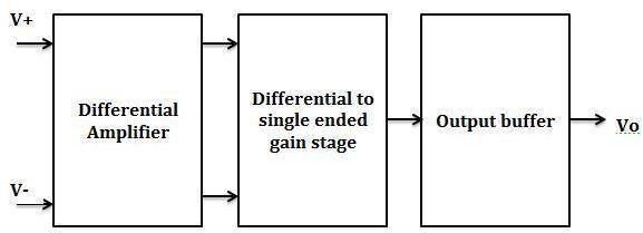
Fig.1 shows essential square graph of an operation amp. It comprises of fundamentally three phases. As displayed in figure 1, the information phase of the operationampcomprisesofadifferentialenhancerandit gives the differential to single finished transformation. Regularly, a the greater part of the piece of the general additionisgivenbythedifferentialinformationstageand thesubsequentstageisordinarilyaninverterornormal sourceamplifier[2].
© 2022, IRJET | Impact Factor value: 7.529 | ISO 9001:2008
Page4028
International Research Journal of Engineering and Technology (IRJET)
Volume: 09 Issue: 04 | Apr 2022 www.irjet.net
Differentialenhancergivesgaininaperfectworldupto 40dB, further necessity of gain is achieved in the subsequentstage.Iftheoperationampshoulddrivealow obstructionload,thesubsequentstageshouldbetrailed byasupportstagewhosegoalistobringdowntheresult opposition and keep an enormous sign swing [18]. The result cushion may some of the time be overlooked to frame a high result opposition un supported operation amp frequently alluded to as Operational Trans conductanceAmplifieroranOTA.Thosewhichhavethe lastresultsupportstagehavealowresultobstructionand arecalledasOperationalAmplifiersorbasicallyOp Amp [17].
To lay out the appropriate working point for every semiconductorinitsquietstate,predispositioncircuitsare given[2].Payisadditionallyremotelygiventoguarantee soundnesswithoutwhichoperationampmightactasan oscillator.Idealoperationamphasboundlessdifferential voltage gain, endless information obstruction and zero result opposition. As a general rule operation amp just methodologiesthesequalities.
CMOSOperationalAmplifierisoneofthemostflexibleand significant structure blocks in simple circuit plan. The essentialnecessityofanoperationampistohaveanopen circle gain that is adequately enormous to carry out regrettable input idea. The result voltage Vout can be communicatedas:
Vout=AV x(V1 V2) (1)
where, AV is used to designate the open loop differential voltagegain.V1andV2aretheinputvoltages applied to the non inverting and inverting terminals, respectively[2]
•Opencirclegain:
The proportion of progress in yield voltage to the adjustmentofvoltageacrosstheinformationterminalsis known as open circle gain of the operation amp. It is otherwisecalleddifferentialmodevoltageintensification.
•Wellknownmodegain:
e ISSN: 2395 0056
p ISSN: 2395 0072
Theproportionofresultvoltagetotheinfovoltagewhen both the terminals of the operation amp are provided same potential is known as familiar mode gain of operationamp.Itisotherwisecalledwellknownmode voltageintensification.
•Wellknownmodedismissalproportion:
The proportion of differential voltage gain to familiar mode voltage gain is known as well known mode dismissal proportion (CMRR). In a perfect world this proportion would be boundless with familiar mode voltagesbeingcompletelydismissed.
•Slewrate:
Therateatwhichtheresultchangesconcerningthetime expectedforastagechangeintheinfoisknownasslew pace of the operation amp. It is for the most part communicatedintheunitsofV/μsec.
•Inputfamiliarmodevoltagerange:
Thescopeoffamiliarmodeinputvoltagethatmightmake the functional enhancer stop working appropriately assumingtheinfovoltagegoespastthisreachisknown asinformationfamiliarmodevoltagerange.
•Solidaritygaintransferspeed:
Thescopeoffrequencies,insidewhichtheopen circleg is more noteworthy that solidarity, is alluded as the solidaritygaindatatransmissionoftheoperationamp.
•Alloutpowerdissemination:
Thecompletedcpowerprovidedtothegadgetlessany powerconveyedfromthegadgettoaheapisknownas absolute power dispersal of the operation amp. At no heap
=VDD
(2)
Theprimaryviewpointconsideredintheplanwasto choosethespecifications(specs)tobemet.Inviewof an unmistakable comprehension of the specs, the circuitgeographyofthestandardCMOSoperationamp waspicked.
© 2022, IRJET | Impact Factor value: 7.529 | ISO 9001:2008
Journal
Page4029
International
Volume: 09 Issue: 04
Journal of Engineering and Technology (IRJET)
Apr
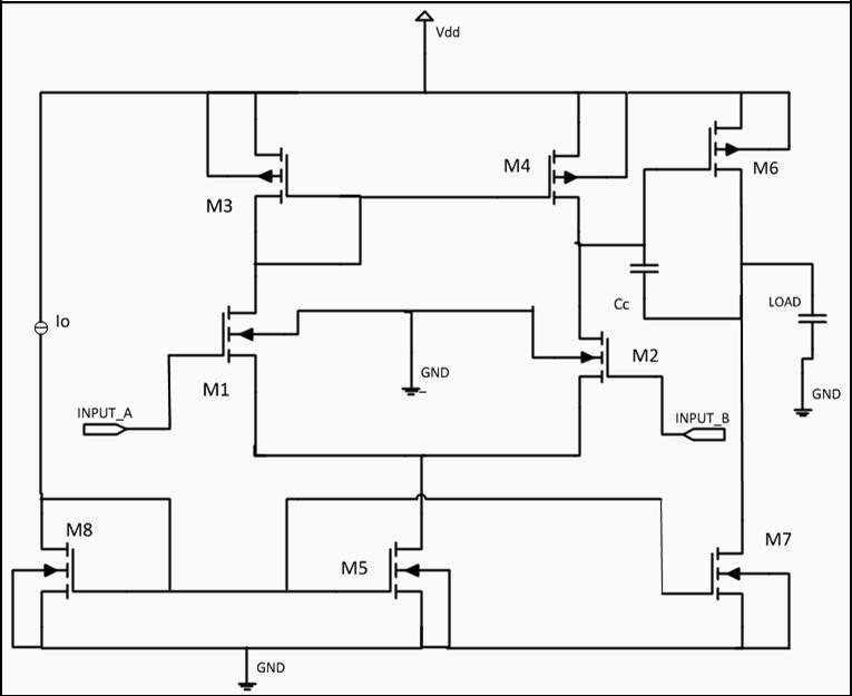
As displayed in fig.2, it is two phase unbuffered door drivenfunctionaltransconductancespeakerwhereinfois appliedfromthetraditionalentrywayterminalofNMOS semiconductors M1 and M2. Alongside M1 and M2, M3 and M4 going about as current mirror load, shapes first phaseofthefunctionalintensifier.M6andM7addressthe subsequentincreasephaseofspeaker.M5andM8involve biasing circuit and Cc addresses the remunerating capacitance.Thistwophaseoperationamp,OTAdisplayed in fig. 2 is generally utilized in view of its design and strength.
Anidealoperationamphavingasolitaryfinishedyieldis described by a differential info, boundless voltage gain, limitless information opposition and zero result obstruction[18].Inactualityoperationampanywaythese qualitiescan'tbeproducedhowevertheirexhibitionmust be adequately really great for the circuit conduct to intentlyroughthecharactersofanidealoperationampin manyapplications.Withthepresentationofeachnewage of CMOS innovations plan of operation amps keeps on actingfurtherdifficultieslikethestock
voltages and semiconductor channel lengths downsize. Subsequentlyinthisworkfundamentalpointistoplanthe OTA in 180nm innovation and to do the presentation examinationofdifferentattributes.
Fortheplanofsimplecircuits,havingdeterminationsfor itscustomizationisobligatory.Particularsareseparated intotwoclasses.Firstiscircuitparticularwhichisgivenby the creator or producer for its plan, and second is EDA apparatus detail which is given by the EDA device merchant.
SupplyVoltage,VDD=1.8V
e ISSN: 2395 0056
p ISSN: 2395 0072
Openloopgain,AV=1000=60dB
PhaseMargin=600
LoadCapacitance,CL=2pf
MaximumInputCommonModeRange,ICMR(+) =1.8V
MinimumInputCommonModeRange,ICMR( )= 0.9V
Slewrate=20V/μsec
PowerDissipation<0.3mW
GainBandwidthProduct,GBW=30MHz
μnCox=221.55μA/V2
Vthn=0.37V
μpCox=93.87μA/V2
Vthp= 0.39V
Designing has been conceived on the basis of fundamentalequationswhichareusedforthecalculations ofaspectratios.TheDCgainofthefirststageis
TheDCgainofsecondstageis
OverallgainoftheOp amp
SlewrateofconventionalOp ampis
WhereI5isthecurrentthroughtheM5transistorandit isthebiascurrentoftheinputstage
TheGainbandwidthoftheOp ampis
International Research Journal of Engineering and Technology (IRJET)
Volume: 09 Issue: 04 | Apr 2022 www.irjet.net
PowerdissipationofOp ampisgivenby (9)
Following table I shows simulation parameters includingcalculated valuesofthe aspectratiosobtained fromthetheoreticalperformanceanalysisofop ampusing above equations from circuit technology & also the fundamentalequationsfromtheCMOStechnology
VDD 1.8V
Powerconsumption 373.5µW
Inputbiasrange 20µA (W/L)1,(W/L)2 6 (W/L)3,(W/L)4 4 (W/L)5,(W/L)8 20 (W/L)6 75 (W/L)7 175
The circuit was reenacted utilizing Eldo with BSIM3v3.3 level 53 model in view of a TSMC 180 nm CMOS process. The OP AMP works with the 1.8V power supply and consumes just 536.5μW power. Recreations results for DC, AC and transient examination are made senseofinthissegmentfordifferentelectricalqualities.
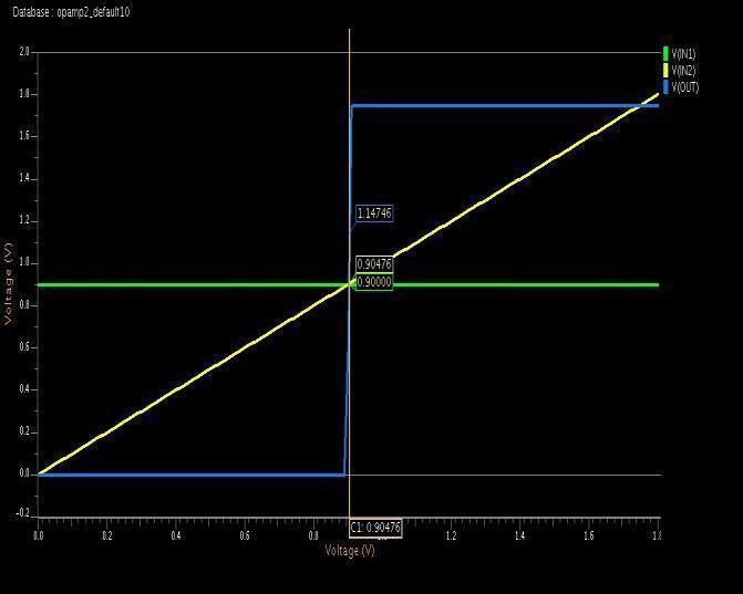
InDCexamination,districtofactivityofnotentirelysetin stone. Here in two phase functional transconductance enhancer, every semiconductor should be in immersion district.DuringDCinvestigation,allACapplicablepartsfor examplecapacitor,inductorandsoonaresettonothing. This examination is significant for delivering attributes movebendasdisplayedinfig.3
© 2022,
e ISSN: 2395 0056
p ISSN: 2395 0072
Fig3:DCanalysisofop amp
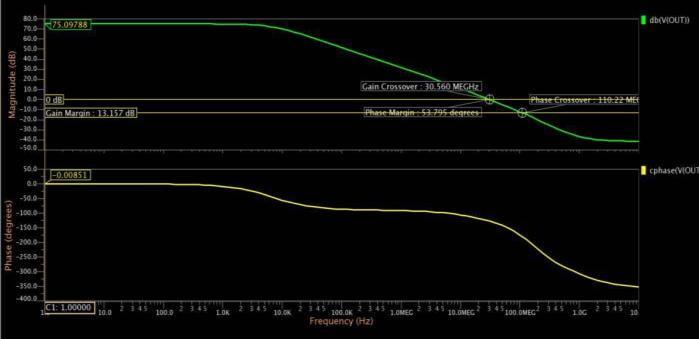
InACanalysiswedeterminePhase margin,Gainand unity gain bandwidth of the operational amplifier. Both GainandPhasemarginarecalculatedusingDCoperating pointandACanalysis.Thefrequenciesusedtoimplement AC analysisare
• StartFrequency=1Hz
• StopFrequency=1GHz
Impact Factor value: 7.529
Fig4:ACanalysisofop amp
Duringtransientanalysis,firstaninitialoperatingpointis calculated(basedonDCvalues)andafterthatallmomentary voltagesandcurrentarecomputedastheresultsofatime dependent well behaved input voltage or current source includingtheinfluenceofcapacitors.
Volume:
TheOp AmphasbeenplannedinaTSMC180nminnovation with1.8Vsingleinventory.Reproductionshavebeenfinished utilizing Eldo with a BSIM3v3.3 level 53 semiconductor modelfortheTSMC180nmCMOSinnovation.Atfirstithas beenguaranteedthateveryoneofthesemiconductorsare workingimmersionthroughDCOPandDCinvestigationas displayedinfig.3
Thestageedgeandtheopen circlegainoftheOp Ampwitha heap capacitance CL =1 pF are portrayed in fig4. The DC open circlegainis75.1dB,withastageedgeof53.8ºdegrees whiletherecreatedsolidaritygainrecurrenceis
30.56MHzasdisplayedinfig4.
The transient examination displayed in fig. 5 additionally demonstratestheassessedabundancyoftheincreasegotin ACexamination.Thepowerdisseminationofthemimicked functionalintensifieris536.5μW.
Slew rate (SR) has been gotten by reenactment in a non altering voltage supporter arrangement. With a capacitive heapof5pFassociatedwiththespeakeryields,thedeliberate slew raterisesto0.37V/μs.Fig.6showsthereactionofthe frameworkfora0.8Vadvanceinformationsignals.3
Thisresearchexaminestheperformanceofatwo stage OTA built in TSMC 180 nm technology. The developedOp ampmeetsnearlyallparameters,including ahighDCgainof75.1dB,UGBof30.5MHz,PhaseMargin of53.8,andCMRRof77.7dB,accordingtotheresults.With aloadcapacitanceof5pFandasettlingperiodof270ns, thetwo stageCMOSop ampslewsat0.37V/s.Italsohasa 1.75Voutputswingwitha2pFloadanda1.05VICMR.For the supply voltage of 1.8V, simulations show a power dissipation of 536.5W The supply voltage scaling approach reduces it even more. The results reveal that significant power savings can be accomplished, with savingsof18%and35%forsupplyvoltagescalingof1.5V and 1.2V, respectively. It can also be obtained with
e
p
2395
minimalcompromisesinphasemarginandslewrate,as well as a few other properties such as gain, UGB, and CMRR. Even yet, by operating transistors in the subthresholdregionoremployingbulkdriventransistors, powerdissipationcanbefurtherlowered.
[1] Khateb,Fabian,Biolek,Dalibor,Khatib,Nabhamand Vavra,Jiri(2010),“UtilizingtheBulk drivenTechniquein Analog Circuit Design”, 978 1 4244 6613 9/10@2010 IEEE.
[2] Allen,P.E.andHolberg,D.R.(2002),LCMOSAnalog CircuitDesign,NewYork:OxfordUniv.Press2002.
[3] Mancini, Ron, OPAmps for Everyone, Texas Instruments,August2002,11.1 11.22.
[4]Kargaran,E.,Khosrowjerdi,H.andGhaffarzadegan,K. (2010),“A1.5vHighSwingUltra Low PowerTwoStage CMOS OP AMP in 0.18 μm Technology”, in Mechanical and Electronics Engineering (ICMEE), 2010 2nd International Conference, Vol. 1, pp. V1 68 V1 71, 1 3 Aug.2010,doi:10.1109/ICMEE.2010.5558594
[5] Kar, Sougata Kumar and Sen, Siddharta (2012), “A HighlyLinear CMOSTransconductanceAmplifierin180 nmProcessTechnology”,AnalogIntegrCircSigProcess, Vol.72,pp.163 171,Springer.
[7]Luca, M., Francesco,A.A., Felice, C., Gregorio, C. and Giuseppe,(2012),“Designofa75 nW,0.5VSubthreshold ComplementaryMetal oxidesemiconductorOperational Amplifier”, International Journal of Circuit Theory & Applications,2012.
[8]Gupta,A.,Mishra,D.K.,Khatri,R.,Chandrawat,U.B.S. andJain,P.(2010),“ATwoStageandThreeStageCMOS OPAMPwithFastSettling,HighDCGainandLowPower Designed in 180nm Technology,” in Computer Information Systems and Industrial Management Applications(CISIM),2010InternationalConferenceon, pp. 448 453, 8 10 Oct. 2010 doi: 10.1109/CISIM.2010.5643497
[9]Zhang,J.Y.etal.(2009),“DesignofLow offsetLow power CMOSAmplifier for Biosensor Application”, J. of BiomedicalScienceandEngineering,Vol.2,pp.538 542.