International Research Journal of Engineering and Technology (IRJET)
e-ISSN: 2395-0056
Volume: 05 Issue: 06 | June 2018
p-ISSN: 2395-0072
www.irjet.net
Design of Capacitor less LDO Regulator by using cascode compensation technique Vartul Sharma1, Vanita Agarwal2
1M.Tech,
Electronics and Telecommunication Department, College of Engineering, Pune, India Professor, Electronics and Telecommunication Department, College of Engineering, Pune, India ---------------------------------------------------------------------***--------------------------------------------------------------------2Assistant
Abstract - This paper discusses two different
means a low output resistance (and thus low load regulation) can be achieved by high DC loop gain. Low dropout and low quiescent current (Iq) are required for low power dissipation thus increasing the efficiency of the LDO regulator [1-2]. In short, a good LDO regulator should have high dc loop gain, low load and line regulations, wide bandwidth and low quiescent current. While the circuit requirements are quite obvious, it is difficult to achieve all of them due to a lot of trade-offs between these parameters. The detailed discussion is in subsequent sections. Section 2 discusses about the basic LDO circuit operation and its main drawback with a basic design example. In section 3, a capacitor less approach of designing LDO regulators is discussed in detail. A capacitor less LDO design using cascode compensation technique is also discussed and presented here with results. Section 4 compares the two design styles to conclude.
methodologies to design a Low Dropout Voltage Regulator (LDOVR) with their applications. In the first approach, a basic LDO regulator is designed which uses a compensation capacitor to achieve stability. The dropout voltage of this LDO is 200mV with an output voltage of 1.4V. For worst case stability, bandwidth and phase margin (PM) are 475.67 KHz and 43.85 degrees. Another LDO is also designed with capacitor less approach having high DC loop gain and wide bandwidth. This design having a dropout voltage of 100 mV uses a miller compensation capacitor to achieve stability along with a series resistor to shift the right half plane zero to left half plane which leads to high bandwidth. A total of 80pF capacitor and 50 Kohms resistance are used to achieve proper stability with bandwidth of 2.55 MHz and PM of 63 degrees in worst case stability scenario. Key Words: LDO Regulator, cascode compensation, Ahuja compensation, capacitor less LDO, LDOVR
2. BASIC LDO REGULATOR
1. INTRODUCTION
2.1 Circuit operation:
The Voltage Regulator is a key part of power management circuitry in integrated circuits. Voltage regulators are used to supply a constant voltage in spite of variations in load and power supply. With the reduction in supply voltage and demand of low power designs, LDO regulators are becoming an obvious choice for design engineers. The market need for portable devices is truly driving the technology of LDO regulators. The most fundamental requirement of an LDO regulator is a constant output voltage irrespective of supply and load variations. While this is easily achieved for various load currents and supply voltages, the problem arises when there is a sudden change in the line voltage or load current. The output voltage may go through some overshoots and undershoots before settling down to the previous voltage. This is due to the fact that the loop takes some time to regulate. To reduce the loop regulation time, we want high bandwidth. High phase margin is required to reduce the ringing of output voltage during transients. Another very important requirement of the LDO regulator is low load and line regulations. While line regulation is a measure of change in output voltage with respect to change in supply voltage (V/V), load regulation depicts the change in output voltage with load current variations (V/I), which is nothing but output resistance of the circuit. An LDO uses a shunt feedback for the regulation which Š 2018, IRJET
|
Impact Factor value: 7.211
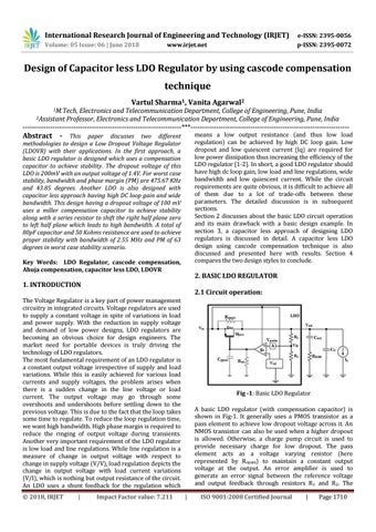
Fig -1: Basic LDO Regulator A basic LDO regulator (with compensation capacitor) is shown in Fig-1. It generally uses a PMOS transistor as a pass element to achieve low dropout voltage across it. An NMOS transistor can also be used when a higher dropout is allowed. Otherwise, a charge pump circuit is used to provide necessary charge for low dropout. The pass element acts as a voltage varying resistor (here represented by Ropass) to maintain a constant output voltage at the output. An error amplifier is used to generate an error signal between the reference voltage and output feedback through resistors R1 and R2. The |
ISO 9001:2008 Certified Journal
|
Page 1710