
Mouser Electronics:
years of innovation and the future of continued growth May/June 2024 Vol.43 No.6 PP100007394
60


In 2024, Mouser Electronics celebrates its 60th year in business, a testament to its enduring success. The company’s longevity can be attributed to its commitment to innovation, customer service and adaptability in the ever-evolving electronics industry. As the worldwide market for semiconductors and electronic components continues to grow, Mouser remains poised to capitalise on these opportunities through strategic business development plans.
Looking ahead to 2024, Mouser sees significant growth opportunities in emerging technologies such as Internet of Things (IoT), artificial intelligence and renewable energy. The company is also focusing on expanding its presence in Australia and New Zealand, leveraging their evolving markets and fostering partnerships with local industries.
Mouser’s dedication to staying ahead of industry trends has led to involvement in groundbreaking projects, showcasing their expertise and capabilities. Moving forward, Mouser aims to achieve goals centred on continued innovation, customer satisfaction and sustainable growth, solidifying its position as a leading distributor of electronic components worldwide.
WWW.ELECTRONICSONLINE.NET.AU MAY/JUN 2024 3 CONTENTS 4 Advanced microchips developed for modern AI workloads 15 Australia's largest electronics expo returns to Sydney 22 Tuneable coloured films for displays and sensors 32 Brain-inspired system gathers data from salt-sized sensors 39 Compact chips could enhance navigation and communication 42 Recyclable circuit board turns to jelly for disassembly 45 Hidden semiconductor activity spotted by researchers 50 Wearable sensor measures real skin feel Your copy of What's New in Electronics is available as an online eMag. READ ONLINE! www.electronicsonline.net.au/magazine
Electronics au.mouser.com COVER
Mouser
STORY
May/June 2024 Vol.43 No.6 PP100007394
Mouser Electronics: 60 years of innovation and the future of continued growth

ADVANCED MICROCHIPS DEVELOPED FOR MODERN AI WORKLOADS
4 MAY/JUNE 2024 WWW.ELECTRONICSONLINE.NET.AU
iStock.com/da-kuk

The US Defense Department’s Defense Advanced Research Projects Agency (DARPA) has partnered with Princeton University to develop advanced microchips for artificial intelligence.
The new hardware reimagines AI chips for modern workloads and can run powerful AI systems using less energy than current advanced semiconductors, according to Naveen Verma, Professor of Electrical and Computer Engineering. Verma, who will lead the project, said the advance breaks through the barriers that have stymied chips for AI, such as size, efficiency and scalability.
Chips that require less energy can be deployed to run AI in more dynamic environments, from laptops and phones to hospitals and highways to low-Earth orbit and beyond. DARPA will support Verma’s work, based on a suite of key inventions from his lab, with an $18.6 million grant. The DARPA funding will drive an exploration into how fast, compact and power-efficient the new chip can get.
“There’s a pretty important limitation with the best AI available just being in the data centre. You unlock it from that and the ways in which we can get value from AI, I think, explode,” Verma said.
In the Princeton-led project, researchers will collaborate with Verma’s startup, EnCharge AI. The startup aims to commercialise technologies based on discoveries made from Verma’s lab, including several key papers he co-wrote with electrical engineering graduate students going back to 2016. Verma cofounded EnCharge AI in 2022 with Kailash Gopalakrishnan, a former IBM Fellow, and Echere Iroaga, a leader in semiconductor systems design.
Gopalakrishnan said that innovation within existing computing technologies, as well as improvements in silicon technology, began slowing at the time when AI began creating new demands for computation power and efficiency. Not even the best graphics processing unit (GPU), used to run today’s AI systems, can mitigate the bottlenecks in memory and computing energy facing the industry. “While GPUs are the best available tool today, we concluded that a new type of chip will be needed to unlock the potential of AI,” Gopalakrishnan said. >
WWW.ELECTRONICSONLINE.NET.AU MAY/JUN 2024 5
ARTIFICIAL INTELLIGENCE
To meet the rising demand for computing power required by AI models, the latest chips pack in tens of billions of transistors, each separated by the width of a small virus. And yet the chips still are not dense enough in their computing power for modern needs.
Today’s leading models, which combine large language models with computer vision and other approaches to machine learning, were developed using more than a trillion variables each. The Nvidia-designed GPUs that have fuelled the GPU boom have become so valuable, there is reportedly a considerable backlog to buy or lease these chips.
To create chips that can handle modern AI workloads in compact or energy-constrained environments, the researchers had to reimagine the physics of computing while designing and packaging hardware that can be manufactured with existing fabrication techniques and that can work well with existing computing technologies, such as a central processing unit. “AI models have exploded in their size and that means two things. AI chips need to become much more efficient at doing math and much more efficient at managing and moving data,” Verma said.
The researchers’ approach has three key parts; the core architecture of virtually every
digital computer has followed a deceptively simple pattern first developed in the 1940s: store data in one place, do computation in another. That means shuttling information between memory cells and the processor. Over the past decade, Verma has researched an updated approach where the computation is done directly in memory cells, called inmemory computing. That is part one — the promise is that in-memory computing will reduce the time and energy it costs to move and process large amounts of data. So far, digital approaches to in-memory computing have been limited. As a result, Verma and his team turned to an alternate approach as part two: analog computation.
“In the special case of in-memory computing, you not only need to do compute efficiently, you also need to do it with very high density because now it needs to fit inside these very tiny memory cells,” Verma said.
Rather than encoding information in a series of 0s and 1s and processing that information using traditional logic circuits, analog computers leverage the richer physics of the devices. The curvature of a gear, or the ability of a wire to hold electrical charge. Digital signals began replacing analog signals in the 1940s, primarily because binary code
scaled better with the exponential growth of computing. But digital signals don’t tap deeply into the physics of devices and as a result, they can require more data storage and management. They are also less efficient in that way. Analog gets its efficiency from processing finer signals using the intrinsic physics of the devices, but that can come with a trade-off in precision.
“The key is in finding the right physics for the job in a device that can be controlled exceedingly well and manufactured at scale,” Verma said.
The researchers found a way to carry out highly accurate computation using the analog signal generated by capacitors specially designed to switch on and off with exacting precision. That’s part three. Unlike semiconductor devices such as transistors, the electrical energy moving through capacitors doesn’t depend on variable conditions like temperature and electron mobility in a material.
“They only depend on geometry. They depend on the space between one metal wire and the other metal wire. And geometry is one thing that today’s most advanced semiconductor manufacturing techniques can control extremely well,” Verma said.

WHILE GPUS ARE THE BEST AVAILABLE TOOL TODAY, WE CONCLUDED THAT A NEW TYPE OF CHIP WILL BE NEEDED TO UNLOCK THE POTENTIAL OF AI.
6 MAY/JUNE 2024 WWW.ELECTRONICSONLINE.NET.AU
iStock.com/undefined undefined
ARTIFICIAL INTELLIGENCE
STM32H7R/S
Scalable and secure bootflash microcontrollers

• Arm® Cortex®-M7 running at up to 600 MHz, 1284 DMPIS
• Real-time execution from internal or external memories
• High-speed serial and parallel memory interfaces up to 200 MHz DTR
• Large internal SRAM
• Flexible external memory capacity
• 10 packages: from cost-effective 68 to 225 pins
• Target security certifications: SESIP Level 3 and PSA certified L3
• On-the-fly decrypt/encrypt & secure boot
• Powerful 2.5D NeoChrom GPU - smart DMA architecture memory/GPU
• Enabling UIs with HD resolution
Suite 703, 247 Coward Street, Mascot, 2020, NSW Australia Tel: +61 2 9158 7201 Email: clifford.shi@st.com ARROW Electronics Australia Pty Ltd - Tel +61 2 9737 4900 Future Electronics - Tel: +61 2 8064 0000 Avnet Electronics (Australia) Ltd - Tel: 1300 791 695
NANOTHIN MEMORY CHIPS MANUFACTURED WITH 2D PRINTING
Engineering researchers from the University of Sydney have developed a 2D printing process using liquid metals that could create new ways of creating more advanced and energy-efficient computing hardware that is manufactured at the nanoscale. The development comes amid increasing demand for memory devices, which require significant amounts of energy to produce and use.
Dr Mohammad Ghasemian, the study’s lead author, said reducing the temperature at which zirconium and hafnium become liquid is crucial for developing lower-cost electrical devices, as less energy is required. The researchers first combined tin, zirconium and hafnium in a precise ratio, thus allowing the alloy to be melted below 500°C,
lower than the individual melting points for zirconium (1855°C) and hafnium (2227°C).
The liquid metal alloy has a thin oxide layer while maintaining a liquid centre, and is used to harvest the ultra-thin tin oxide nanosheets doped with hafnium zirconium oxide. “Tin is abundant, low-cost and can be used at a large scale for the manufacture of critical semiconductors, transistors and memory chips. Though hafnium zirconium oxide is a well-known ferroelectric material used in nanoscale applications, like memory devices and sensors, obtaining nanosheets using conventional techniques is both difficult and costly,” Ghasemian said.
The researchers applied the tin-zirconium-hafnium alloy to harvest the nanothin tin oxide layer doped with hafnium zirconium oxide through exfoliation — lifting it from its liquid surface — so it could then be 2D printed on a substrate as ferroelectric nanosheets. These sheets are designed to form the basis of next-generation computing hardware, such as semiconductors and memory chips. Ghasemian likened the alloy to a marble coated in ink.
“The alloy is like a solvent that allows us to remove that ink and then use it for printing. Our process allows us to harvest this precious crust layer and turn it into ultra-thin sheets, which are then used to manufacture electronics. It could be a new source of functional 2D materials which are not accessible by conventional methods. This process allows us to introduce ferroelectricity into much smaller, 2D metal oxides, allowing for the development of next-generation nanoelectronics at low temperatures,” Ghasemian said.
The research findings were published in the journal Small

SCIENTISTS UNVEIL NOVEL MATERIAL FOR MAGNESIUM BATTERIES
Researchers at Tohoku University have developed a novel cathode material for rechargeable magnesium batteries (RMBs) that enables efficient charging and discharging, even at low temperatures. This new material leverages an enhancing rock salt structure and could support the development of energy storage solutions that are safer and higher in capacity.
The study shows a significant improvement in magnesium (Mg) diffusion within a rock salt structure, a notable advancement since the denseness of atoms in this configuration had previously impeded Mg migration. By introducing a mixture of seven different metallic elements, the researchers created a crystal structure abundant in stable cation vacancies, facilitating easier Mg insertion and extraction. The high entropy strategy utilised by the researchers allowed the cation defects to activate the rock salt oxide cathode.
This development also addresses a limitation of RMBs — the difficulty of Mg transport within solid materials. Until now, high temperatures were required to enhance Mg mobility in conventional cathode materials, such as those with a spinel structure. Now, the novel material developed by Tohoku University operates efficiently at 90°C, demonstrating a reduction in the required operating temperature.
Tomoya Kawaguchi, a professor at Tohoku University, said that although lithium is scarce and unevenly distributed, magnesium is abundantly available and offers a more sustainable alternative for lithium-ion batteries. “Magnesium batteries, featuring the newly developed cathode material, are poised to play a pivotal role in various applications, including grid storage, electric vehicles and portable electronic devices, contributing to the global shift towards renewable energy and reduced carbon footprints,” Kawaguchi said.
Tetsu Ichitsubo, a professor at Tohoku University, said that this research harnesses the intrinsic benefits of magnesium, thereby overcoming previous limitations and paving the way for the next generation of batteries. Ultimately the development marks a step forward in the quest for efficient, eco-friendly energy storage solutions.
The research findings have been published in the Journal of Materials Chemistry A
8 MAY/JUNE 2024 WWW.ELECTRONICSONLINE.NET.AU
iStock.com/da-kuk
iStock.com/sefa ozel

RESEARCHERS DEVELOP ENERGYEFFICIENT PROBABILISTIC COMPUTER
Researchers from Tohoku University and the University of California, Santa Barbara have developed a probabilistic computer prototype that combines a complementary metal-oxide semiconductor (CMOS) circuit with a limited number of stochastic magnets, creating a heterogeneous probabilistic computer.
Developing computers capable of efficiently executing probabilistic algorithms frequently used in artificial intelligence and machine learning is a challenge that researchers are seeking to overcome. The approach outlined by researchers in this work represents a feasible solution, with the researchers confirming that the prototype’s enhanced computational performance and energy efficiency surpasses current CMOS technology. The research findings have been published in the journal Nature Communications
Recent artificial intelligence and machine learning have had a transformational impact on society; in such technologies, probabilistic algorithms are utilised to solve problems where uncertainty is inherent or where an exact solution is computationally infeasible. These operations follow specific instructions within CMOS circuits, but sometimes inconsistencies can exist between how software (instructions) and hardware (circuits) work together, leading to discrepancies in outcomes. As the role of artificial intelligence and machine learning expands, there is rising demand for a new computing paradigm that can achieve greater sophistication while reducing energy consumption.
In this study, Professor Shunsuke Fukami from Tohoku University developed a near-future heterogeneous version of a probabilistic computer tailored for executing probabilistic algorithms and facile manufacturing. “Our constructed prototype demonstrated that excellent computational performance can be achieved by driving pseudo random number generators in a deterministic CMOS circuit with physical random numbers generated by a limited number of stochastic nanomagnets. Specifically speaking, a limited number of probabilistic bits (p-bits) with a stochastic magnetic tunnel junction (s-MTJ) should be manufacturable with a near-future integration technology,” Fukami said.
The researchers clarified that the final form of the spintronics probabilistic computer, primarily composed of s-MTJs, will yield a four-order-of-magnitude reduction in this area and a three-order-ofmagnitude reduction in energy consumption compared to current CMOS circuits when running probabilistic algorithms.
Ultimately, the researchers’ prototype addresses the limitations of current deterministic CMOS circuits for artificial intelligence and machine learning. “We anticipate future research and development will advance, leading to the implementation in society of an innovative computing hardware that boasts exceptional computational performance and energy-saving capabilities,” Fukami said.
HYBRID SODIUMION BATTERY CAN BE CHARGED IN A FEW MINUTES

Sodium (Na) has recently garnered attention for its potential in sodium-ion battery technologies. However, existing sodium-ion batteries face fundamental limitations, including lower power output, constrained storage spaces and longer charging times, thereby necessitating the development of next-generation energy storage materials. Researchers from KAIST (Korea Advanced Institute of Science and Technology), led by Professor Jeung Ku Kang, have now developed a high-energy, high-power hybrid sodium-ion battery capable of rapid charging.
The innovative hybrid energy storage system integrates anode materials typically used in batteries with cathodes suitable for supercapacitors. This combination allows the device to achieve high storage capacities and rapid chargedischarge rates, making it a viable next-generation alternative to lithium-ion batteries.
However, the development of a hybrid battery with high energy and high power density requires an improvement to the slow energy storage rate of battery-type anodes as well as the enhancement of the relatively low capacity of supercapacitor-type cathode materials. To account for this, Kang’s team used two distinct metal-organic frameworks for the optimised synthesis of hybrid batteries. This approach led to the development of an anode with improved kinetics through the inclusion of fine active materials in porous carbon derived from metal-organic frameworks. A high-capacity cathode material was also synthesised and the combination of the cathode and anode materials allowed for the development of a sodium-ion storage system that optimised the balance and minimised the disparities in energy storage rates between the electrodes.
The assembled cell, comprising the newly developed anode and cathode, forms a high-performance hybrid sodium-ion energy storage device. This device reportedly surpasses the energy density of commercial Li-ion batteries and exhibits the characteristics of supercapacitors’ power density. It is expected to be suitable for rapid charging applications ranging from electric vehicles to smart electronic devices and aerospace technologies.
Kang said that the hybrid sodium-ion energy storage device represents a breakthrough in overcoming the current limitations of energy storage systems. The research findings have been published in the journal Energy Storage Materials.
news_128945_1_istock-149636960.jpg
10 MAY/JUNE 2024 WWW.ELECTRONICSONLINE.NET.AU
iStock.com/Black_Kira
iStock.com/Andrei Berezovskii
HANDHELD SENSOR ENABLES RAPID DETECTION OF MULTIPLE BACTERIA
Rapid detection of bacteria such as E. coli or salmonella is crucial for preventing outbreaks of foodborne illnesses. Now, researchers from Osaka Metropolitan University have created a handheld device that facilitates quick onsite detection of bacteria. Led by Professor Hiroshi Shiigi from Osaka Metropolitan University, the researchers experimented with a biosensor that can simultaneously detect multiple disease-causing bacterial species within an hour.
“The palm-sized device for detection can be linked to a smartphone app to easily check bacterial contamination levels,” Shiigi said.
The researchers synthesised organic metallic nanohybrids of gold and copper that do not interfere with each other, so that electrochemical signals can be distinguished on the same screen-printed electrode chip of the biosensor. These organic-inorganic hybrids are made up of conductive polymers and metal nanoparticles. The antibody for the specific target bacteria was then introduced into these nanohybrids to serve as electrochemical labels.
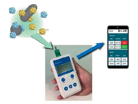
From left: Image of bacteria labelled with electrochemical markers, an electrochemical instrument to measure the data, and an image of the data displayed on a smartphone.
Results confirmed that the synthesised nanohybrids functioned as efficient electrochemical labels, enabling the simultaneous detection and quantification of multiple bacteria in less than an hour.
“This technique enables rapid determination of the presence or absence of harmful bacteria prior to shipment of food and pharmaceutical products, thereby helping to quickly ensure safety at the manufacturing site,” Shiigi said.
The researchers now aim to develop new organic metallic nanohybrids to detect even more bacterial species. The research findings were published in the journal Analytical Chemistry


WWW.ELECTRONICSONLINE.NET.AU MAY/JUN 2024 11
Hiroshi Shiigi, Osaka Metropolitan University.
COMPACT EDGE SYSTEM
The Advantech EI-53 Compact Edge System is powered by 13th Gen Intel Core Mobile processors with up to 10 cores and DDR5 5200 MHz dual-channel memory up to a maximum capacity of 64 GB. It also features Intel Iris Xe integrated graphics. The device’s computing capability is designed to integrate with pre-installed software tailored for industrial applications. It features the Advantech SUSI API for GPIO, CANBUS access, DeviceOn for OTA updates, remote monitoring, real-time management and ready with Ubuntu 22.04. Additionally, a robotics software package expedites robotics applications, complemented by a pre-built Robotics SDK. With its extensive I/O connectivity and integrated software packages, the device caters to semiconductor equipment, robotics & AMR, and energy storage applications, supporting industry standard protocols. It also received the IoT Edge Computing Excellence Award from IoT Evolution World.
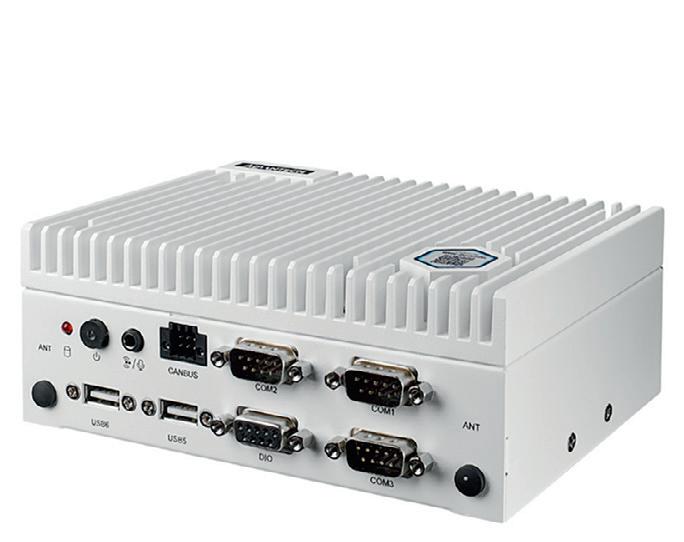
The compact edge system is equipped with a range of I/O ports including 2 x CANBus, 3 x RS-232/422/485, 2 x LAN (with one up to 2.5 G), 6 x USB and DI/O. It utilises its space to accommodate an M.2 M-key 2280/E-Key 2230/B-key 3042&3052, allowing for advanced LTE, 5G, Wi-Fi and AI module connectivity. In terms of display interfaces, the device supports dual 4K lockable HDMI 2.0b, with ultra-high 4096 x 2160 resolution. These I/O options meet the demand for various types of connectivity.
The device is designed to facilitate remote management with its integrated Advantech DeviceOn software. This software streamlines centralised management, data integration, real-time monitoring and OTA updates for both software and firmware batches. Furthermore, the SUSI API acts as a bridge, simplifying and enhancing the synergy between hardware and software. It provides system protection, device monitoring, I/O control and application extension on Advantech platforms.
The system comes preconfigured with a Robotics SDK, easing the development process for robotics applications. It supports toolkits such as Rviz, Movelt and NAV2 on Linux. Finally, as an Ubuntu Ready System, it provides security updates, tri-weekly CVE maintenance and five years of long-term support (LTS). These features collectively make the Advantech EI-53 suitable for robotics and AMR applications. Advantech Australia Pty Ltd www.advantech.net.au
SMART DEVICE INPUT CONNECTOR
MONITORING RECEIVER
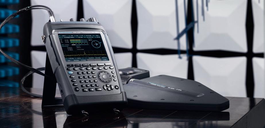
The R&S PR200 is a versatile monitoring receiver for field operations with a 40 MHz real-time bandwidth over a wide frequency range of 8 kHz to 8 GHz — extensible to 20 GHz or 33 GHz with the R&S HE400DC or R&S HE800-DC30 handheld antennas, both with integrated downconverters. The monitoring receiver features a wide range of measurement functions and comprehensive signal analysis capabilities, making it suitable for complex signal measurements including 5G signals.
The portable receiver is designed for use in demanding field operations, with minimal size, weight and power consumption (SWaP) combined with enhanced RF performance and usability. The receiver can handle typical tasks in every mobile spectrum monitoring, spectrum clearance, interference hunting and site testing mission, both for indoor and outdoor environments.
The R&S PR200 is suitable for regulatory authorities, mobile network operators, police forces, military units and other security organisations. They can use the portable receiver to search for and analyse known and unknown radio emissions and to localise signal sources. Rohde & Schwarz (Australia) Pty Ltd www.rohde-schwarz.com.au
The SCHURTER Smart Connector DS11 PEM is a smart device input connector with WLAN connectivity. By installing the Smart Connector and using the SCHURTER Smart Ecosystem, users can have all the functions necessary for an IoT-enabled device.
By recording values such as power consumption, performance and voltage, usage patterns can be identified and device operation optimised. In addition, information can be exchanged via an API interface.
The SCHURTER Smart Ecosystem consists of the Smart Connector, the SCHURTER Cloud, the Smart Dashboard, the Smart App for Apple and Android, and the Smart API. The dashboard and the app offer convenient access to the device data at any time.
The Smart Dashboard is the browser-based, visual interface to the SCHURTER Cloud. Devices equipped with a Smart Connector can be controlled, monitored and managed in the dashboard. In addition, the Smart Dashboard is a flexible platform. If required, individual functions can be programmed or the Smart Dashboard can be connected to the customer’s IT infrastructure.
Data collection and analysis through the Smart Connector offer a high added value. New business models can be built on this. The analysis of operating time or usage patterns allow new ‘pay-per-use’ payment models that are verifiable. SCHURTER (S) PTE LTD www.schurter.com
12 MAY/JUNE 2024 WWW.ELECTRONICSONLINE.NET.AU

ELECTRONEX

DIN RAIL CRADLE RELAYS
Altronic Distributors has added slimline DIN rail cradle relays to its range of switching componentry. Designed for industrial switching requirements, the relays allow users to efficiently utilise space within control panels, allowing for more parts to be fitted without sacrificing performance.
The device is designed to clip quickly to any standard 35 mm DIN rail and provides 6 A, 240 V AC/DC or 24 V DC switching in a 6.2 mm profile. The 240 V AC/DC model is supplied with a 60 V DC coil relay, while the 24 V DC model is 24 V DC coil.
The relays are designed to be durable to facilitate uninterrupted operation in demanding conditions. The user-friendly design also facilitates easy set-up and maintenance.
Altronic Distributors Pty Ltd www.altronics.com.au
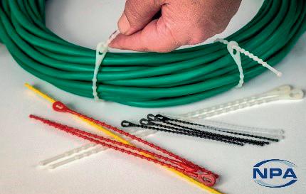
BEADED TIES
NPA beaded ties feature an innovative beaded design that allows for adjustment and reusability, unlike conventional cable ties that require cutting and replacement upon removal. The beaded ties can also be unfastened and adjusted, saving time and resources, and reducing waste. They also keep wires from slipping or sliding due to pulling forces.
The beaded ties are constructed from polyethene to provide greater flexibility, allowing the tie to wrap more tightly around smaller diameters. Polyethene also stays more flexible compared to nylon, which can become rigid and brittle over time. There is also no mechanical release mechanism that can break down or break off. Their one-piece construction is designed to provide consistent performance, while their versatility extends to a broad compatibility with various cable diameters and configurations, accommodating a range of needs and preferences.
The beaded ties combine innovative design and versatility to meet the requirements of cabling professionals. NPA is ISO9001 accredited.
NPA Pty Ltd www.npa.com.au
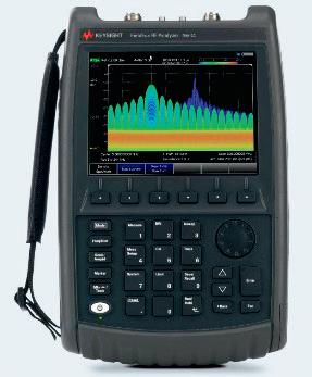
RF ANALYSER
Keysight Technologies has launched the Fieldfox N9912C RF Analyser. The RF analyser is a lightweight and softwaredefined instrument that can be configured for cable and antenna test, vector network analysis and RF power measurement.
Signal analysis is performed with the spectrum analyser option and includes real-time spectrum analysis, interference analysis, EMI pre-compliance and EMF measurements, AM/FM demodulation, 5G and LTE OTA analysis, mapping and more.
The analyser is suitable for users in the field, as it is designed to handle routine maintenance and in-depth troubleshooting. The device is equally at home in the R&D lab or classroom.
All instrument capabilities and options are software licence upgradeable. Frequency bands for each instrument (CAT, VNA and SA) are independent and can be configured at time of order or upgraded separately via a software licence as needs demand to 4, 6.5 or 10 GHz.
Fully upgradable with more than 20 software applications, users can customise the analysis to their requirements. VNA and SA frequencies can be mixed and matched.
The RF analyser is distributed by RapidTech Equipment and will be displayed at Electronex 2024, Stand A1.
14 MAY/JUNE 2024 WWW.ELECTRONICSONLINE.NET.AU
Rapid-Tech
STAND A1 STAND A2
Equipment www.rapid-tech.com.au
SYDNEY 19–20 JUNE 2024 STAND A29

ELECTRONEX SYDNEY 19–20 JUNE 2024
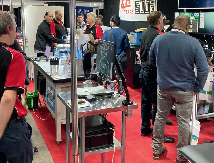
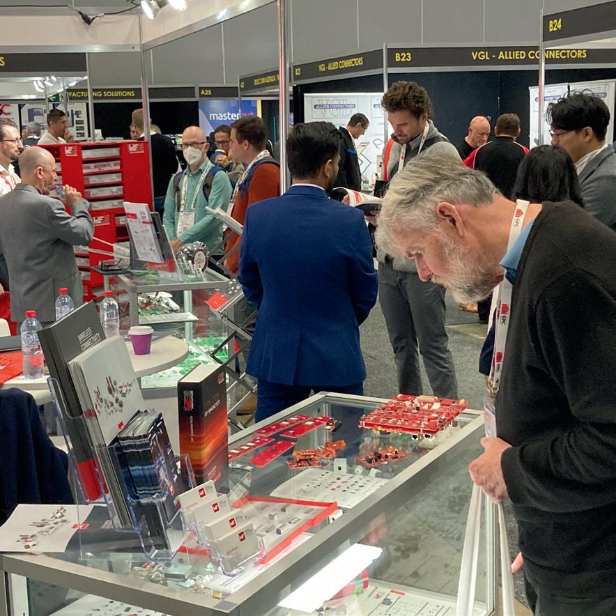
AUSTRALIA’S LARGEST RETURNS TO SYDNEY ELECTRONICS EXPO
Electronex — the Electronics Design and Assembly Expo — will be held at Rosehill Gardens Event Centre from 19–20 June 2024, featuring a vast array of new products and technology for companies using electronics in design, assembly, manufacture and service.
The event was first held in 2010 and this year’s Expo will feature over 100 leading companies and suppliers with the latest innovations and solutions for a range of electronic applications.
Trade visitors will be able to discuss their applications and talk to experts who can assist them in finding the right products and solutions for their business. A post-show survey in Melbourne last year revealed that 96% of visitors said the Expo was beneficial for their industry, 90% found new companies and 85% discovered new products and technology they were not aware of. The SMCBA Electronics Design and Manufacture Conference will be held in conjunction with Electronex and features sessions and technical workshops from international and local experts.
Electronex will feature a range of electronic components, surface mount and inspection equipment, test and measurement and other ancillary products and services, enabling attendees to discuss their specific requirements with contract manufacturers that can design and produce turnkey solutions. The show welcomes designers, engineers, managers, industry enthusiasts and other decisionmakers who are involved in designing or
manufacturing products that utilise electron ics. It is the only specialised event for the electronics industry in Australia. With many Australian manufacturers now focusing on niche products and high-tech applications, the event provides an important focal point for the industry in Australia.
Free seminars and IPC Hand Soldering Competition
A series of free seminars will also be held on the show floor with visitors able to attend on the day with no pre-booking required. These sessions will provide insights into some of the latest product advancements and applications plus case studies of successful onshoring manufacturing in Australia. The full program of seminars can be accessed on the show website.
Following the success of the inaugural hand soldering competition in Melbourne last year, the IPC and SMCBA have joined forces this year to hold the “Australasian Round” of the 2024 IPC Global Hand Soldering Competition with sponsorship from JBC and Oritech. Anyone confident of their hand soldering technique is welcome to compete, with the winner having the opportunity to represent Australasia in the international finals in Munich!
Since 1988 the Surface Mount & Circuit Board Association (SMCBA) has conducted Australia’s only conference dedicated to electronics design and manufacture in conjunction with Electronex. This year’s conference will feature a line-up of local and international experts. David Bergman, Vice President of IPC International, will give the keynote address, ‘Digitalisation of Electronics Manufacturing — Towards Smart Factory enabling Industry 4.0’. Other presenters include Mike Creeden, Founder of San Diego PCB Designs, who will present ‘Three Mutually Required and Competing Perspectives for Printed Circuit Engineering Success: Solvability, Performance, and Manufacturability’; David Hillman, Hillman Electronic Assembly Solutions LLC, will present ‘IMCs: Basic Metallurgy and Impact on Product’; Rick Hartley of RHartley Enterprises topic will present ‘System Mechanical Design to Control EMI’ and Chris Turner, PCBA Test Engineering SME, will discuss ‘Creating an optimal PCBA design and manufacturing process’ and ‘Examples of Design for Test (DFT)’.
Visitors to the expo can register for free at www.electronex.com.au and for details on the soldering competition and conference visit www.smcba.asn.au.
WWW.ELECTRONICSONLINE.NET.AU MAY/JUN 2024 15
iStock.com/peshkov
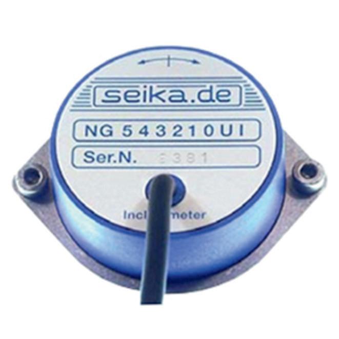
INCLINOMETERS AND ACCELEROMETERS
Control Devices will be showcasing Seika inclinometers and cccelerometers at Electronex 2024.
The Seika sensors are designed for most tilt measurement applications and are Safety Integrity Level 2 (SIL2) rated, making them suitable for a range of safety-related requirements. Sensor housing options are also available for advanced performance opportunities. Control Devices Australia www.controldevices.com.au

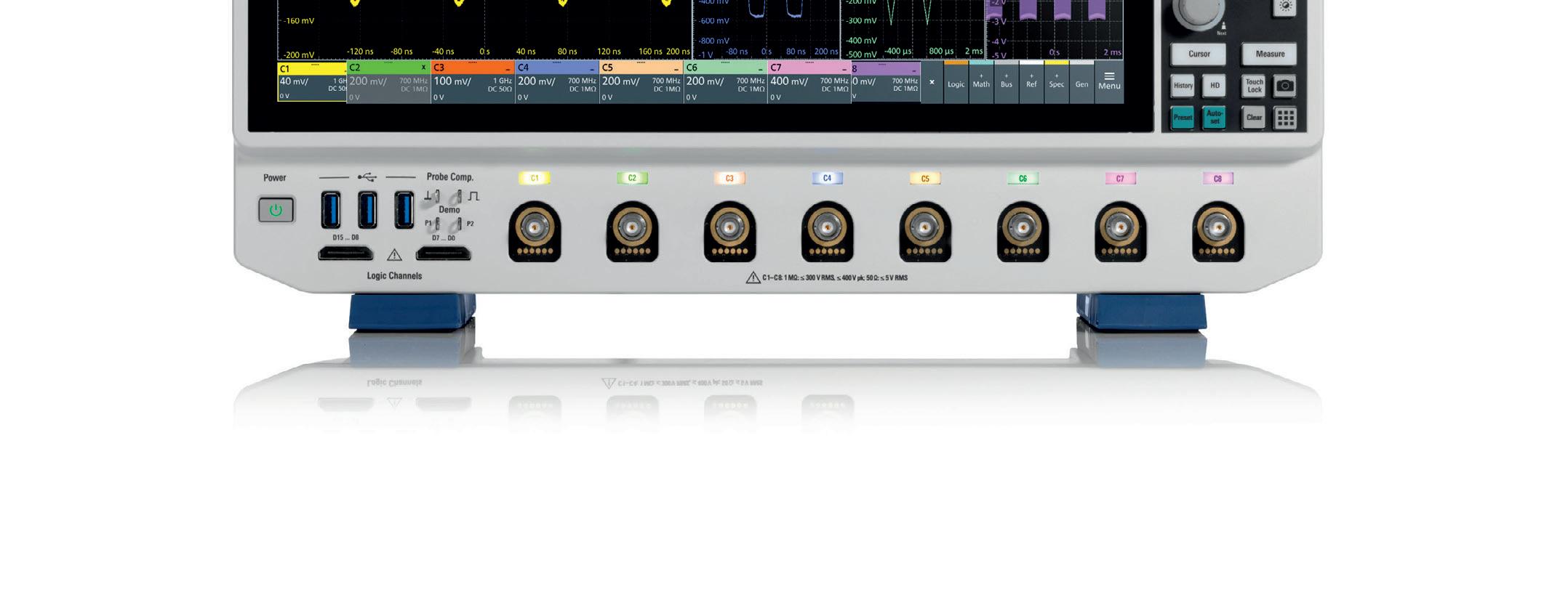
OSCILLOSCOPE
The Rohde & Schwarz MXO 5 series oscilloscope is designed to speed up understanding and testing of electronic systems with four and eight channel models. The oscilloscope facilitates quick acquisitions with multiple channels, maths functions and spectrum measurements for reduced blind time with 21 ns re-arm.
The oscilloscope also enables fast spectrum analysis, with the ability to run up to four analyses simultaneously. Users can also benefit from a deep standard memory and up to one million waveform segments.
The device’s digital trigger features 18-bit HD resolution with adjustable sensitivity to enable triggering. A low noise floor and large vertical offset range of ±5 V at 0.5 mV/div provides enhanced signal fidelity. The oscilloscope also includes a trigger jitter with less than 1 ps.
Rohde & Schwarz (Australia) Pty Ltd www.rohde-schwarz.com.au
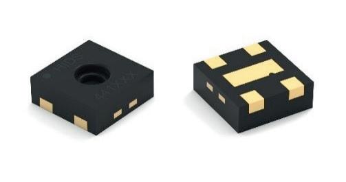
HUMIDITY SENSOR CAPACITOR
Würth Elektronik has launched a compact digital humidity sensor in the WSEN-HIDS series. The MEMS (micro-electro-mechanical system) sensor is designed to conduct measurements within a range of ±1.8% RH in the 20–80% relative humidity range. The DFN (Dual Flat No Leads) package for SMT assembly measures 1.5 x 1.5 x 0.5 mm. The sensor works with a current of 0.4 µA and can be operated with a power supply between 1.08 and 3.6 V. The sensor is suitable for distributed IoT sensor networks, such as those in smart farming applications.
The humidity sensor uses a dielectric polymer that interacts with water molecules to adjust the permeability of the capacitor structure depending on the relative humidity of the surroundings. A temperature sensor is also included. Using the integrated analog-digital converter, the momentary temperature as well as the humidity information can be transmitted as 16-bit measurement data directly to conventional microcontrollers via an I²C interface. The heater (also included) with three selectable heating levels can be switched on as required, to enable the sensor to work under demanding ambient conditions without falsifying measurements due to condensation.
The humidity sensor is suitable for a range of applications, from air-conditioning equipment to data loggers in the food industry, to smart buildings, vertical farming and other applications that require environmental control. To support rapid prototyping, the sensor is part of the FeatherWing sensor and the IoT Development Kit from Würth Elektronik.
Wurth Electronics Australia Pty www.we-online.com
16 MAY/JUNE 2024 WWW.ELECTRONICSONLINE.NET.AU
STAND B10 STAND B14
STAND B16 ELECTRONEX SYDNEY 19–20 JUNE 2024
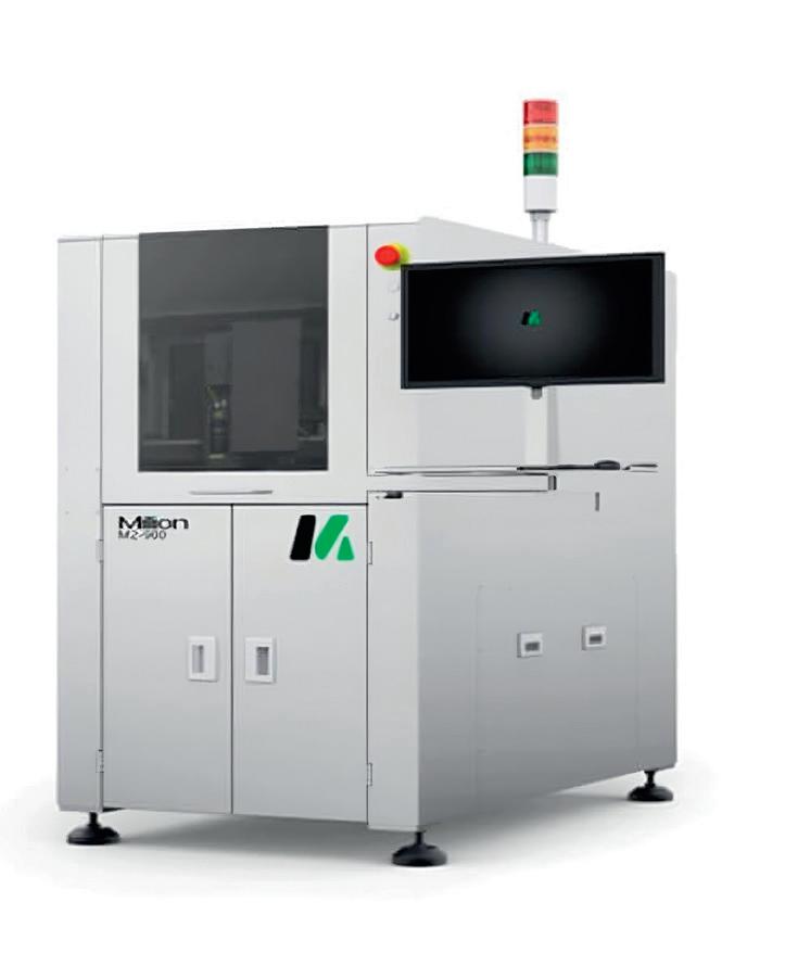
LASER MARKING SYSTEM
The M2-900 laser marking system from SC Manufacturing Solutions is designed to help generate 1D and 2D codes, text, logos and optical characters. The system features four types of lasers (CO2, UV, green and fibre) to enhance performance. The laser marking system features a support top and bottom dual-headed configuration for greater flexibility and throughput, while the standard dual-camera configuration facilitates simultaneous reading and marking. The device is also equipped with fume detection and a safety enclosure with interlock switches to prevent pollution of the shop floor. An optional dual conveyor configuration also provides high throughput. The standard configuration also features a separate dust collector.
SC Manufacturing Solutions Pty Ltd www.scmsau.com


WWW.ELECTRONICSONLINE.NET.AU MAY/JUN 2024 17
STAND D28 ELECTRONEX SYDNEY
2024
19–20 JUNE

JOHN HOLLAND EMPLOYS ASSET TRACKERS FOR SPOIL MANAGEMENT
DIGITAL
MATTER’S
NORDIC NRF9160SIP-POWERED OYSTER3 AND REMORA3 FROM THE BASIS OF JOHN HOLLAND’S SPOILTRAC SYSTEM
With over 600 million tons of construction and demolition waste generated in the U.S. in 2018 alone (according to the Environmental Protection Agency (EPA)), proper disposal is crucial. And it’s not just the spoil volume — the wide variety of waste types, from inert to hazardous, present serious logistical challenges for construction firms trying to adhere to the strict and regulated demands for disposal or recycling.
Having clear records of the amount and type of spoil, and where it has been discarded, can help companies avoid fines. Any mistakes can be costly — the EPA, for example, recently tripled the maximum fines for improper disposal to over $70,000 per day in California.
“Conventional processes for spoil tracking are labor intensive, time consuming and carry with them considerable risks of delay, overcharging, illegal spoil dumping and missed spoil re-use opportunities,” says Fazil Hassan, Digital Development at Australian construction company John Holland.
To combat these problems, John Holland has implemented its award-winning SpoilTRAC system to monitor the movement of construction site waste — from extraction all the way to disposal. Based on IoT technology company Digital Matter’s Oyster3 and Remora3 battery-powered geolocation asset tracking devices, this solution features an IP67-rated weatherproof, ultra-rugged housing to help protect it from extreme conditions while mounted on dump trucks.
The wireless operation of SpoilTRAC allows for easy installation, removal and transfer between vehicles. This flexibility is important in construction projects, which often involve multiple subcontractors with their own kit.
Outfi tted with an on-board temperature sensor and threeaxis accelerometer for movement detection, high-G events and rotation counting, the Oyster3 and Remora3 can also identify when the truck’s tray has moved into the predetermined tilt position, indicating that the spoil has been discarded.
18 MAY/JUNE 2024 WWW.ELECTRONICSONLINE.NET.AU SPONSORED CONTENT
By facilitating overall waste management, the platform encourages spoil reuse across projects, optimizes plant and personnel utilization, and presents opportunities for enhanced sustainability outcomes.
Reliable asset monitoring
Employing Nordic’s nRF9160 SiP, the Oyster3 and Remora3 devices combine cellular network location data with GPS trilateration to precisely locate each disposal truck. The devices complement GPS with cell tower location fallback when GPS signals are unavailable. The nRF9160 SiP’s LTE-M/ NB-IoT modem can then transmit the truck’s location to the SpoilTRAC platform.
This platform offers detailed information on the spoil category of each load, accompanied by a map illustrating loading and unloading points. Because construction sites and licensed landfills are geofenced and tagged with the classification of refuse, if a contaminated load is dropped in the wrong location an illegal dumping alert is triggered.
By facilitating overall waste management, the platform encourages spoil reuse across projects, optimizes plant and personnel utilization, and presents opportunities for enhanced sustainability outcomes. Additionally, the use of cellular connectivity to transfer data to the platform ensures robust coverage while trucks are on the move.
“The cellular functionality of the nRF9160 made it easier to build a solution, as the amount of upload and download data is not constrained to the same extent as other LPWAN tech,” explains Ken Everett, CEO at Digital Matter.
Need to Know
The Nordic nRF9160 offers excellent low power cellular operation, caters for both LTE-M and NB-IoT, and allows Digital Matter to put its application code on to the SiP, thereby doing away with the need for an external microcontroller.

“[For example], the Remora3 is capable of ‘second-by-second’ [near real-time] tracking — which is unique on a battery-powered device — to support extended aggressive reporting requirements including highly accurate speed reporting, as well as run hour and odometer monitoring on mobile assets,” explains Everett.
“The solution is perfect for any asset which requires aggressive long-term tracking with ‘low touch’ requirements — for example, tracking heavy machinery that doesn’t have an easily accessible power source,” says Everett.
Further advantages
Beyond providing the robust connectivity for efficient data transfer, the Nordic nRF9160 SiP delivers further advantages to the Digital Matter solutions.
“It also allows us to manage and update the devices in the field. We provide over-the-air firmware updates as well as other device management functions,” says Everett.
Battery life was also a critical factor when selecting the Nordic SiP, according to Everett. “Extending product lifetime significantly reduces operational costs for businesses — and eliminates the logistical nightmare of sourcing and coordinating battery changes, especially across large deployments,” he explains.
The Oyster3 tracker boasts a battery life of up to ten years with daily position updates, or seven years with movement based location updates, and issues alerts when the battery level is low. The Remora3 features a “deploy once” battery life allowing it to perform typical movement-based tracking for over ten years.
“Digital Matter went through an extensive analysis of competing cellular modems and decided on the nRF9160 due to its feature set and, most importantly, the very low power operation,” adds Everett. “Nordic has done an excellent job in achieving the lowest power levels of all modules evaluated.”
Nordic Semiconductor www.nordicsemi.com
WWW.ELECTRONICSONLINE.NET.AU MAY/JUN 2024 19
iStock.com/ugurhan
ELECTRONEX SYDNEY
PUSH-BUTTON SWITCHES
Altronic Distributors has added dual-colour push-button switches to its range of switching componentry. The switches offer a high level of vandal resistance for use in high-risk environments in equipment such as ticket and vending machinery.
With an IP65 rating, the switches are dust-tight and water protected, making them suitable for both indoor and outdoor applications, even in challenging environmental conditions. The versatile SPST configuration makes them suitable for a range of applications, from industrial machinery control to security systems.
The switches also offer dual LED colour status to facilitate clear feedback during use. The switch range is designed to be secure and durable, with a high level of visual appeal.
Altronic Distributors Pty Ltd www.altronics.com.au
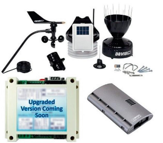
WEATHER STATION GATEWAY
The Ocean Controls KTA-382 weather station gateway offers an updated gateway replacement for the Davis weather stations, namely the Vantage Pro and the Vantage Pro 2. The updated model provides various new features for ease of operation, as well as additional functionality. The base functions and the dimensions of the KTA-282 and GWY-141 have also progressed through to the new model, to facilitate an easier upgrade.
New features of the weather station gateway include a Wi-Fi access point with fully user-configurable connection capability, with a custom webpage. The device also features two simultaneous and independent serial ports — capable with Modbus RTU (1x Db9/USB-C + 1x RS485). These ports offer individually manipulable serial settings (such as baud and parity), without the need for a power cycle.
The gateway also features a data-logging variant that supports micro-SD cards, along with a PoE (Power over Ethernet) variant. Users can also access direct cloud support for Weather Underground, with custom cloud support available on request. The device also comes with a proprietary PC application for desktop monitoring or troubleshooting and two digital I/Os (including a custom alarm setting).
The KTA-382 will provide continuous support for further developments and envoys from Davis Instruments, and offers a streamlined gateway solution for the Davis product line. Ocean Controls www.oceancontrols.com.au

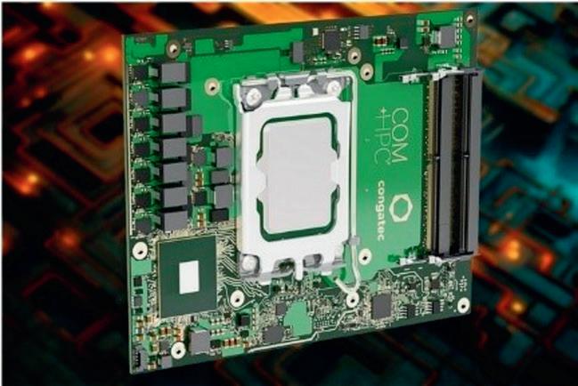
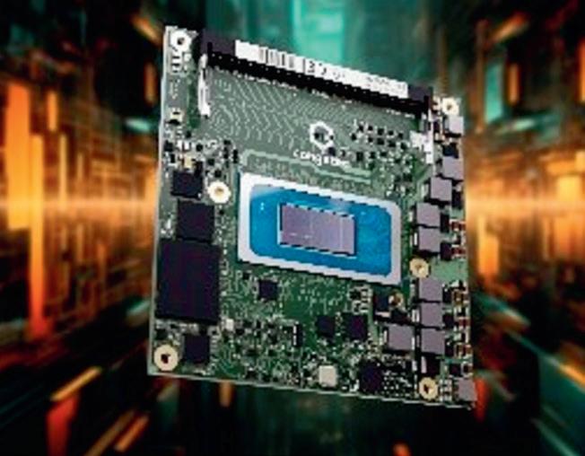
COMPUTER-ON-MODULES
congatec has introduced four high-end COM-HPC computer-on-modules, based on the 14th Generation Intel Core processors (codename Raptor Lake-S Refresh).
Representing an extension to the existing conga-HPC/ cRLS computer-on-modules, the modules are suitable for industrial workstations and edge computers. With Intel’s improved production quality, clock frequencies have been increased, resulting in performance gains across the entire range. The Intel Core i7-14700 processor-based modules feature four additional E-Cores compared to the Intel Core i7-13700E variants, providing an additional performance boost with 20 cores in total. Another new feature is the improved bandwidth of USB 3.2 Gen 2x2 with up to 20 Gbps.
The COM-HPC Size C form factor (120 x 160 mm) addresses application areas that require enhanced multi-core and multi-thread performance, and large caches combined with high bandwidth and advanced I/O technology. The target markets for the computeron-modules include industrial automation and medical technology as well as edge and network infrastructure applications. They all benefit from the optimised computing cores of this hybrid performance architecture, which currently supports up to 8 performance cores and 16 efficiency cores. Congatec Australia Pty Ltd www.congatec.com
20 MAY/JUNE 2024 WWW.ELECTRONICSONLINE.NET.AU
STAND A2 STAND D13 STAND A16
19–20 JUNE 2024


Researchers at the Indian Institute of Science (IISc) have developed flexible films that exhibit bright colours purely by virtue of their physical structure, without the need for any pigment. When stretched, the films exhibit a change in colour as a response to the mechanical deformation.
To design these films, the team devised a novel cost-effective and scalable single-step technique that involves evaporating gallium metal to form nano-sized particles on a flexible substrate. Their method allows the simultaneous fabrication of multiple structural colours responsive to mechanical stimuli.
The team has also shown how these films can be used for a variety of applications, from smart bandages and movement sensors to reflective displays.
“This is the first time that a liquid metal like gallium has been used for photonics,” said Tapajyoti Das Gupta, Assistant Professor in the Department of Instrumentation and Applied Physics (IAP) and corresponding author of the study published in Nature Nanotechnology
Some natural objects like gemstones, mollusc shells or peacock feathers are inherently colourful. Their colours emerge from the interaction of light with micro- or nano-structures arranged periodically, such
as tiny silica spheres in opal, calcium carbonate-based platelets in mollusc shells and segmented ribbons atop cylindrical structures in peacock feathers.
Nature-inspired structurally coloured materials have found broad applications in displays, wearable electronics, visual sensors and anti-counterfeiting tags. In recent years, scientists have been trying to design materials which can change colour in response to an external mechanical stimulus.
The IISc team began experimenting with gallium, which has not been explored for such applications because its high surface tension hinders the formation of nanoparticles. Gallium is a liquid metal at room temperature and its nanoparticles have been shown to
22 MAY/JUNE 2024 WWW.ELECTRONICSONLINE.NET.AU
Sankeerthana Avasarala, Indian Institute of Science

have strong interactions with electromagnetic radiation. The process developed by the team achieves the feat of overcoming the barrier of surface tension to create gallium nanoparticles, by cleverly using the properties of a substrate called polydimethylsiloxane (PDMS), a biocompatible polymer.
When the substrate was stretched, the researchers noticed something unusual. The material started showing different colours depending on the strain. The researchers theorised that the array of deposited gallium nanoparticles interacts with light in specific ways to generate the colours.
To understand the role of the substrate in colour generation, the team developed a mathematical model.
“We show that the PDMS substrate not only holds the structure, but also plays an active role in determining the structure of gallium nanoparticles and resulting colouration,” said Renu Raman Sahu, PhD student in IAP and lead author. Even after 80,000 cycles of stretching, the material was able to show a repeatable colour change, indicating its reliability.
Conventional techniques such as lithography used to fabricate such materials involve many steps and are costly to scale up. To circumvent this, the team devised a singlestep physical vapour deposition technique to evaporate the liquid gallium metal and deposit it on the PDMS substrate. This allowed them to fabricate flexible, structurally coloured films measuring about half the size of a palm.
PDMS is a polymer made by mixing two liquid-like components — an oligomer and a cross-linker — which react with each other to form a solid polymer. What the researchers found is that the unreacted portion of oligomer, which is still in a liquid state, played a crucial role in stabilising the formation of gallium nanoparticles on the substrate. When this substrate is then stretched, the liquidlike oligomers seep into the gaps between the nanoparticles, changing the gap size and their interaction with light, resulting in the observed change in colouration. Experiments carried out in the lab confirmed the model’s predictions. By tuning the ratio of the oligomer content to the cross-linker, the researchers obtained a gamut of colours.
There are various applications possible for such films. The team demonstrated one such application: a body movement sensor. A strip of the film, when attached to the finger, changed colour when the finger was bent, helping to sense movement in real time. “In the future, these materials could be used for energy-harvesting applications as well,” Sahu said.
Sahu RR, Ramasamy AS, Bhonsle S, Vailshery M, Archana S, Kumar H, Das Gupta T, Single-step fabrication of liquid gallium nanoparticles via capillary interaction for dynamic structural colours, Nature Nanotechnology (2024).
Sahu RR, Das Gupta T, Fabrication of mechanochromic gallium nanostructures by capillary interactions, Nature Nanotechnology (2024).
Sahu RR, Ramasamy AS, Gap-plasmonic tuneable structural colors by capillary interactions.
WWW.ELECTRONICSONLINE.NET.AU MAY/JUN 2024 23
Sample exhibiting colour change from pink to green on local application of force with a tweezer tip.
From left to right: Tapajyoti Das Gupta, Renu Raman Sahu, Mark Vailshery and Alwar Samy Ramasamy.
Alwar Samy Ramasamy, Indian Institute of Science.
NANOMATERIALS
Renu Raman Sahu, Indian Institute of Science.
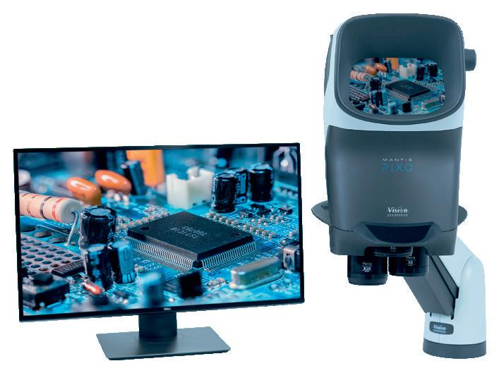
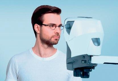
MICROSCOPE
Hawker Richardson has unveiled a new series of microscopes: the Mantis PIXO, Mantis ERGO and Mantis IOTA. All three models provide 3D images in an easy-to-use ergonomic design.
The Mantis microscopes are designed with an eyepiece-less viewer so users can wear prescription glasses. As users don’t need to align their eyes precisely, they can view subjects easily, without having to move their heads. The Mantis also provides long working distances under lenses so users can do rework while looking at subjects under magnification, thereby improving efficiency.
The microscopes offer 5-way illumination for control over lighting to achieve shadow-free inspection. The PIXO microscope features a 3-lens turret so users can scroll through magnifications easily, thereby increasing productivity with magnification up to 15x. The integrated high-definition 5 MP camera on the PIXO enhances image quality and provides greater colour reproduction. With the video and image capture software feature, users can also record, review and share resources for traceability, collaboration and training.
All models accommodate the two new stands; the Stabila offers a long range of improved focus travel from 55 to 150 mm focus while the Verso arm has an increased max reach over the previous models, now being 755 mm.
The Mantis microscopes are suitable for high-value, performance-critical micro-PCB work where components need to be soldered onto a baseboard. The PIXO Mantis head can also be set up with the multi-turret lens fixture to enable quick changes of magnification. The microscope also offers white/UV illumination for applications such as conformal coating validation on printed circuit boards, for even coverage. Users can also change from one light to another to view the coating itself.
Check out the Mantis PIXO with the integrated digital camera and Stabila stand at the Hawker Richardson stand at Electronex. Hawker Richardson www.hawkerrichardson.com.au

DATA LOGGER
ATI has launched the HIOKI LR8450 Hilogger data logger, paired with the HIOKI AC/ DC current sensors (CT7812 and CT7822). Efficient power management is crucial for electric vehicles, to increase their range. Therefore, it is important to measure power consumption and current leakage across various components.
The LR8450 data logger is designed to simultaneously measure and record current consumption and leakage across multiple channels, making it suitable for both manufacturers and researchers. Supporting up to 330 channels enables the data logger to record data from both the battery and the Controller Area Network (CAN bus), thereby providing integrated analysis of vehicle states and current consumption profiles. For more complex EV testing, users can utilise the LR8450 wireless measuring unit, to reduce complex wiring and minimise loss of data.
ATI Australia Pty Ltd www.ati.com.au

24 MAY/JUNE 2024 WWW.ELECTRONICSONLINE.NET.AU
STAND A20 STAND B32 ELECTRONEX SYDNEY 19–20 JUNE 2024
DIGITAL OSCILLOSCOPES
Emona Instruments will be demonstrating the Rigol DHO-800 and DHO900 series of digital oscilloscopes at Electronex. The DHO800/900 series is designed to be portable, weighing 1.7 kg and with a diameter of 78 mm. The series features 12-bit resolution, a capture rate up to 1,000,000 wfms/s (in UltraAcquire Mode), 25 and 50 Mpts of memory depth and an enhanced low noise floor.
The oscilloscopes also offer a 7 ″ (1024x600) capacitive multi-touch screen and a Flex Knob user-friendly experience. Additionally, USB Device & Host, LAN and HDMI interfaces are standard for all models of this series.
The DHO-900 series also supports 16 digital channels. One instrument can make an analysis on both analog and digital signals to meet the embedded design and test scenarios. Users can also access auto serial and parallel bus analysis, bode plot analysis and other functions to meet test demands in R&D, education and scientific research.
Emona Instruments Pty Ltd www.emona.com.au


WWW.ELECTRONICSONLINE.NET.AU MAY/JUN 2024 25
STAND B2 ELECTRONEX SYDNEY 19–20 JUNE 2024

FREQUENCY ANALYSER
Pendulum Instruments has launched the CNT-102 dual-channel frequency analyser. Expanding Pendulum’s multi-channel frequency analyser (MFA) family, the CNT-102 supports parallel and independent time/frequency measurements in a bench-top format. The frequency analyser features several key capabilities, including simultaneous and gap-free Frequency, Period, Time Interval Error, Pulse Width, Rise/Fall time, Slew Rate, Totalise and Voltage measurements. The standard frequency range is up to 400 MHz and an optional RF input extends bandwidth up to 24 GHz.
The multi-channel design enables a multitude of new test applications, most notably parallel frequency measurements of two different test objects, or the comparison of pulse parameters between two parallel test points, without having to swap over test leads.
The frequency analyser also features 14ps time resolution and up to 13 digits/s frequency resolution. A large colour touch screen and intuitive graphic user interface display results in both numeric and graphic formats, along with modulation/trend and value distribution graphs. Advanced analysis enables smoothing of data and zooming functions with cursor read-outs of individual samples.
Multi-channel frequency analysers are suitable for many test systems requiring multiple frequency counters such as oscillator manufacturing, since a single CNT-102 can replace two traditional counters in a test rack, resulting in both space- and cost-saving.
Rapid-Tech Equipment
www.rapid-tech.com.au
CLEANING AND DE-FLUXING SOLVENT

The AB Chimie SND Cleaning and De-Fluxing Solvent is a fast-drying cleaning solvent that is designed to remove grease, oil, flux residue and acrylic conformal coatings from PCBs. This 100% ozone-friendly solvent is suitable for a range of cleaning requirements.
The non-CFC and non-halogenated cleaning solvent leaves no greasy residues after evaporation and is harmless to most plastics, rubbers, elastomers and surface coatings. The cleaning solvent is available in convenient cans and in bulk options.
SND is suitable for a range of applications. It is designed to efficiently remove coatings from PCBs, with a special ability to dissolve acrylic varnish. Its compatibility with various plastic materials also enhances its versatility.
Onboard Solutions
www.onboardsolutions.com.au
MASS FLOW CONTROLLER
The Sensirion SFC6000D mass flow controller is small and light and therefore allows the customer to optimise their devices in terms of size and weight. This is a decisive advantage, especially for portable devices. The mass flow controller also offers good performance in terms of repeatability, control range and speed. The controller is highly integrated and has a robust supply chain due to the low number of electronic components used. Sensirion has designed the radical mass flow controllers using CMOSens MEMS technology, based on the thermal-mass measurement principle.
Glyn Ltd
www.glyn.com.au
DIODES
The Questsemi silicon carbide (SiC) Schottky diodes developed by Queensland Semiconductor Technology Pty Ltd (Questsemi) are a key element in many power conversion systems. Due to their thermal conductivity, high switching performance and efficiency, the diodes are like solar inverters, motor drives, electric vehicle (EV) chargers and uninterruptible power supplies.
The diodes could improve the overall cost of the semiconductor devices used in energy-efficient technologies. The SiC Schottky diodes are designed to play a role in the semiconductor value chain, with a flow-on effect in the design, prototyping and fabrication of other semiconductor devices.
Qld Semiconductor Technologies https://questsemi.com
26 MAY/JUNE 2024 WWW.ELECTRONICSONLINE.NET.AU
STAND A1
STAND C21 STAND D36
STAND A32
19–20 JUNE 2024
ELECTRONEX SYDNEY
WHY SEHO SELECTIVE SYSTEMS ARE CHANGING THE WAY MANUFACTURERS SOLDER BOARDS USING THROUGH HOLE DESIGNS

While a lot of manufacturers are benefitting from board designs utilising surface mount technology (SMT), some boards can only ever use Wave and Selective technologies. This article looks at some of the best solutions on the market for Soldering through hole boards from SEHO and why some of the technology they’ve employed could be a game changer for manufacturers requiring Wave and/or Selective solutions.
Who are SEHO?
Founded in 1976, SEHO are world leaders in solder systems, with locations in the USA, South Korea, and China, in addition to their headquarters In Germany.
SelectLine-C – Award-winning mid-range modular system
The SelectLine is ideal for growing organisations because the modular system can increase its capability as your organisation’s production grows. The standard configuration consists of a base module and controller, and it can be retrofitted with additional features either from the factory or later. Features include automated optical inspection (AOI), brush for reducing maintenance, gold nozzles for greater longevity.
The SelectLine can be run in a couple of modes: Chaotic mode (Running board A and then B behind it and then C etc.) So, running one board and then another rather than batch building; Synchro mode - with two solder pots for greater speed i.e. one solder pot does one half of the board, and the other solder pot does the other half to increase throughput.
SEHO design and manufacture their soldering solutions in Germany and the offering consists of both Wave and Selective solutions for soldering which range can be utilised or inline production or standalone including:
Greater flexibility – high-mix, high volume. SEHO soldering systems are designed to increase efficiencies as well as provide greater fl exibility, allowing users to confi gure the systems for providing multiple processes.
Minimising maintenance and downtime – crucial for wave and selective solutions because maintenance tends to be more a costly and time-consuming process compared to reflow. However, SEHO spend a lot of time investing in their R&D and so deliver systems designed to clean at regular intervals, so that it doesn’t impact production but helps to prevent build-up of solder deposits.
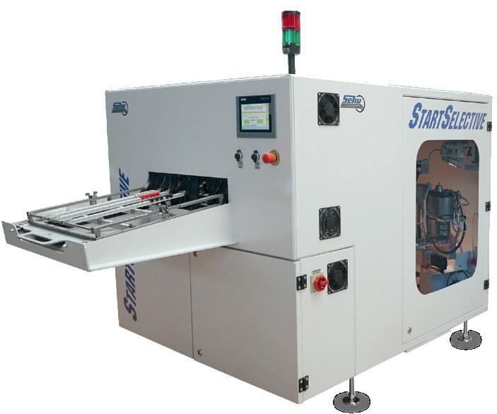
What makes SEHO’s soldering solutions unique?
The SEHO systems are designed with a range of patented technological advances. One important feature which can ensure repeatable quality and improve cycle times is the integrated automated optical inspection (AOI) system. The AOI can be stationary mounted in the production cell or installed on a separate access so there is no impact on cycle time.
Is there support and maintenance for SEHO solutions in Australia and New Zealand?
Hawker Richardson have recently sold a SEHO solution to a contract manufacturer who are still running their SEHO they purchased twenty-fi ve years ago. Investing in a good quality product over cheaper alternatives pays back in the long run. Hawker Richardson keeps a large range of spares in their warehouse and with a large, dedicated service team, they can support customers with both repairs and maintenance anywhere in Australia and New Zealand. The systems can also be accessed remotely so initial support can be provided quickly to minimise downtime.
Hawker Richardson is the authorized distributor for SEHO Systems GmbH in Australasia.
WWW.ELECTRONICSONLINE.NET.AU MAY/JUN 2024 27 SPONSORED CONTENT
Richardson www.hawkerrichardson.com.au
Hawker
iStock.com/anyaivanova
Hawker Richardson
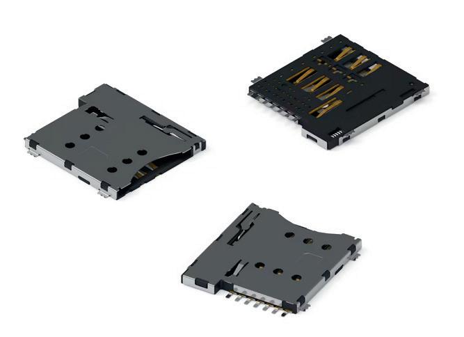
SIM CARD CONNECTOR
Würth Elektronik has expanded its range of card interfaces with the WR-CRD Micro SIM Card Connector with ‘Push & Push’ insert and eject mechanism.
The SIM card receptacle is designed to be kink-resistant and durable to enable card detection. The brass contacts are gold-plated and the package is made of tin-plated steel. The contact resistance is approximately 100 m Ω. The operating temperature range is -20 to +70°C. The WR-CRD Micro SIM Card Connector is now available from stock.
Wurth Electronics Australia Pty www.we-online.com
SOLDER PASTE
The Interflux DP5505 solder paste is made in Australia by Oritech. The solder paste is designed for a range of applications and offers stability under different temperature and humidity conditions. The solder paste is designed to simplify post-solder cleaning processes, as it features a no-clean formula, leaving components residue-free and ready for the next stage of assembly.

Crafted from an SAC305 alloy with T4 ball size, the solder paste helps to boost the longevity of the user’s electronic connections. The solder paste is versatile and suitable for professionals and hobbyists alike, whether they are working on circuit boards, electronic components or DIY projects.
The solder paste also comes in a user-friendly consistency for easy application, thereby reducing the chance of errors.
Oritech Pty Ltd www.oritech.com.au
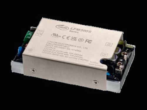
SEMI-POTTED POWER SUPPLY
The Cincon LFM300S series is a 1 ″ low profile 300 W AC-DC semi-potted power supply with an input range of 85–264 VAC, and output voltages of 12, 15, 24, 28, 30, 48 and 54 VDC. In addition, the series meets over voltage categories OVC II and OVC III. The power supply also features OCP, OVP and OTP full protection, along with continuous short circuit protection. It is designed to achieve efficiency to 94% with no load power consumption (less than 0.3 W). The power supply can operate in a range of temperatures, from -40–80°C, and is also IEC/ UL/EN 62368-1 ed.3 approved.
The power supply is suitable for a range of applications, including automation equipment, network and telecom devices, test and measurement instrumentation, display systems, inspection systems and various industrial electronics. Glyn Ltd www.glyn.com.au
& Handles
• Hole Pugs & Bushes
• LED Mounts & Light Pipes
• Cable Ties & Mounts
28 MAY/JUNE 2024 WWW.ELECTRONICSONLINE.NET.AU
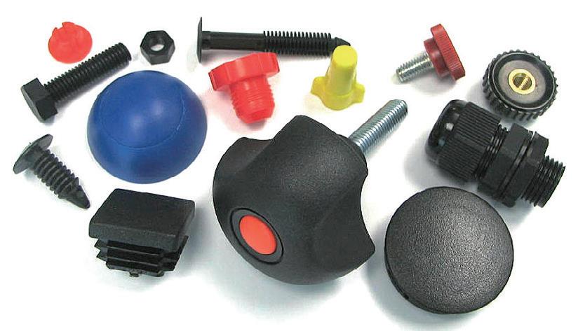
STAND B14 Limited Electronics Hi-Q from Available sales@hiq.co.nz NZ 0800 800 293 www.hiq.co.nz We Stock 1000’s of Plastic Parts for Industry • Nylon Fasteners • Screws & Nuts • Washers & Spacers • Rivets & Clips • PCB Hardware • Caps & Plugs • Knobs
STAND A32 STAND D18
19–20 JUNE 2024
ELECTRONEX SYDNEY

BRAIDED CABLE WRAP
NPA’s innovative self-closing braided cable wrap is designed to be versatile, durable and easy to use. The braided cable wrap features a self-closing mechanism to facilitate installation and removal without the need for additional tools or fasteners. The split open design allows easy install on cables that have already been assembled, and additional cables can easily be added.
The large expansion range of the braided mesh means it can accommodate a range of cable diameters, configurations and irregularities, providing a customised and snug fit for various applications. This adaptability makes it suitable for organising and securing cables of different types and sizes, promoting efficiency in any set-up.
Once in place, individual wires may be passed through the sleeving to allow for breakouts at any point along the length of the harness.
The wrap is made of polyester with an operating temperature of -50–150°C and is halogen free with a certified flammability rating of UL94 V-2.
NPA Pty Ltd www.npa.com.au
Format: 180 x 135 mm


WWW.ELECTRONICSONLINE.NET.AU MAY/JUN 2024 29
Explore Technical Insights
STAND A29 ELECTRONEX SYDNEY 19–20 JUNE 2024
ELECTRONEX SYDNEY
19–20 JUNE 2024
MICROSCOPE
The Hawker Richardson Mantis PIXO, Mantis Ergo and Mantis IOTA microscopes are designed to provide 3D images in an easy-to-use ergonomic design. The Mantis microscopes enable users to wear glasses; unlike other binocular microscopes, the Mantis is designed with an eyepiece-less viewer, so users can wear prescription glasses.
The microscopes also provide long working distances under lenses so users can do rework while looking at their subject under magnification, thereby improving efficiency.
The new generation of microscopes offers 5-way illumination to facilitate control over lighting, to achieve shadow-free inspection. The field of view is also 10% larger for better control over movements when working under the system.
The ERGO microscope features a 3-lens turret so users can scroll through magnifications, thereby increasing productivity with magnification up to 15x. All models accommodate the two new stands; the Stabila offers a long range of improved focus travel from 55 to 150 mm focus while the Verso arm has an increased max reach over the previous models, now being 755 mm.
The microscope is suitable for high-value, performance-critical microPCB work where users need to solder components onto a baseboard. The microscope can also be set up to get the maximum amount of space without losing image quality.
The ERGO microscope offers White/UV illumination for applications such as conformal coating validation on printed circuit boards to facilitate even coverage. Users can also change from one light to another to view the coating itself. Improved hand-eye coordination and lower operator fatigue make tasks such as soldering, PCB inspection and rework easy for extended periods.
Check out the Mantis ERGO microscope and the Mantis IOTA with the Verso arm at the Hawker Richardson stand at Electronex. Hawker Richardson www.hawkerrichardson.com.au
VAPOUR DEGREASER
COMPUTER-ON-MODULES
The conga-TC700 COM Express Compact computer-onmodules with Intel Core Ultra processors (code named Meteor Lake) are power-efficient x86 client SoCs. The computer-on-modules feature up to 6 P-Cores, up to 8 E-Cores and 2 Low Power E-Cores, supporting up to 22 threads, making it possible to consolidate distributed devices onto a single platform. The SoC-integrated Intel Arc GPU with up to 8 Xe Cores and up to 128 EUs can handle graphics up to 2x 8K resolution and ultra-fast GPU-based vision data (pre)processing. The integrated NPU Intel AI Boost is designed to efficiently execute machine learning algorithms and AI inferences.
The computer-on-modules also feature up to 96 GB DDR SO-DIMM with in-band ECC at 5600 MT/s, facilitating high data throughput and low latency.
The modules are supported by congatec’s OEM solution-focused high-performance ecosystem, including efficient active and passive cooling solutions and ready-to-use evaluation carrier boards. The modules can be ordered with pre-evaluated real-time hypervisor technology for virtual machine deployments and workload consolidation in edge computing scenarios. The modules are also suitable for running demanding AI workloads at the edge.
Congatec Australia Pty Ltd www.congatec.com
The Sonictron VP 250/350 M is a vapour degreaser for multipurpose cleaning, designed to remove oil, grease, flux residue and particles. Compact, scalable and environmentally friendly, this vapour degreaser is suitable for small to medium production runs to remove contamination in short cycle times.
The vapour degreaser features two SUS 304 stainless steel tanks with heated control. It also comes with two ultrasonic power sensors, a tank sensor, a molecular water separator and a freeboard cooling coil. The vapour degreaser also comes with one HP single chiller system design.
The low surface tension liquid has high penetration power and good cleaning and rinsing performance.
Onboard Solutions www.onboardsolutions.com.au
30 MAY/JUNE 2024 WWW.ELECTRONICSONLINE.NET.AU
STAND B32 STAND A16
C21
STAND
MODULE
ADLINK Technology Inc. has launched the cExpress-ASL computer-on-modules based on Intel Atom processors, offering up to 8-core CPU at 6/9/12 W TDP. The module utilises Intel’s Gracemont architecture, with broadened cache and memory bandwidth and responsive coding footprint. The module also features a soldered-down memory and extreme temperature option, thereby enabling it to enhance efficiency for wide-ranging IoT solutions at the edge.
The module offers a 2/4/8-core Intel Atom x7000RE and x7000C series processor, with up to 3.8 GHz and up to 16 GB LPDDR5 memory. The module is also integrated with Intel UHD graphics with up to 32 execution units. Along with support for two digital display interfaces (DisplayPort/HDMI), eight PCIe x1 Gen3 lanes, 2.5GbE LAN and USB 3.2, it is suitable for applications including industrial automation, industrial HMI, robotics, AI and more.
The module is also equipped with Intel TCC (Time-Coordinated Computing) and TSN (Time Sensitive Networking) support. Intel TCC facilitates time synchronisation and CPU/IO timeliness within a system, while TSN enhances time precision for synchronised networking between multiple systems.
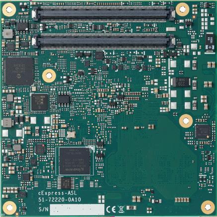
The module is built for highly responsive on-device AI execution and can also withstand ruggedised use scenarios. ADLINK Technology Inc
www.adlinktech.com
BUTTONINTEGRATED PANEL PC
Backplane Systems Technology has launched the APLEX ABOS-916CP, a 15.6 ″ panel PC designed for the evolving needs of smart manufacturing and industrial applications. Powered by the 11th Gen Intel Core i processor, it is designed to provide enhanced performance and efficiency. The panel PC features built-in RAFI FS22+ functional buttons, including real push-buttons that enhance user interaction by providing intuitive control over complex processes.

Crafted for the modern industrial environment, the panel PC integrates a Full HD TFT LED LCD with projected capacitive touch technology, providing clear visuals and responsive touch interaction. This panel PC is built to withstand harsh conditions, featuring an IP65 fully sealed, anticorrosion enclosure, gap-free sealing and a slim front frame architecture that offers protection against environmental elements.
The ABOS series is equipped with default buttons for start, stop and reset, along with three customisable buttons for tailored operations. It also includes an emergency button and a key switch for added safety and security, to enable operations to be halted immediately in critical situations.
For connectivity, the ABOS-916CP is equipped with 1 x USB 2.0 on the front panel for easy access, supporting 4 x USB 3.2, 2 x LAN, with options for 2 x COM and 8-bit GPIO, making it a versatile choice for a range of industrial applications. Its aluminium enclosure and stainless steel I/O cover, capable of withstanding the rigours of industrial environments, alongside flexible mounting options, make the ABOS916CP suitable for smart factories, process control, CNC machines and robotic arms, enhancing productivity and reducing human error in smart manufacturing settings.
Backplane Systems Technology Pty Ltd www.backplane.com.au

WWW.ELECTRONICSONLINE.NET.AU MAY/JUN 2024 31
BRAININSPIRED SYSTEM GATHERS DATA FROM SALT-SIZED SENSORS
Brown University
Tiny chips may equal a big breakthrough for a team of scientists led by Brown University engineers.
Writing in Nature Electronics, the research team describes a novel approach for a wireless communication network that can efficiently transmit, receive and decode data from thousands of microelectronic chips that are each no larger than a grain of salt.
The sensor network is designed so the chips can be implanted into the body or integrated into wearable devices. Each submillimetre-sized silicon sensor mimics how
neurons in the brain communicate through spikes of electrical activity. The sensors detect specific events as spikes and then transmit that data wirelessly in real time using radio waves, saving both energy and bandwidth.
“Our brain works in a very sparse way,” said Jihun Lee, a postdoctoral researcher at Brown and study lead author. “Neurons do not fire all the time. They compress data and fire sparsely so that they are very efficient. We are mimicking that structure here in our wireless telecommunication approach. The sensors would not be sending out data all the time — they’d just be sending relevant data as needed as short bursts of electrical spikes, and they would be able to do so independently of the other sensors and
without coordinating with a central receiver. By doing this, we would manage to save a lot of energy and avoid flooding our central receiver hub with less meaningful data.”
This radiofrequency transmission scheme also makes the system scalable and tackles a common problem with current sensor communication networks: they all need to be perfectly synced to work well.
The researchers say the work marks a significant step forward in large-scale wireless sensor technology and may one day help shape how scientists collect and interpret information from these little silicon devices, especially since electronic sensors have become ubiquitous as a result of modern technology.
32 MAY/JUNE 2024 WWW.ELECTRONICSONLINE.NET.AU

“We live in a world of sensors,” said Arto Nurmikko, a professor in Brown’s School of Engineering and the study’s senior author. “They are all over the place. They’re certainly in our automobiles, they are in so many places of work and increasingly getting into our homes. The most demanding environment for these sensors will always be inside the human body.”
That’s why the researchers believe the system can help lay the foundation for the next generation of implantable and wearable biomedical sensors. There is a growing need in medicine for microdevices that are efficient, unobtrusive and unnoticeable but that also operate as part of a large ensemble to map physiological activity across an entire area of interest.
“This is a milestone in terms of actually developing this type of spike-based wireless microsensor,” Lee said. “If we continue to use conventional methods, we cannot collect the high channel data these applications will require in these kinds of next-generation systems.”
The events the sensors identify and transmit can be specific occurrences such as changes in the environment they are monitoring, including temperature fluctuations or the presence of certain substances.
The sensors are able to use as little energy as they do because external transceivers supply wireless power to the sensors as they transmit their data — meaning they just need to be within range of the energy
waves sent out by the transceiver to get a charge. This ability to operate without needing to be plugged into a power source or battery make them convenient and versatile for use in many different situations.
The team designed and simulated the complex electronics on a computer and has worked through several fabrication iterations to create the sensors. The work builds on previous research from Nurmikko’s lab at Brown that introduced a new kind of neural interface system called “neurograins”. This system used a coordinated network of tiny wireless sensors to record and stimulate brain activity.
“These chips are pretty sophisticated as miniature microelectronic devices, and it took us a while to get here,” said Nurmikko, who is also affiliated with Brown’s Carney Institute for Brain Science. “The amount of work and effort that is required in customising the several different functions in manipulating the electronic nature of these sensors — that being basically squeezed to a fraction of a millimetre space of silicon — is not trivial.”
The researchers demonstrated the efficiency of their system as well as just how much it could potentially be scaled up. They tested the system using 78 sensors in the lab and found they were able to collect and send data with few errors, even when the sensors were transmitting at different times. Through simulations, they were able to show how to decode data collected from the brains of primates using about 8000 hypothetically implanted sensors.
The researchers say next steps include optimising the system for reduced power consumption and exploring broader applications beyond neurotechnology.
“The current work provides a methodology we can further build on,” Lee said.
The work was supported by funding from the National Institutes of Health. Co-authors also include Vincent Leung from Baylor University, Miguel Lopez Gordo from the University of Granada and Brown faculty members Lawrence Larson and Farah Laiwalla.
WWW.ELECTRONICSONLINE.NET.AU MAY/JUN 2024 33
The sensors transmit, receive and decode data from thousands of microelectronic chips that are each no larger than a grain of salt.
WEARABLE SENSORS
Nick Dentamaro/Brown University.
EDGE AI SYSTEM
Advantech has introduced the AIR-030 series, an edge AI system that is designed to enhance autonomous machines with powerful inferencing capabilities. Utilising the NVIDIA Jetson AGX Orin, this compact device provides energy-efficient performance in demanding industrial environments.
Built for rugged applications, the edge AI system features dimensions of 200 x 220 x 74 mm (7.87 x 8.66 x 2.91 ″), making it suitable for a range of deployment scenarios. Its comprehensive I/O options include CANBus for motion and direction control, LAN with optional PoE for camera input and DI/O for sensor control, thereby enabling integration into industrial set-ups.
With global safety and EMC certifications, including CE/FCC, CB, UL, BSMI, CCC, IEC 61000-6-2 and IEC 61000-6-4, the edge AI system is tailored for real-time video analytics and AI robotics applications in heavy industries. Its design and certifications make it suitable for harsh operating conditions.
The device supports multiple expansions to accommodate wireless modules and advanced edge AI applications. It features 1 x M.2 B key 2280/3052 for NVME storage and 5G connectivity, 1 x M.2 2230 E key for Wi-Fi connectivity and 1 x PCIe x16 slot for additional function card support. This flexibility enables AI developers to scale performance according to application requirements.
Bundled with the Linux Ubuntu 20.04 OS environment and supporting the NVIDIA JetPack 5.0 software development kit and above, as well as the Isaac platform, the edge AI system streamlines AI and robotics development. This reduces the time and costs associated with production, enabling developers to bring innovative solutions to market rapidly.
Advantech Australia Pty Ltd www.advantech.net.au
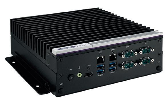
TINY ETHERNET MODULE
INDUSTRIAL MICROPROCESSORS
STMicroelectronics has released the STM32MP2 industrial microprocessors, from the second generation of its industrial microprocessors (MPUs), to drive progress in smart factories, smart health care, smart buildings and smart infrastructure.
The MPUs are designed to power the next generations of equipment such as industrial controllers and machine-vision systems, scanners, medical wearables, data aggregators, network gateways, smart appliances, and industrial and domestic robots.
Designed for demanding and time-sensitive workloads, AI inferencing and communication, the MPUs are built to withstand up to 10 years of continuous operation.
The new microprocessors leverage ST’s proprietary secure hardware, anti-tamper controls, protected firmware and secure provisioning, working with Arm’s TrustZone architecture, to keep sensitive data and keys secret. Certified to SESIP Level 3, the MPUs can meet forthcoming cyber-protection requirements in key territories worldwide. These include the US CyberTrust mark and stipulations in the EU’s Radio Equipment Directive that are due to become mandatory in 2025.
The first STM32MP2 MPUs will enter volume production in June 2024.
STMicroelectronics Pty Ltd www.st.com
ICP Electronics Australia has launched the ICP DAS tET-AD2, designed to enhance the efficiency of industrial processes. This tiny Ethernet module features isolated 2-channel analog inputs, offering versatility in monitoring and control tasks within a wide array of industrial applications. It comes equipped with a web server for straightforward configuration, thereby reducing set-up time and complexity.
Supporting a range of communication protocols including Modbus TCP/UDP, MQTT and SNMP V2c, the tiny Ethernet module enables integration into existing networks, facilitating real-time data exchange and analysis. Its I/O pair connection feature, enabling push and pull functionality, further enhances its adaptability in complex automation set-ups.
The module is designed to endure challenging industrial environments, featuring dual-watchdog support and the capability for firmware updates via Ethernet. With built-in I/O that includes 2-channel single-ended inputs for both voltage and current, the module enables flexible data acquisition.
Adjustable sampling rates, available in fast or normal modes, cater to varied application requirements, facilitating performance in diverse operational contexts such as industrial automation, machinery, building automation, food and beverage systems, semiconductor fabrication and control systems. Its robust design also includes 4 kV ESD protection and 3000 VDC intra-module isolation.
ICP Electronics Australia Pty Ltd www.icp-australia.com.au
34 MAY/JUNE 2024 WWW.ELECTRONICSONLINE.NET.AU

ETHERNET I/O MODULE
ICP Electronics Australia has launched the ICP DAS ET-2217CI-4, an Ethernet I/O module that integrates four channels of analog input with channel-to-channel isolation. This module is designed to enhance the precision of voltage and current monitoring while providing protection against overvoltages and overcurrents, thereby safeguarding critical industrial processes. With its versatile input range configuration, the module caters to diverse measurement needs, accommodating ±1 V, ±2.5 V, ±5 V, ±10 V, 0 to 20 mA, 4 to 20 mA and ±20 mA inputs, each configurable for specific requirements.
The module also features an adjustable sampling rate, offering both a fast mode at 200 Hz and a standard mode at 10 Hz/channel, enabling the monitoring and analysis of voltage and current data. This module supports essential protocols such as Modbus TCP/UDP and MQTT for integration into IoT ecosystems. The inclusion of a 2-port Ethernet switch with LAN bypass facilitates daisy-chain wiring, simplifying network configurations and enhancing connectivity.
Moreover, the ET-2217CI-4 features a built-in web server for hassle-free configuration, while an I/O Pair Connection facilitates efficient data synchronisation. Its capacity to log up to 480,000 records/channel, complete with time stamps, offers an extensive data analysis tool. Certified with CE, UKCA, FCC, RoHS and WEEE, this module meets a range of standards, for safety in industrial environments. Whether it’s for manufacturing, energy management or smart automation, the ET2217CI-4 Ethernet I/O Module is engineered to deliver integration ease, marking a step forward in industrial connectivity and monitoring solutions.
ICP Electronics Australia Pty Ltd www.icp-australia.com.au

SMA COAXIAL CONNECTORS
Richardson RFPD, Inc. has launched a range of lead-free radio frequency SMA connectors from HUBER+SUHNER. This new product family leverages HUBER+SUHNER’s SMA interface in a lead-free solution for connectors that are designed to deliver the same levels of electrical performance and mechanical properties as conventional connectors. The lead-free SMA connectors feature a broadband frequency range of up to 18 GHz and offer enhanced return loss and high mechanical strength. They are also inter-mateable with PC3.5 adapters and SK connectors. The SMA connectors are suitable for communications, defence, aviation, test and measurement, and a range of industrial applications.
Richardson RFPD www.richardsonrfpd.com
EMBEDDED MODULE
Axiomtek has launched the CEM320, an addition to its line-up of COM Express Type 10 modules. This embedded module features an on-board Intel Atom x6000E/RE series or Intel Celeron N/J processor (codenamed Elkhart Lake) with integrated Intel UHD graphics and high-speed interfaces. It comes equipped with integrated on-board 16 GB LPDDR4 memory, along with on-board eMMC 5.1 storage. The module also features enhanced graphics performance and is suitable for a range of applications, including medical imaging, industrial control, transportation surveillance systems, portable equipment and automation.
Equipped with Intel integrated UHD graphics, this module supports dual simultaneous displays via DDI port supporting HDMI/DVI/DisplayPort and single-channel 18/24-bit LVDS. Additionally, the module features a 2.5G LAN port with Wakeon-LAN and PXE Boot ROM enabled, as well as eMMC storage with up to 64 GB memory, for fast data transmission with low latency in automation applications or handheld devices in specific fields. The module also offers a variety of I/O options, including four PCIe x1 Gen3 lances, two USB 3.2
Gen2 ports, eight USB 2.0 ports, one 2.5G LAN port with Intel Ethernet Controller I226-LM, two SATA 3.0 ports, HD Codec audio, one DDI, one LVDS (eDP optional), one LPC, one SPI, two serial TX/RX, one I2C, and 4-channel GPIO. These features provide customers with a range of options to address diverse digital connectivity challenges.
In addition to its flexible I/O expansion, the module is designed to support a wide voltage input range of +4.75 to +20 V, catering to the varying voltage input requirements of automotive or portable applications. It also offers extended operating temperature ranges of -20 to +70ºC or -40 to +85ºC with a system thermal solution to facilitate operation in harsh environments. The CEM320 module also supports a watchdog timer and TPM 2.0 for enhanced system security. Tekdis www.tekdis.com.au
36 MAY/JUNE 2024 WWW.ELECTRONICSONLINE.NET.AU
NAVIGATING REGULATORY LANDSCAPES: THE CRUCIAL ROLE OF PRODUCT COMPLIANCE FOLDERS IN THE AUSTRALIAN AND NEW ZEALAND MARKETS

In the dynamic landscape of electrical, radiocommunication and telecommunication equipment, adherence to regulatory standards stands as a cornerstone for both manufacturers and importers. Central to this commitment is the establishment and upkeep of a robust product compliance folder. This collaborative conversation with Comtest Group delves into the pivotal role such folders play in navigating the intricacies of the Australian and New Zealand markets, shedding light on their indispensable nature.
At the core of the imperative lies legal obligations. Compliance with regulatory standards transcends mere preference, constituting a binding legal mandate in Australia and New Zealand. Australia and New Zealand boast stringent regulations governing the safety, radiocommunications, electromagnetic energy, and electromagnetic compatibility of electrical and telecommunication equipment. Leveraging Comtest Group’s regulatory prowess, importers and manufacturers can adeptly manoeuvre these legal requisites, ensuring seamless alignment with all prescribed standards and regulations.
Market access stands as another compelling reason underpinning the necessity of product compliance folders. The Australian and New Zealand markets, characterised by our regulatory rigor, proscribe entry or withdrawal from shelves for non-compliant products. Comtest Group extends a suite of comprehensive compliance services encompassing testing, certifi cation, and documentation support, facilitating expedited market access. Through our collaborative efforts, importers and manufacturers stand poised to streamline the certification and approval process, thereby garnering a competitive edge within these markets.
Consumer safety emerges as a paramount concern for regulatory authorities across Australia and New Zealand. Comtest Group’s meticulous testing protocols and compliance acumen serve to identify and mitigate potential safety hazards inherent in electrical, radiocommunication and telecommunication equipment. By forging partnerships with us, importers and manufacturers can showcase their unwavering commitment to consumer safety while concurrently adhering to regulatory benchmarks.
Mitigation of risks constitutes yet another compelling rationale for prioritising compliance. Non-compliance entails a gamut of
ramifications spanning legal repercussions, tarnished reputations, and financial losses. Comtest Group adopts a proactive stance towards compliance management, empowering importers and manufacturers to mitigate these risks through the provision of readily available and up-to-date documentation. Our holistic suite of compliance services instils a sense of reassurance, enabling businesses to channel their energies towards innovation and growth without the spectre of compliance-related anxieties.
In a landscape marked by regulatory dynamism, staying abreast of updates assumes paramount importance. Regulatory standards and requirements undergo constant change, necessitating diligent monitoring and subsequent updates to compliance documentation. Comtest Group’s skilled team of experts remains vigilantly attuned to regulatory developments, ensuring prompt updates to compliance folders reflective of any alterations. By forging alliances with us, importers and manufacturers can maintain ongoing compliance with regulatory benchmarks, thereby sidestepping potential penalties and fines.
In summation, the establishment and ongoing maintenance of a product compliance folder emerge as non-negotiable imperatives for importers and manufacturers of electrical, radiocommunication and telecommunication equipment endeavouring to penetrate or continue their presence within the Australian and New Zealand markets. Armed with Comtest Group’s comprehensive compliance services, businesses can navigate regulatory exigencies with assurance, thereby ensuring unfettered market access, consumer safety, and risk mitigation. For more information, visit our website or contact us today to embark on the journey towards compliance excellence within the Australian and New Zealand markets.


Comtest@comtest.com.au

+61 3 9645 5933 www.comtestgroup.com.au


Comtest Group www.comtestgroup.com.au

WWW.ELECTRONICSONLINE.NET.AU MAY/JUN 2024 37 SPONSORED CONTENT
iStock.com/AF-studio
EMBEDDED FANLESS PC
Backplane Systems Technology has launched the Sintrones VBOX3630RP-M12X embedded fanless PC, designed for the needs of fleet management and in-vehicle applications. Powered by the Intel 11th Gen Core i7-1185G7E CPU, this onboard computer enables advanced vehicle monitoring, management and digital signage capabilities.
With support for dual 5G/LTE, GPS, Wi-Fi/Bluetooth and CAN bus, the embedded fanless PC is designed to provide constant connectivity and real-time data transmission for efficient fleet operations. Its isolated DC input, ranging from 24 to 110 VDC with power management, caters to the power requirements of rolling stock, highlighting its suitability for a range of vehicular environments.
The computer’s connectivity is enhanced by its 1x 2.5GbE and 3x GbE LAN ports, all equipped with M12 connectors to facilitate network connections even in harsh conditions. Additionally, it supports up to four independent displays through 2x HDMI, 1x DP and 1x DVI-D ports, enabling versatile multimedia applications.
Certified with E-Mark & EN50155, the VBOX-3630RP-M12X embedded fanless PC meets industry standards for automotive and railway applications. Its optional backup battery kit makes it suitable for managing fleets, in-vehicle signage and mobile DVR systems. Designed to operate in extreme weather and operating conditions, it is also suitable for vehicles like snowploughs, trucks, buses, taxis and forklifts. Backplane Systems Technology Pty Ltd www.backplane.com.au

ENCLOSURE
SERIAL COMMUNICATION BOARD
ICP Electronics Australia has launched the ICP DAS PCIeS114 serial communication board. Designed to slot into PCI Express x1 interfaces, this compact card offers four RS-232 ports to facilitate a range of serial communication tasks. Each port is backed by a 256-byte hardware FIFO, to enable smooth and efficient data transfer at speeds up to 921600 bps, even in full-duplex modes.
The card’s design includes on-board photo couplers for the ‘i’ version, which provide electrical isolation between the serial ports and the host computer. This feature helps minimise the risks associated with ground loops, common mode voltages and voltage spikes, thereby safeguarding both the PCIe-S114 and connected devices against electrical interference and over-voltage conditions.
Additionally, the presence of on-board ESD protection components further enhances the safety of sensitive circuitry, making the serial communication board suitable for applications in harsh industrial environments. Supported by drivers for a range of operating systems, the PCIe-S114 is versatile and designed to meet the demands of industrial machinery, building automation, restaurant appliances, laboratory equipment and more.
ICP Electronics Australia Pty Ltd www.icp-australia.com.au
ROLEC OKW has added a closed-front flat version to its RAILTEC B DIN rail enclosures range that is designed to provide greater protection for electronics.
RAILTEC B is suitable for a range of applications including automation, building and safety technology, HVAC, communications and measurement. The enclosure is designed to save space; its closed front also has a large area for displays, operating elements and interfaces.
The enclosure can also be mounted on TH35 DIN rails or directly on walls. The enclosure is also fully insulated and protected in accordance with VBG 4 and IEC 529/DIN VDE 0470-1. The upper parts of the enclosure are moulded from flame-retardant (UL 94 V-0) PC in light grey (RAL 7035) while the lower parts are black PPO (UL 94 V-0).
The new closed-front flat version is available in four module widths: 2, 4, 6 and 9 with sizes ranging from 35 x 89.6 x 31.25 mm to 157.5 x 89.6 x 31.25 mm.
Accessories for the closed-front flat version include a wall suspension element and screws for fitting PCBs and mounting plates. Accessories for other versions of the RAILTEC B also include terminal blocks, plug headers, lids, front panels, terminal guards and partition plates. OKW can supply RAILTEC B fully customised. Services include machining, lacquering, printing, laser marking, decor foils and installation/assembly of accessories.
ROLEC OKW Australia New Zealand P/L www.okw.com.au
38 MAY/JUNE 2024 WWW.ELECTRONICSONLINE.NET.AU
COMPACT CHIPS COULD ENHANCE NAVIGATION AND COMMUNICATION

The National Institute of Standards and Technology (NIST) and its collaborators have delivered a small but mighty advancement in timing technology: compact chips that seamlessly convert light into microwaves.
These chips could improve GPS, the quality of phone and internet connections, the accuracy of radar and sensing systems, and other technologies that rely on high-precision timing and communication.
This technology reduces something known as timing jitter, which is small, random changes in the timing of microwave signals. Similar to when a musician is trying to keep a steady beat in music, the timing of these signals can sometimes waver a bit. The researchers have reduced these timing wavers to a very small fraction of a second — 15 femtoseconds to be exact, a big improvement over traditional microwave sources — making the signals
much more stable and precise in ways that could increase radar sensitivity, the accuracy of analog-to-digital converters and the clarity of astronomical images captured by groups of telescopes. The team’s results were published in Nature
Shining a light on microwaves
What sets this demonstration apart is the compact design of the components that produce these signals. For the first time, researchers have taken what was once a tabletop-size system and shrunken much of it into a compact chip, about the same size as a digital camera memory card. Reducing timing jitter on a small scale reduces
power usage and makes it more usable in everyday devices.
Right now, several of the components for this technology are located outside of the chip, as researchers test their effectiveness. The ultimate goal of this project is to integrate all the different parts, such as lasers, modulators, detectors and optical amplifiers, onto a single chip.
By integrating all the components onto a single chip, the team could reduce both the size and power consumption of the system. This means it could be easily incorporated into small devices without requiring lots of energy and specialised training. >
WWW.ELECTRONICSONLINE.NET.AU MAY/JUN 2024 39
TIMING TECHNOLOGY iStock.com/Chor muang
NIST researchers test a chip for converting light into microwave signals. Pictured is the chip,
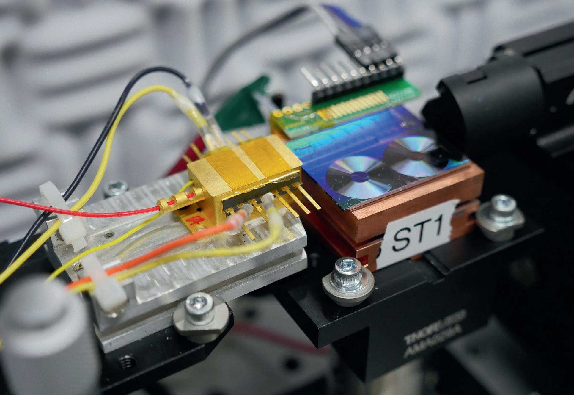
“The current technology takes several labs and many PhDs to make microwave signals happen,” said Frank Quinlan, NIST physical scientist. “A lot of what this research is about is how we utilise the advantages of optical signals by shrinking the size of components and making everything more accessible.”
To accomplish this, researchers use a semiconductor laser, which acts as a very steady flashlight. They direct the light from the laser into a tiny mirror box called a reference cavity, which is like a miniature room where light bounces around. Inside this cavity, some light frequencies are matched to the size of the cavity so that the peaks and valleys of the light waves fit perfectly between the walls. This causes the light to build up power in those frequencies, which is used to keep the laser’s frequency stable. The stable light is then converted into microwaves using a device called a frequency comb, which changes high-frequency light into lower-pitched microwave signals. These precise microwaves are crucial for technologies like navigation systems, communication networks and radar because they provide accurate timing and synchronisation.
“The goal is to make all these parts work together effectively on a single platform, which would greatly reduce the loss of signals and remove the need for extra technology,” Quinlan said. “Phase one of this project was to show that all these individual pieces work together. Phase two is putting them together on the chip.”
WHAT SETS THIS DEMONSTRATION APART IS THE COMPACT DESIGN OF THE COMPONENTS THAT PRODUCE THESE SIGNALS.
In navigation systems such as GPS, the precise timing of signals is essential for determining location. In communication networks, such as mobile phone and internet systems, accurate timing and synchronisation of multiple signals ensure that data is transmitted and received correctly.
For example, synchronising signals is important for busy cell networks to handle multiple phone calls. This precise alignment of signals in time enables the cell network to organise and manage the transmission and reception of data from multiple devices, like your cellphone. This ensures that multiple phone calls can be carried over the network simultaneously without experiencing significant delays or drops.
In radar, which is used for detecting objects like aeroplanes and weather patterns, precise timing is crucial for accurately measuring how long it takes for signals to bounce back.
“There are all sorts of applications for this technology. For instance, astronomers who are imaging distant astronomical objects, like black holes, need really low-noise signals and clock synchronisation,” Quinlan said. “And this project helps get those low
noise signals out of the lab, and into the hands of radar technicians, of astronomers, of environmental scientists, of all these different fields, to increase their sensitivity and ability to measure new things.”
Working together towards a shared goal
Creating this type of technological advancement is not done alone. Researchers from the University of Colorado Boulder, the NASA Jet Propulsion Laboratory, California Institute of Technology, the University of California Santa Barbara, the University of Virginia and Yale University came together to accomplish this shared goal: to revolutionise how we harness light and microwaves for practical applications.
“I like to compare our research to a construction project. There’s a lot of moving parts, and you need to make sure everyone is coordinated so the plumber and electrician are showing up at the right time in the project,” Quinlan said. “We all work together really well to keep things moving forward.”
This collaborative effort underscores the importance of interdisciplinary research in driving technological progress, Quinlan said.
40 MAY/JUNE 2024 WWW.ELECTRONICSONLINE.NET.AU
TIMING TECHNOLOGY
which is the fluorescent panel that looks like two tiny vinyl records. The gold box to the left of the chip is the semiconductor laser that emits light to the chip.
K.Palubick/NIST

EMBRACING THE FUTURE: THE IMPERATIVE FOR DIGITISATION AND CONDITION MONITORING IN INDUSTRIAL AND MOBILE EQUIPMENT
In an era marked by rapid technological advancements, the industrial and mobile equipment sector stands at the precipice of a transformative shift towards digitisation and condition monitoring. This evolution is not merely a technological trend; it is a necessity dictated by the escalating complexity of integrated systems, the demand for heightened efficiency, and the imperative to future-proof against the relentless march of automation.
Complexity of Integrated Systems:
As industrial and mobile equipment become more sophisticated, traditional methods of maintenance by less qualified technicians are proving insufficient. Integrated systems are becoming intricate ecosystems, where a single fault can have cascading effects. Digitisation and condition monitoring offer a holistic approach, enabling the tracking and analysis of every component in realtime, ensuring that only qualified personnel armed with actionable insights can effectively address emerging issues.
Time and Energy Efficiency in Predictive Maintenance:
The traditional reactive maintenance model is becoming obsolete in the face of digitisation. With condition monitoring, faults can be predicted and analysed remotely, reducing downtime significantly. This shift from reactive to predictive maintenance not only enhances operational efficiency but also ensures that service interventions occur precisely when needed, minimising the impact on productivity.
One of the compelling advantages of digitisation and condition monitoring is the reduction in carbon emissions, through efficiency and reliability gains. As industries strive to meet stringent sustainability goals and minimise their environmental footprint, the optimisation of equipment performance becomes paramount. By leveraging real-time data and analytics, businesses can identify and rectify inefficiencies promptly, resulting in more energy-efficient operations. This not only aligns with global efforts towards sustainable practices but also brings about substantial cost savings, creating a win-win situation for both the environment and the bottom line.
Future-Proofing for Automation:
As automation continues to reshape industries, embracing digitisation and condition monitoring is a strategic imperative. These technologies provide a foundation for seamless integration with emerging automated systems, allowing for a smooth transition into an increasingly automated future. By investing in these
advancements now, industries can position themselves at the forefront of technological innovation and maintain a competitive edge.
Reduced Service Costs:
One of the most compelling arguments for digitisation and condition monitoring is the significant reduction in service costs. Traditional maintenance models often lead to unnecessary downtime and expenditures. With real-time monitoring and predictive analytics, equipment can communicate service needs and required parts in advance, allowing for precise planning and cost-effective maintenance interventions. This not only reduces operational costs but also enhances overall budgetary predictability. As these systems become more intricate, the demand for highly qualified technicians capable of troubleshooting and maintaining them is escalating. However, the reality of current large skills shortages poses a significant challenge.
Overcoming Resistance to Technology:
Acknowledging that resistance to new technology is a natural human instinct, it is essential to address these concerns proactively. Providing comprehensive training programs, showcasing tangible benefits through pilot projects, and emphasising the user-friendly nature of these solutions can alleviate fears and demonstrate that embracing digitisation is not just a leap into the unknown but a calculated step towards a more efficient and sustainable future.
Conclusion:
In conclusion, the imperative for digitisation and condition monitoring in industrial and mobile equipment is not merely a response to current needs; it is an investment in the future. By overcoming resistance through education and showcasing the tangible benefits, industries can position themselves to thrive in an era where adaptability and efficiency are the cornerstones of success. The shift towards digitisation is not a choice but a strategic necessity, ensuring a competitive edge and sustainability in an ever-evolving industrial landscape.
HYDAC have invested heavily in digitisation, carbon minimisation technology, advanced skills training courses and more. We are well placed to be the partner to assist Australian industry achieve digital transformation and long-term cost reductions, via efficiency and reliability gains.

WWW.ELECTRONICSONLINE.NET.AU MAY/JUN 2024 41 HYDAC
International www.hydac.com.au
SPONSORED CONTENT
RECYCLABLE CIRCUIT BOARD TURNS TO JELLY FOR DISASSEMBLY
Stefan Milne

In a 30 mL glass beaker filled with clear liquid, tweezers remove a piece of vitrimer plastic. A square sheet of glass fibres sits in the background, leaning against the side of the beaker.
42 MAY/JUNE 2024 WWW.ELECTRONICSONLINE.NET.AU
Mark Stone/University of Washington.
A recent United Nations report found that the world generated 137 billion pounds of electronic waste in 2022, an 82% increase from 2010. Yet less than a quarter of 2022’s e-waste was recycled. While many things impede a sustainable afterlife for electronics, one is that we don’t have systems at scale to recycle the printed circuit boards (PCBs) found in nearly all electronic devices.
PCBs — which house and interconnect chips, transistors and other components — typically consist of layers of thin glass fibre sheets coated in hard plastic and laminated together with copper. That plastic can’t easily be separated from the glass, so PCBs often pile up in landfills, where their chemicals can seep into the environment. Or they’re burned to extract their electronics’ valuable metals like gold and copper. This burning, often undertaken in developing nations, is wasteful and can be toxic — especially for those doing the work without proper protections.
A team led by researchers at the University of Washington developed a new PCB that performs on par with traditional materials and can be recycled repeatedly with negligible material loss. Researchers used a solvent that transforms a type of vitrimer — a cutting-edge class of sustainable polymers — to a jellylike substance without damaging it, allowing the solid components to be plucked out for reuse or recycling.
The vitrimer jelly can then be repeatedly used to make new, high-quality PCBs, unlike conventional plastics that degrade significantly with each recycling. With these “vPCBs” (vitrimer printed circuit boards), researchers
recovered 98% of the vitrimer and 100% of the glass fibre, as well as 91% of the solvent used for recycling.
The researchers have published their findings in Nature Sustainability
“PCBs make up a pretty large fraction of the mass and volume of electronic waste,” said co-senior author Vikram Iyer, a UW assistant professor in the Paul G. Allen School of Computer Science & Engineering. “They’re constructed to be fireproof and chemical-proof, which is great in terms of making them very robust. But that also makes them basically impossible to recycle. Here, we created a new material formulation that has the electrical properties comparable to conventional PCBs as well as a process to recycle them repeatedly.”
Vitrimers are a class of polymers first developed in 2015. When exposed to certain conditions, such as heat above a specific temperature, their molecules can rearrange and form new bonds. This makes them both ‘healable’ (a bent PCB could be straightened, for instance) and highly recyclable.
“On a molecular level, polymers are kind of like spaghetti noodles, which wrap and get compacted,” said co-senior author Aniruddh Vashisth, a UW assistant professor in the

mechanical engineering department. “But vitrimers are distinct because the molecules that make up each noodle can unlink and relink. It’s almost like each piece of spaghetti is made of small Legos.”
The team’s process to create the vPCB deviated only slightly from those used for PCBs. Conventionally, semi-cured PCB layers are held in cool, dry conditions where they have a limited shelf life before they’re laminated in a heat press. Because vitrimers can form new bonds, researchers laminated fully cured vPCB layers. The researchers found that to recycle the vPCBs they could immerse the material in an organic solvent that has a relatively low boiling point. This swelled the vPCB’s plastic without damaging the glass sheets and electronic components, letting the researchers extract these for reuse.
This process allows for several paths to more sustainable, circular PCB lifecycles. Damaged circuit boards, such as those with cracks or warping, can in some cases be repaired. If they aren’t repaired, they can be separated from their electronic components. Those components can then be recycled or reused, while the vitrimer and glass fibres can get recycled into new vPCBs.
The team tested its vPCB for strength and electrical properties, and found that it performed comparable to the most common PCB material (FR-4). Vashisth and co-author Bichlien H Nguyen, a principal researcher at Microsoft Research and an affiliate assistant professor in the Allen School, are now using artificial intelligence to explore new vitrimer formulations for different uses.
Producing vPCBs wouldn’t entail major changes to manufacturing processes.
“The nice thing is that a lot of industries — such as aerospace, automotive and even electronics — already have processing set up for the sorts of two-part epoxies that we use here,” said lead author Zhihan Zhang, a UW doctoral student in the Allen School.
The team analysed the environmental impact and found recycled vPCBs could entail a 48% reduction in global warming potential and an 81% reduction in carcinogenic emissions compared to traditional PCBs. While this work presents a technology solution, the team notes that a significant hurdle to recycling vPCBs at scale would be creating systems and incentives to gather e-waste so it can be recycled.
“For real implementation of these systems, there needs to be cost parity and strong governmental regulations in place,” Nguyen said. “Moving forward, we need to design and optimise materials with sustainability metrics as a first principle.”
WWW.ELECTRONICSONLINE.NET.AU MAY/JUN 2024 43
A small brown circuit board sits on a grey background. Surrounding it are a small copper plate, a sheet of clear vitrimer plastic, computer chips, sheets of glass fibres in a crosshatch pattern and small chunks of vitrimer plastic that’s been removed from a chip.
SUSTAINABILITY
Mark Stone/University of Washington.

REMOTE ENGINEERING HARDWARE SYSTEM
DigiKey has released the LabsLand Prism4, a modular structure for building interactive real-time, remote hardware systems more efficiently. The Prism4’s design supports remote hardware systems with cameras, modular lights and evaluation boards. The platform also includes a set of Phase Dock workbench bases where devices can be attached using clicks and slides.
Each Prism4 hosts specific ready-to-ship Prism4 hardware systems that are available for different technologies, including field programmable gate arrays (FPGAs), select microprocessors and microcontrollers. In addition, the Prism4’s system design supports the creation of remote laboratories for other fields, allowing for a variety of uses, such as remote education and training using real equipment.
With the development and release of the Prism4 through DigiKey, engineers, designers and suppliers have access to a remote engineering platform for new product demonstration, evaluation, product testing and design, allowing engineers to try out hardware before purchasing. Software engineers can also use the platform to learn and develop code and program remote targets using actual hardware instead of simulators. The Prism4 hardware system enables users to control and interact with the target platforms while providing video feedback demonstrating outcomes and results in real time.
DigiKey engaged with a design integration service provider to jump-start the design process and then collaborated with Phase Dock and LabsLand on the final product.
Digi-Key Electronics www.digikey.com
EMC_ad_2019.pdf 1 10/05/2023 10:32:41 AM


WIRELESS MICROCONTROLLERS
STMicroelectronics has launched the STM32WBA5 series of short-range wireless microcontrollers. These innovative, all-in-one components enable wearables and smart objects, including smart home devices, health monitors and smart appliances, to become more miniaturised and easy to use.
The series is compatible with the development tools and software packs of the STM32 microcontroller development ecosystem, thereby simplifying the process of migrating existing products designed for wired connections.
The microcontroller can communicate using multiple wireless standards concurrently, including low-energy Bluetooth LE 5.4, Zigbee, Thread and Matter (Thread RCP). The matter border router is also a match with the STM32WBA5 for this new open-source connectivity standard for smart home and IoT (Internet of Things) devices. In this way, the wireless microcontroller supports user experiences while simplifying hardware and software engineers’ development journey.
With this new generation, ST has also introduced support for the Bluetooth LE Audio specifications that enable innovative new products for enhanced listening and hearing experiences. These include the Bluetooth Auracast feature.
The STM32WBA series has also achieved the SESIP (Security Evaluation Standard for IoT Platforms) Level 3 security certification. With this, smart devices containing STM32WBA microcontrollers are ready to satisfy the US Cyber Trust Mark and EU Radio Equipment Directive (RED) regulations due to become mandatory in 2025.
STMicroelectronics Pty Ltd www.st.com
44 MAY/JUNE 2024 WWW.ELECTRONICSONLINE.NET.AU
Accredited testing and global product approvals since 1992
Bayswater
HIDDEN SEMICONDUCTOR ACTIVITY SPOTTED BY RESEARCHERS
Jamie Oberdick, Penn State News

Using advanced imaging techniques, an international team led by Penn State researchers found that the material that a semiconductor chip device is built on, called the substrate, responds to changes in electricity much like the semiconductor on top of it.
The researchers worked with the semiconductor material, vanadium dioxide, which they said shows great potential as an electronic switch. They also studied how vanadium dioxide interacts with the substrate material titanium dioxide and said they were surprised to discover that there seems to be an active layer in the substrate that behaves similarly to the semiconductor material on top of it when the semiconductor switches between an insulator — not letting electricity flow — and a metal — letting electricity flow. The revelation that substrates can play an active role in semiconductor processes is significant for designing future materials and devices, said study lead Venkatraman Gopalan, professor of materials science and engineering and of physics at Penn State.
New research suggests that materials commonly overlooked in computer chip design actually play an important role in information processing, a discovery which could lead to faster and more efficient electronics.
“New ideas are needed for smaller and faster electronics in order to keep up with Moore’s law,” said Gopalan, the corresponding author of the study in Advanced Materials “One idea being pursued is materials, such as vanadium dioxide, that can switch between metal — the one state — and insulator — the zero state — states in a trillionth of a second. This is known as undergoing metal-insulator transitions.”
The potential of vanadium dioxide as a metal-to-insulator transistor is well documented and the material is considered promising for semiconductor technology due to its low energy consumption, Gopalan said. However, the material’s properties are still not fully understood, and until now, it has usually been observed in isolation rather than while functioning in a real device.
Vanadium dioxide has strongly correlated electronic effects, meaning the repulsion between electrons interferes with the device, so cannot be ignored as is currently done in silicon-based electronics. This characteristic can result in materials with novel functionalities such as high-temperature superconductivity and enhanced magnetic properties.
“The underlying physics of this material is less understood, and its performance in a device geometry is even lesser understood,” Gopalan said. “If we can make them work, there will be a renaissance in electronics. In particular, neuromorphic computing — where computer systems that take inspiration from the brains of living systems with neurons — could seriously benefit by using such devices.”
WWW.ELECTRONICSONLINE.NET.AU MAY/JUN 2024 45
MATERIALS RESEARCH
>
iStock.com/koto_feja
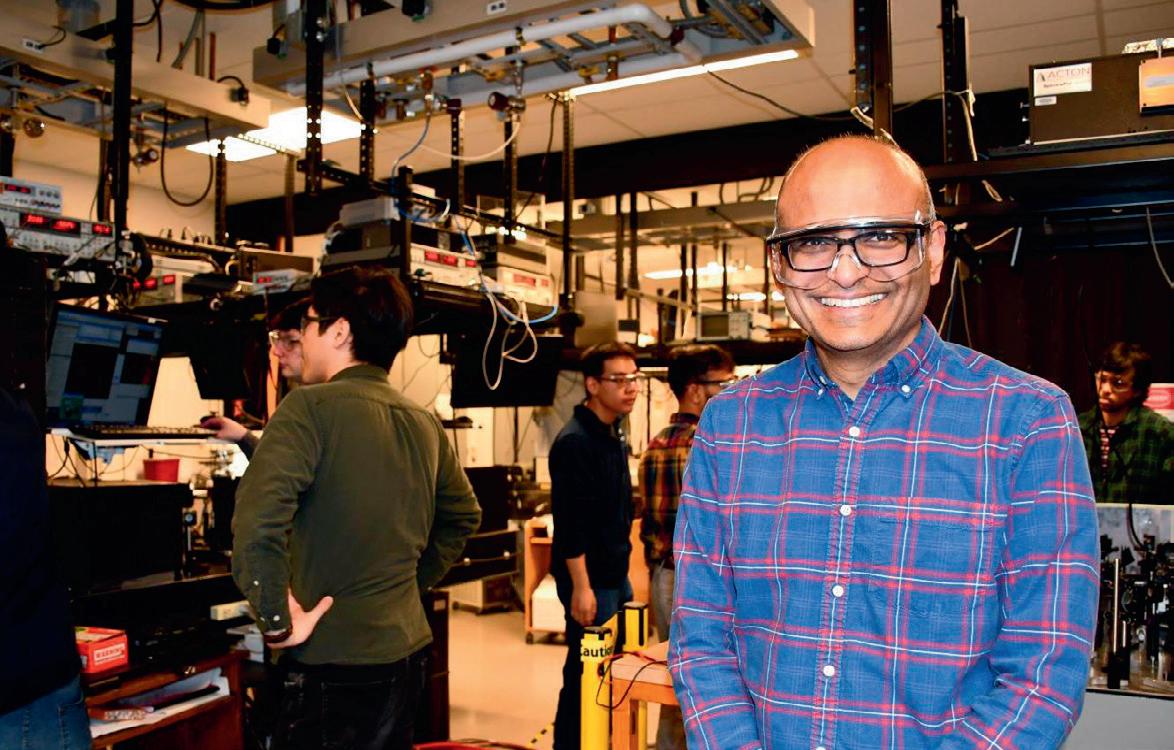
The team investigated vanadium dioxide in a device rather than in isolation, applying a voltage to it to make it switch from an insulating to a conducting state. They used the Advanced Photon Source (APS) at Argonne National Laboratory, which uses powerful X-ray beams to study the behaviour and structure of materials on the atomic level. When mapping the spatial and temporal response of the material to the switching event, the researchers observed unexpected changes to the structure of the material and substrate.
“What we found was that as the vanadium dioxide film changes to a metal, the whole film channel bulges, which is very surprising,” Gopalan said. “Normally it is supposed to shrink. So clearly something else was going on in the film geometry that was missed before.”
The APS X-ray penetrated through the vanadium dioxide film and into the titanium dioxide (TiO2) substrate — which is normally considered an electrically and mechanically passive material — that the thin film was grown on.
“We found to our great surprise that this substrate is very much active, jiving and responding in completely surprising ways as the film switches from an insulator to a metal and back, when the electrical pulses arrive,” Gopalan said. “This is like watching the tail wagging the dog, which stumped us for a long while. This surprising and previously overlooked observation completely changes how we need to view this technology.”
To understand these findings, the theory and simulation effort — led by Long-Qing Chen, Hamer Professor of Materials Science
and Engineering, professor of engineering science and mechanics and of mathematics at Penn State — developed a theoretical framework to explain the entire process of the film and the substrate bulging instead of shrinking. When their model incorporated naturally occurring missing oxygen atoms in this material of two types, charged and uncharged, the experimental results could be satisfactorily explained.
“These neutral oxygen vacancies hold a charge of two electrons, which they can release when the material switches from an insulator to a metal,” Gopalan said. “The oxygen vacancy left behind is now charged and swells up, leading to the observed surprising swelling in the device. This can also happen in the substrate. All of these physical processes are beautifully captured in the phase-field theory and modelling performed in this work for the first time by the postdoc Yin Shi in Professor Chen’s group.”
Gopalan credited the multidisciplinary team’s combined expertise in material growth, synthesis, structure analysis and synchrotron beamline operation with the new understanding. Using a collaborative approach led by Greg Stone, a physical scientist with the U.S. Army and the lead experimental author, and Yin Chi, postdoctoral scholar at Penn State and the lead theory author, the researchers disentangled the material’s responses and observed them individually using phase field simulations, a simulation that helps scientists understand material changes over time by depicting various states of matter in a virtual setting.
“By bringing these experts together and pooling our understanding of the problem,
THE REVELATION THAT SUBSTRATES CAN PLAY AN ACTIVE ROLE IN SEMICONDUCTOR PROCESSES IS SIGNIFICANT FOR DESIGNING FUTURE MATERIALS AND DEVICES.
we were able to go far beyond our individual scope of expertise and discover something new,” said Roman Engel-Herbert, Director of the Paul Drude Institute of Solid State Electronics in Berlin, Germany, and coauthor of the study whose group grew these films along with Darrell Schlom’s group at Cornell University. “Recognising the potential of functional materials necessitates an appreciation of their broader context, just as complex scientific challenges can only be solved through widening our individual perspectives.”
The collaboration enabled both a significant amount of progress to happen in a short period of time and work to be done in a shorter period of time, and brought in a variety of perspectives from multiple disciplines.
The responses themselves require further investigation, researchers said, but they believe that understanding them will assist in identifying previously unknown capabilities of vanadium dioxide, including potential yet-to-be-discovered phenomena in the TiO2 substrate that was considered passive before this study. The study itself unfolded over 10 years, Gopalan noted, including validating the results.
“This is what it takes to go from interesting science to a working device you can hold in the palm of your hand,” Gopalan said. “Experiments and theory are complex and require large-scale collaborative teams working closely together over an extended period of time to solve difficult problems that could have a large impact. We hope and expect that this will accelerate the progress towards a new generation of electronic devices.”
46 MAY/JUNE 2024 WWW.ELECTRONICSONLINE.NET.AU
Venkatraman Gopalan, professor of materials science and engineering and of physics, in his optical lab.
MATERIALS RESEARCH
Seana Wood/Penn
State Materials Research
Institute.
CAMERA FRAME GRABBER CARD
Backplane Systems Technology is has launched the Neousys PCIe-GL26, an AI-enabled 6-port GMSL2 camera frame grabber card designed to enhance automotive vision systems and autonomous vehicle technologies. Equipped with six GMSL2 FAKRA Z inputs, it supports automotive GMSL2 cameras, making it a versatile solution for integrating advanced vision capabilities into automotive applications.
This industrial-grade frame grabber is a turnkey solution that includes pre-installed drivers for selected GMSL2 cameras, along with video streaming sample codes, simplifying the integration process. It features the NVIDIA Jetson Xavier NX, bundled with JetPack 4.6.1, to deliver 21 TOPS of AI performance. This enables the device to handle up to 22 streams of 1080p@30FPS video encoding simultaneously.
The card features a dual Gen3 PCI Express interface offering a total bandwidth of 10 Gbps, a GPS PPS input for frame synchronisation and connectivity options including isolated CAN 2.0 and RS232 ports. The camera frame grabber card is designed to operate in a range of temperatures, from -25 to 60°C, with adequate airflow.
Suitable for use in autonomous vehicles and computer vision applications in varying outdoor lighting conditions, the PCIe-GL26 enables high-quality image capture with minimal latency. Its ability to support up to 24x GMSL2 camera streams across multiple cards in a single system, along with its synchronisation features, makes it suitable for advanced ADAS or autonomous driving systems seeking AI-driven sensor fusion.
Backplane Systems Technology Pty Ltd www.backplane.com.au
RGB LEDs
Würth Elektronik now offers WLICLED, a series of RGB LEDs with integrated controllers (IC). The components, controllable as pixels, combine a red, green and blue LED with a programmable controller IC. The intelligent LEDs, available in four designs, are individually controllable in their pixel colour, with brightness levels from 0 to 100%.
Over 16 million different colour and brightness levels can be set with the new RGB LEDs. They are compatible with open source libraries such as FastLED. As fewer components (such as series resistors) are required, display solutions with intelligent LEDs are not only quicker to implement, they are more compact than solutions with separate LEDs. Applications for the components include signal control systems, full-colour matrix displays, audio and gaming systems, indoor lighting and displays on e-mobility charging stations. The following designs are now available: 2020 Chip LED compact, 3210 Chip LED Side View, 2121 PLCC6 with bypass and 5050 PLCC4.
The intelligent LEDs feature an MSL3 moisture sensitivity level (rather than the commonly found MSL5a or MSL6), thereby reducing moisture sensitivity during assembly. Some of the components comply with protection class IPx7, so they can even be submerged for a short time without damage. The LED chipsets also feature gold coating on the Chip LED models and silver coating for PLCC models, which leads to better solderability. Available in 8-bit and 12-bit versions, the intelligent LEDs offer more options for PWM resolution. Photobiological test reports in accordance with EN 62471:2008 and IEC 62471:2006 are available for all models in the product group. This may be relevant if the intelligent LEDs are used in toys. The LEDs with integrated controllers can now be ordered from stock without a minimum order quantity. Developers can receive free samples.
Wurth Electronics Australia Pty www.we-online.com


WWW.ELECTRONICSONLINE.NET.AU MAY/JUN 2024 47
MOUSER ELECTRONICS LOOKS TO THE FUTURE AS IT CELEBRATES 60TH ANNIVERSARY

Mouser Electronics, Inc., a global distributor of electronic components and industrial automation parts, has marked its 60th year in business. The company began with a couple of employees working out of a garage in El Cajon, California and is now a global corporation with 4000 employees and 28 locations worldwide, including a new service centre in Melbourne, Australia. Much has changed in the electronics industry since 1964, but Mouser has remained dedicated to providing innovative technology to customers as quickly as possible. Along with its 28 locations, Mouser’s central hub is the company’s global headquarters and distribution centre on its 100-acre campus in Mansfield, Texas.
Below, Mark Burr-Lonnon, Mouser Electronics’ Senior Vice President of Global Service & EMEA and APAC Business, shares his insights into the current trends affecting the electronics industry.
2024 marks Mouser Electronics’ 60th year in business. What would you attribute to the company’s enduring success?
A lot of it is built around technology leadership. Certainly from our standpoint, we focus a lot on being a technology leader and taking new products to market for our key suppliers. That’s a big thing for us, we have a huge portfolio of parts and franchised parts, that’s probably 1300 franchises now — it’s almost hard to find one that we don’t have! That really drives what we do and at the back end of that is the inventory that we put into place.
We’ve got over $2 billion of inventory and that means if people need the inventory today or tomorrow or in three days’ time, depending on where they are in the world, then we typically have it for them. That’s the key thing that drives what we do. We’re very focused on not getting involved with the volume side of the business and the supply chain; it’s almost impossible to be a supply chain distributor and do what we do. I think we’ve got ourselves into a nice niche.
When you look at that type of niche, it’s easy to say that we’re never going to be huge by doing that, but with the way the electronics market is going to continue to grow in the foreseeable future — I mean, you can’t see anything having less electronics in it — so I think we’re in the right place and doing the right things.
What is your assessment of the worldwide market conditions for semiconductors and electronic components, and how do you think they will impact Mouser’s business development plans?
The worldwide market affects us hugely; it is the reason we went from $2 billion to $4 billion in two years. The market has a real bearing on how successful you can be. But you have to do the right things and be in the right place at the right time. If you look at it, 2021 and 2022 were phenomenal from our standpoint in the industry, they were good times. This year and last year it was okay, we see Q3 and Q4 beginning to be on the rise again. Next year I think we’ll be back to having a banner year, so I think the global market will see big changes in 2025 and we’ll be back on track for some serious growth.
What will be the biggest growth opportunities for Mouser Electronics in 2024?
It’s hard to say, because we’ve got over 850,000 customers and there is no sector that we’re not in, so it almost doesn’t matter what grows. If people ask us who we are and what we do, sometimes we say that we’re a marketing company; we view that the key to our success is adding a new warehouse, adding more inventory and the marketing team doing more to bring people to the inventory — whether it’s through Google or in-house marketing.
Some people ask us a question, we say we’re a marketing company who happens to sell components — which is sort of
48 MAY/JUNE 2024 WWW.ELECTRONICSONLINE.NET.AU SPONSORED CONTENT

There are a lot of companies out there who, once they have a world-class website, which we do, they say “we don’t need people anymore”. We’ve found that’s the worst thing you can do — you actually need both. We focus very heavily on that, which is why we’re now in Australia. We think having local people here does help.
true, because a lot of suppliers are not good at marketing. When you have 1300 suppliers, you’ve got the Texas Instruments and ADIs, etc are very good at marketing. But then you’ve got some suppliers who are very weak in this area. So we become their marketing arm, to get them new customers and take their new technology to market and that’s really a big thing that we do and will continue to do, as one of the key pillars of Mouser’s success.
The market for semiconductors and electronic components has transformed dramatically in the past few years. What are Mouser’s future plans for Australia and New Zealand’s markets? We’ll continue doing what we do well. We’re not looking to change what we do, we’ve got a business already. By having a local presence now, we think that automatically grow what we do.
Are there any sectors in Australia and New Zealand that you think are primed for disruption or enhancement with the products you provide? Well, not disruption — we aim to enhance, really. We have the widest inventory so when we’re talking about the design engineers designing, we ensure they’ve got the opportunity to buy everything they need for a new design in one place. There’s nothing worse than having to go on 80 different websites to buy all your parts — so as much as maybe a couple of manufacturers now think they can do it directly, our model fits very well. Certainly in Australia, which is very low-volume and high-mix, with a pretty good military market — we’re not a disruptor, we’re there to help. If our inventory can help electronics businesses in Australia and NZ, that’s what we aim to do. We’re not an aggressive company looking to do something different; we understand what we do, we just want to make sure that more people know what we do. We have over 20,000 customers already in Australia — we think it’s a good start. I think we can help a lot more people.
Can you describe some stand-out projects that Mouser Electronics has been involved in in recent years?
The website is an ongoing project for us. We continually look to improve what we do on that. Our warehouse projects — we have to put the inventory somewhere, and our belief is having one warehouse in Texas is the right thing to do. Especially for Australia, because it’s low-volume and high-mix, it’s perfect.
Going forward, what are some of the goals that Mouser Electronics aims to achieve in the future? The main thing is to become the supplier of choice for engineers and customers. Engineers primarily, because we want to make sure they know what we do. If someone’s building a board, we want to become the first website they go to. The next thing we will put in place will be a technical resource as well — that’s not someone who is going to help design things, but will help with first-level technology support, because most customers just want to get to a part number. So we tend to put in first-level tech in most of the offi ces that we have, so that will be the next thing that we do in Australia. Our goal is to become part of the fabric of the electronics business in Australia. We know that we’re never going to be the biggest supplier in Australia, we just think that with everything that we have to offer our customers, we could become a company that is synonymous with electronics in Australia over a period of time.
Mouser Electronics au.mouser.com
WWW.ELECTRONICSONLINE.NET.AU MAY/JUN 2024 49
iStock.com/pingingz
WEARABLE SENSOR
MEASURES REAL SKIN FEEL
Researchers from Procter & Gamble (P&G), the Singapore Innovation Centre (SgIC) and Nanyang Technological University Singapore (NTU Singapore) have developed a wearable skin sensor, known as “HapSense”, that allows scientists to speed up their analysis of skincare cosmetic products.
Typical skin-test panels consist of skincare product reviewers who represent a defined user demographic based on the nature of the study. Unlike conventional methods that rely on subjective assessments like consumer surveys, HapSense offers precise, objective and quantifiable measurements of tactile sensations, enabling an accurate understanding of the human sense of touch.
Shaped like a signet ring and worn on the fingertip, the sensor component of HapSense is attached to a smartwatch-like module, creating a portable, lightweight device that could be used for skin analysis in consumers’ homes. As the sensor glides along the skin or any surface, HapSense captures realtime data on friction and pressure that is independent of the consumers’ perceptions. This multidimensional sensing and tracking with high sensitivity provides insights into the effects of a skincare product on the skin.
By harnessing advanced algorithms, scientists can perform big data analysis using consistent data across the effects of different products over the years, gleaning insights that can guide the formulation of skincare products or the personalisation of skincare regimes for different skin types and demographics. HapSense also has the potential to expand its applications to testing surfaces and products in a range of categories, such as fabric care, hair care, baby care or feminine care.
Professor Louis Phee, Vice President (Innovation and Entrepreneurship) at NTU Singapore, said the sensor is an innovative product that showcases the potential of soft electronics in real-life applications, making it useful for many industries. “Our next steps will be advancing the commercialisation of the technology and establishing manufacturing standards for soft electronics, an emerging field where Singapore has strong potential to lead globally,” Phee said.
Westwick-Farrow Media
A.B.N. 22 152 305 336
Head Office
Unit 5, 6-8 Byfield Street, North Ryde
Locked Bag 2226, North Ryde BC NSW 1670 Ph: +61 2 9168 2500
Editor Ashna Mehta wnie@wfmedia.com.au
Acting Publishing Director/MD Janice Williams
Art Director/Production Manager Linda Klobusiak
Art/Production Marija Tutkovska
Circulation Dianna Alberry circulation@wfmedia.com.au
Copy Control Mitchie Mullins copy@wfmedia.com.au
Advertising Sales
Account Manager
Sandra Romanin – 0414 558 464 sromanin@wfmedia.com.au
Asia
www.wfmedia.com.au If
Tim Thompson - 0421 623 958 tthompson@wfmedia.com.au All
Printed and bound by Dynamite Printing Print Post Approved PP100007394 ISSN No. 0728-3873
50 MAY/JUNE 2024 WWW.ELECTRONICSONLINE.NET.AU
material published in this magazine is published in good faith and every care is taken to accurately relay information provided to us. Readers are advised by the publishers to ensure that all necessary safety devices and precautions are installed and safe working procedures adopted before the use of any equipment found or purchased through the information we provide. Further, all performance criteria was provided by the representative company concerned and any dispute should be referred to them. Information indicating that products are made in Australia or New Zealand is supplied by the source company. Westwick-Farrow Pty Ltd does not quantify the amount of local content or the accuracy of the statement made by the source.
you have any queries regarding our privacy policy please email privacy@westwick-farrow.com.au SOFT ELECTRONICS
Nanyang Technological University Singapore.


www.WFMedia.com.au/subscribe FREE
industry
business professionals The magazine you are reading is just one of 11 published by Westwick-Farrow Media. To receive your free subscription (magazine and eNewsletter), visit the link below.
to
and