

Semiconductors APPLICATION NOTES:



Faster chip performances in ever shrinking electronic devices push circuits down to nanometer size
Spintronic devices and optical properties of organic semiconductors depend on their nm level local structure . Orientation and phase mapping with ASTAR sheds light to local texture and phases, while 3D electron diffraction tomography reveals detailed crystal structure of possible impurities As metrology tool detailed strain maps down to nm scale allow to monitor precisely electrical properties and avoid device failure.

The Challenge:
Identify unknown phase of MnGaAs precipitates among 4 different crystal phases and establish orientation relation between GaAs matrix and precipitation
The Solution: ASTAR technique couple with precession electron diffraction
Magnetic semiconductor materials have attracted widespread attentioninrecentyearsduetotheir potential applications for the transport of information by exploiting both the intrinsic spin of the electron and its associated magnetic moment, in addition to its fundamental electronic charge. The new technology which emerged from discoveries in the 1980s concerning spin-dependent electrontransportphenomenain

sold-state devices was called Spintronics (“Spin Transport Electronics”) also known as magnetoelectronics.
The material system (Mn,Ga)As on GaAs is of great interest for the developmentofsuchspintronicdevices because the unstrained-bulk-MnAs is ferromagneticatroomtemperature(αMnAs, P6₃/mmc) It undergoes a phase transition to paramagnetic phases at 40°C (β-MnAs, Pnma) and above 125°C (y-MnAs, P6₃/mmc)). “Surface contactable quasi-embedded” MnAs crystallite precipitates are formed in a [001] - oriented GaAs matrix during the coolingdownstageofaMnAslayerthat was deposited by metal-organic chemical vapour depositing (MOCVD) above600°C
Spintronic device properties strongly depend on a nanometer scale structure
In order to obtain a thorough understanding of the (Mn,Ga)As crystalline formation process, the crystallographic phase and orientation of the precipitates with respect to the matrix have to be determined The chemical composition of the precipitates was determined by quantitative EDXS analysis, their chemical composition was defined as Mn₀₇₅Ga₀₂₅As
A careful inspection of the PED diagrams on the precipitates showed that there existed super structure reflections not consistent with MnAs bulk structure. ASTAR template matching analysis with all possible templates of 4 possible phases compatible with Mn₀.₇₅Ga₀.₂₅As (total 38561templates)showsacoexistence
of precipitates with the monoclinic βphase (space group P2₁/m) and of precipitates with the hexagonal αphase (P6₃/mmc) at room temperature. An example of ASTAR phase and orientation analysis of the embedded (Mn,Ga)As-crystallite precipitatesinGaAsisillustratedbelow.

Experimental Data:
TEM Type: JEOL 2200 FS
Map resolution: 1 nm
Scanned area: 2 x 2 µm
Crystal Structure:
CU: Cubic, F43m
a= 5 65 Å
Mn₀.₇₅Ga₀.₂₅As: hexagonal,P6₃/mmc
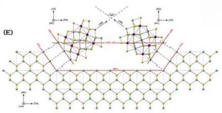
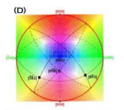
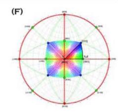
Fig 1) (a) HAADF image of GaAs matrix and precipitates (b) corresponding ASTAR phase map (c) ASTAR orientation matrix along z (d) stereographic projection of monoclinic phase (e) orientation relation between GaAs matric and the completely embedded (Mn,Ga)As crystallite & (f) stereographic projection of cubic GaAs




ASTAR –SEMICONDUCTORS
Ganesh, K J , et al “Automated Local Texture and Stress Analysis in Cu Interconnects Using D- STEM and Precession Microscopy.” Microscopy and Microanalysis, vol 16,no 2,2010,doi:10 1017/S14319276 10061933
STRAIN –SEMICONDUCTORS
A Bashir et al “Strain analysis of a Ge micro disk using precession electron diffraction” J of Applied Physics 2020 DOI: 10 1063/1 5113761
A D Darbal et al “Automated High Precision Strain Measurement Using Nanobeam Diffraction Coupled with Precession” Microscopy & Microanalysis 2013 doi: 10 1017/S1431927613005503
A D Darbal et al “Applications of Automated High Resolution Strain Mapping in TEM on the Study of Strain Distribution in MOSFETs” Microsc Microanal 20 (Suppl 3), 2014 doi:10 1017/S1431927614007053
M.Reisinger et al “Cross-sectional stress distribution in AlxGa1-xN heterostructure on Si(111) substrate characterized by ion beam layer removal method and precession electron diffraction” Materials and Design 106 (2016) 476–481
