High-Tech Instrumentation for the Semiconductor Industry
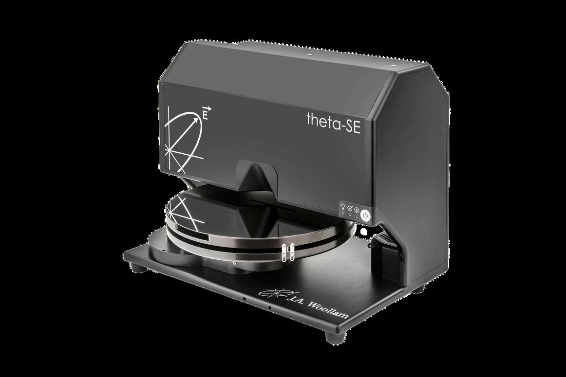
Theta-SE Ellipsometer for Semiconductors
Analyse Electronic Components or Semiconductor Devices using Atomic Force Microscopy
SEMICONDUCTOR METROLOGY
Power
Efficient Control of the Futures Energy
CASE STUDY: STRUCTURE OF MAGNETIC SEMICONDUCTORS
Quantum Design UK and Ireland is part of the Quantum Design International (QDI) group QDI is a global laboratory equipment manufacturer The company distributes scientific and industrial instrumentation through an international network, with subsidiaries in every major technological centre around the world.
WITH CONTENT CONTRIBUTIONS FROM OUR PARTNERS:
Theta-SE Ellipsometer for Semiconductors
Foreword
ThetaSE Ellipsometer for Semiconductors
Semiconductor Testing Solution - E-Lit
X-rays in Semiconductors
Metrology of Optics and Imaging systems
Semiconductor Metrology
Case Study: Structure of Magnetic Semiconductors
Power Electronics – Efficient Control of the Futures Energy
Published Semiconductor Research Using the Quantum Design PPMS VersaLab
Raptor Photonics Launches Camera for PET Semiconductor Inspection
Analyse Electronic Components or Semiconductor Devices using Atomic Force Microscopy
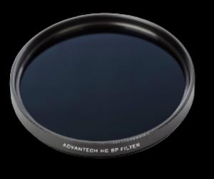
Hard Coat Bandpass Filters for High Performance in Demanding Applications
Further Reading
Bespoke Ellipsometer Measurement for Semiconductor Industry
FOREWORD
Quantum Design (QD) has been a leader in high-tech instrumentation for over 40 years with systems such as the MPMS and VersaLab. We have continually added to our product portfolio by acting as distributor for other market leaders who provide solutions for semiconductors, including J. A. Woollam, InfraTec, Sigray, 4D Technology and Lake Shore Cryotronics
This means we can provide our customers with the right solutions for their semiconductor applications.
Dr. Shayz Ikram
TECHNICAL DIRECTOR
Britain is already amongst the world leaders when it comes to researching and designing semiconductor technology. Semiconductors underpin the ambition to advance quantum, telecom, and AI technologies. QDUKI are proud to be part of that development, strengthening the position through new and innovative solutions.
The Quantum Design UK and Ireland Sales Team
Dr. Luke
Nicholls
TECHNICAL SALES MANAGER
RESULTS AT WAVELENGTHS OF INTEREST FOR
A DESIRED APPLICATION
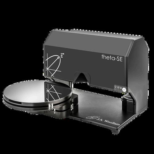
THETA-SE ELLIPSOMETER FOR SEMICONDUCTORS
Since the 1960s, as ellipsometry developed to provide the sensitivity necessary to measure nanometer-scale layers used in microelectronics, interest in ellipsometry has grown steadily Today, the range of its applications has spread to the basic research in physical sciences, semiconductor and data storage solutions, flat panel display, communication, biosensor, and optical coating industries Here we take a look specifically at the J A Woollam thetaSE ellipsometer and its uses for the semiconductor industry
The theta-SE is a push-button spectroscopic ellipsometer for characterising thin film uniformity It features advanced ellipsometry instrumentation in a compact package at an affordable price
For many applications, optical properties are desired at specific wavelengths For example, the semiconductor industry is interested in lithography which requires ellipsometry measurements in the UV region (157nm, 193nm, 248nm, ) The display industry is interested in the visible spectrum Optical coatings require measurement at their design wavelengths, whether at visible, near infrared or even mid-infrared wavelengths Woollam Spectroscopic Ellipsometers cover the spectral range from 33 microns to 140nm This range offers an incredible flexibility that can meet almost any application requirement
Learn more about Woollam thetaSE
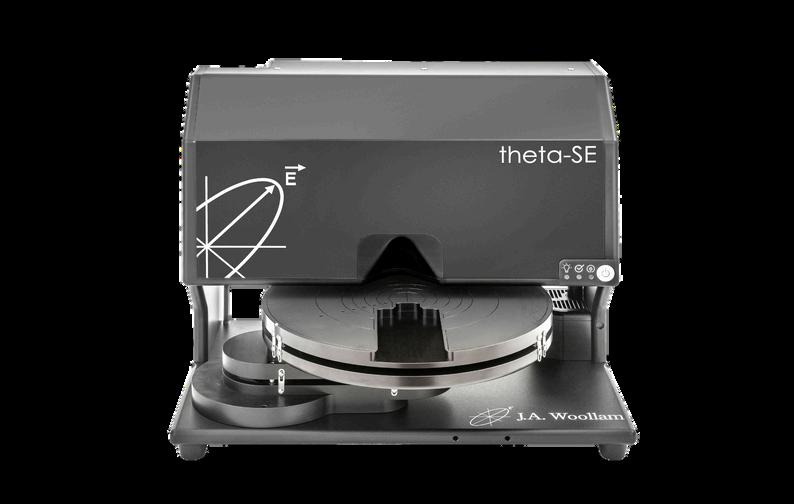
WHY THE THETASE?
FULLY INTEGRATED
The theta-SE comes equipped with 300 mm sample mapping, small-spot measurement beam, fast sample alignment, look-down camera and our latest Dual-Rotation ellipsometer technology The theta-SE has everything you need to measure the spatial uniformity of your film thickness and optical properties
PERFECT FOR:
Dielectrics (oxides, nitrides, carbides)
Polymers (Low-Dielectric constant)
Polysilicon
Multilayers (ONOPO, SOI, )
Lithography Applications
Photoresists
Antireflective coatings
Photomasks
Compound Semiconductors
TECHNICAL PAPERS ON SEMICONDUCTORS
HIGH SPEED
Sample throughput is optimised by using fast point-to-point translation, high-speed sample alignment and Dual-Rotation ellipsometer technology for continuous data collection
COMPACT
The patented, Dual-Theta rotation stage enables full, 300 mm mapping in a small, table-top instrument The instrument footprint is only slightly larger than a 300 mm wafer
USER FRIENDLY
Automated data analysis and built-in reporting enables push-button operation and quick access to measurement results.
AFFORDABLE
The theta-SE delivers the power of spectroscopic ellipsometry and 300 mm uniformity mapping at a reasonable price.
Ellipsometry Characterization of Bulk Acoustic Wave Filters
Authors: E Nolot, A Lefevre, J Hilfiker Phys Stat Sol (c) 5, No5, 17, (2008) 1168-1171
Spectroscopic Ellipsometry (SE) for Materials Characterization at 193 and 157nm
Authors: J Hilfiker, F G Celii, W D Kim, E A Joseph, C Gross, T Y Tsui, R B Willecke, J L Large, and D A Miller Semiconductor Fabtech, 17, (2002) 87-91
Immersion Fluids for Lithography: Refractive Index Measurement Using Prism Minimum Deviation Techniques
Authors: R Synowicki, G Pribil, G Cooney, C Herzinger, S Green, R H French, M K Yang, M F Lemon, J H Burnett, and S Kaplan Semiconductor Fabtech, 22, (2004) 55-58
Spectroscopic Ellipsometry as a Potential In-Line Optical Metrology Tool for Relative Porosity Measurements of Low- K Dielectric Films
Authors: N V Edwards, J Vella, Q Xie, S Zollner, D Werho, I Adhihetty, R Liu, T Tiwald, C Russell, J Vires, and K H Junkerd Mat Res Soc Symp Proceedings, 697, (2002) P471P476
Spectroscopic Ellipsometry Analysis of InGaN/GaN and AlGaN/GaN Heterostructures Using a Parametric Dielectric Function Model
Authors: J Wagner, A Ranakrishnan, H Obloh, M Kunzer, K Köhler, and B Johs MRS Internet J Nitride Semicond Res XX, WYY, (2000)
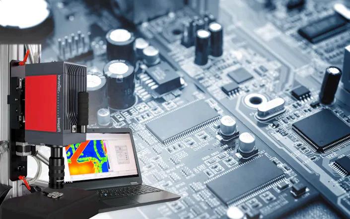
Semiconductor Testing Solution
InfraTec’s E-Lit
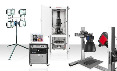
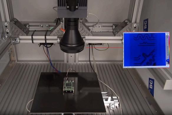
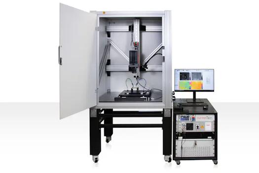
Modular Automated Test Bench
Thermal analysis of electronic and semiconductor devices
Modular test bench for online lock-in measurement
Reliable detection of thermal anomalies in the mK and μK range
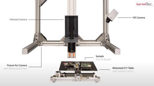
Spatial location of defects in multilayer PCBs and multi-chip modules
Use of thermographic systems with cooled and uncooled detectors
Operational software IRBIS® 3 active with comprehensive analysis options in laboratory conditions
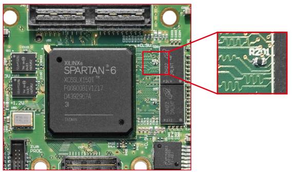
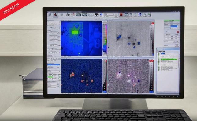
E-LIT – Lock-In Thermography for electronics is an automated testing solution system (as part of NDT techniques) which allows non-contact (electrical) failure analysis of semiconductor material during the manufacturing process. Inhomogeneous temperature distribution, local power loss, leakage currents, resistive vias, cold joints, latch-up effects and soldering issues can be measured with Lock-in Thermography This is achieved by using the shortest measurement times combined with a high-performance thermographic camera and a specialised lock-in procedure.
The power supply for this process is clocked with a synchronisation module and failures that produce mK or even μK temperature differences are reliably detected by the Lock-in Thermography system.
Smallest defects at electronic components like point and line shunts, issues from overheating, internal (ohmic) shorts, oxide defects, transistor and diode failures on a PCB surface, in integrated circuits (IC´s), LED modules and battery cells can be detected and displayed in x and y positions Additionally, it is possible to analyse stacked-die packages or multi-chip modules in z-direction with merely changing the lock-in frequency.
The powerful Lock-in Thermography software uses the latest algorithms and routines from most recent scientific publications
Automated Testing Solution ACTIVE-LIT Failure
Detailed investigation with the help of Multiscanning
Variable parameter settings to analyse different layers and components on a single sample during one measurement run
Analyse your data in real-time with IRBIS® 3 active software
Real-time calculation and visualisation of defect zones
Continuous display of live, amplitude, phase and single phase image
Batch mode / macro editor for automated analysis of sample surface on different layers below the surface Storage and charging of parameters for different samples
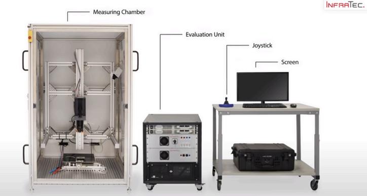
BENEFITS OF THE MODULAR TEST BENCH
Measurement with one workstation - from the entire circuit board to the smallest detail
Customised modular measuring station, e. g. with X-Y table and Z-axis manually or motorised adjustable, for positioning and individual adjustment of the working distances, depending on the size of the measured object
Flexibility through variable components, e.g. different optics, holding devices for the test specimen or contacting options,
Online lock-in measurement with the highest sensitivity
Complete and detailed microscopy analysis
Geometrical resolution up to 1 3 μm per pixel with microscope lenses
Thermal resolution in the microkelvin range
Multi-layer analysis
Automatic scanning of larger samples due to precision mechanics
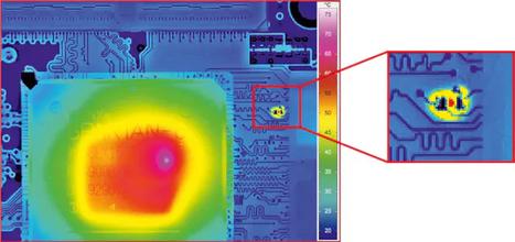
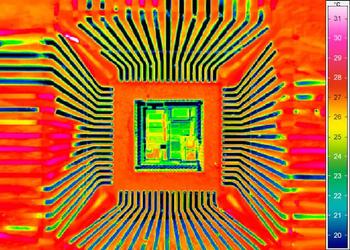
THERMOGRAPHIC IMAGES WITH DIFFERENT OPTICS
100 mm telephoto lens with 500 mm close-up; pixel resolution 75 μm
TALK TO US
Discuss your application and the InfraTec E-LIT Solution with our Technical Sales Manager, Dr Luke Nicholls Call (01372) 378822 Email luke@qd-ukicouk
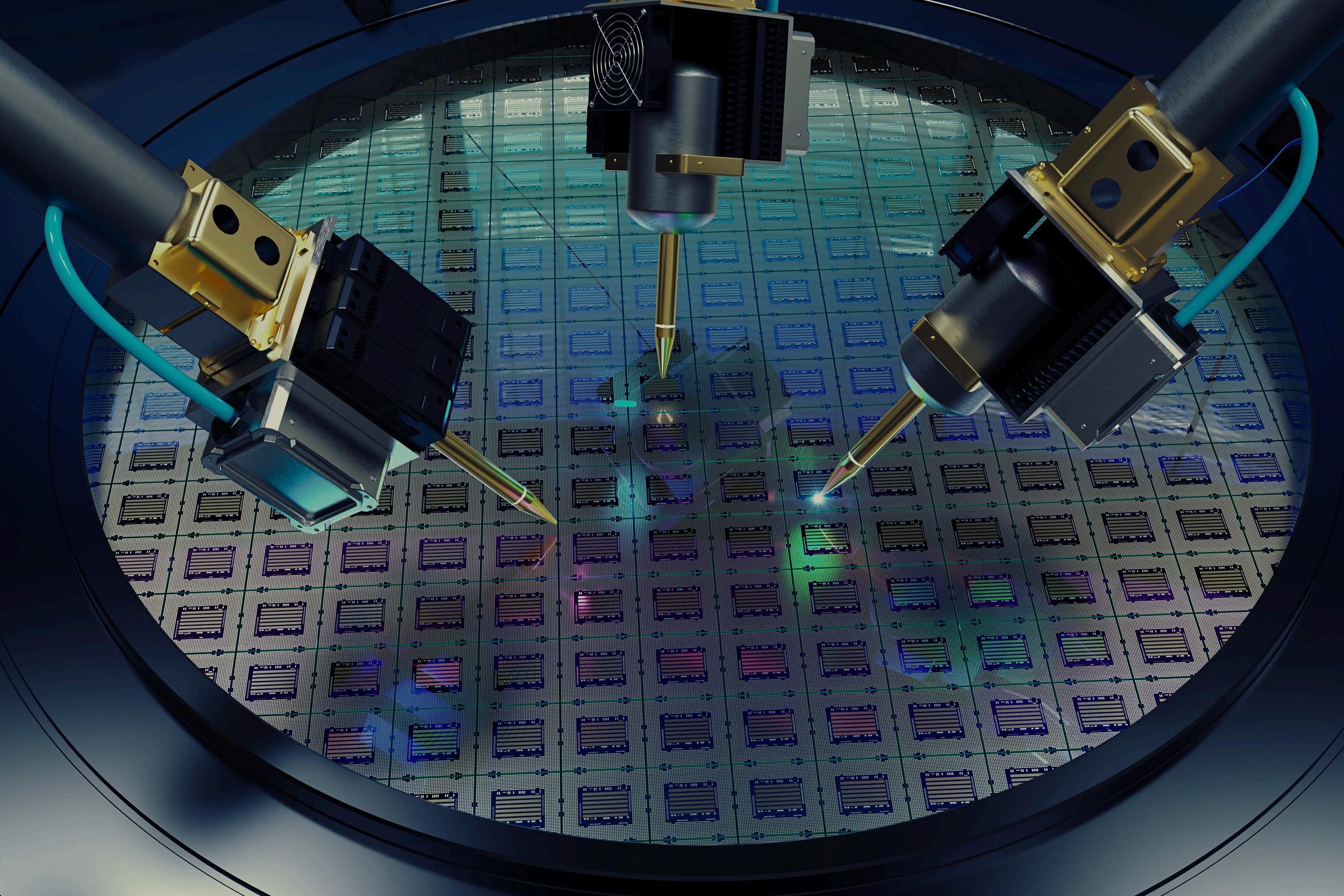
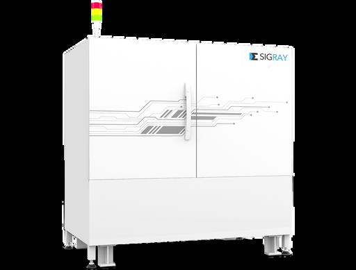
X-RAYS IN SEMICONDUCTORS
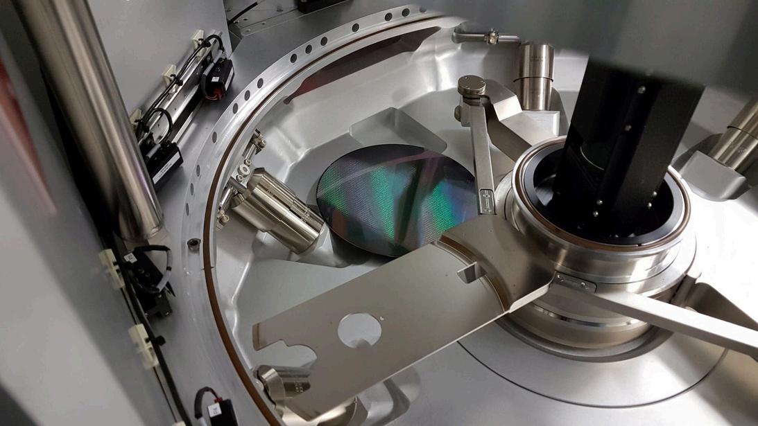
Sigray’s x-ray solutions include 3D x-ray microscopes and microXRF systems in vacuum environments. These systems are used for a range of semiconductor applications, including everything from inspection of wafer contamination and silicon-side process monitoring to failure analysis of packaging.
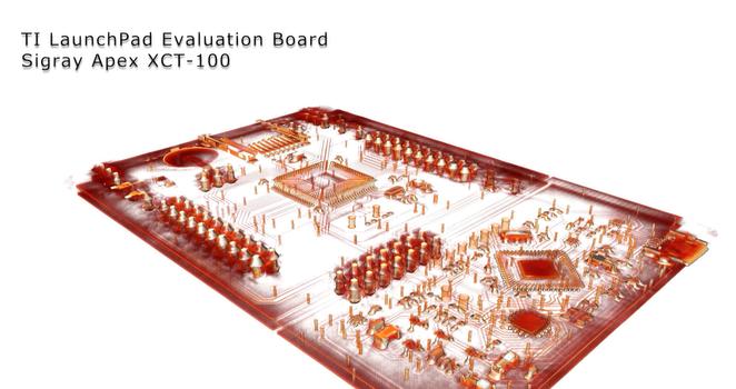
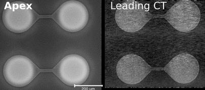
REVERSE ENGINEERING & TRUSTED CIRCUIT
Sigray’s Apex XCT-150 provides 0 5 um resolution 3D imaging of large PCBs and packages within minutes for reverse engineering and trusted circuit applications Complete montages of intact packages of 200 cm x 200 cm are possible at spatial resolutions down to 0 5 um.
WAFER LEVEL PACKAGING
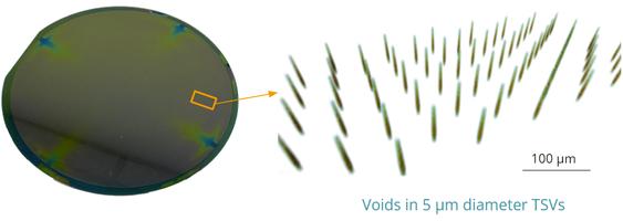
Apex XCT-150 enables intact wafer imaging for next-generation packaging schemes. The system is successfully used for submicron failures such as voids, non-wets, cracks, etc in TSVs, hybrid microbumps, and solder.
Voids clearly rendered in 5 um TSVs within minutes Imaged within an intact 300mm wafer on the Apex XCT
Sigray Apex XCT-150
Rethink Impossible
Sub-Micron 3D X-ray In Minutes Advanced semiconductor packaging & FA
3D Imaging on Intact Samples Up to 300 mm Diameter
0 5 µm 3D Spatial Resoluti No Beam Hardening Artifa
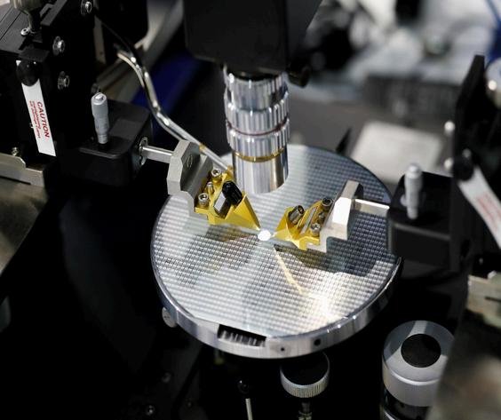
For UV, EUV, and X-ray wavelength applications, optics must be extremely smooth to avoid scattering, which affects image quality, signal-to-noise, and other critical optical performance properties. The typically high incident energy can also degrade optics quickly. Thus, manufacturers and end users require a reliable, reproducible method to verify smoothness to subnanometerlevels.
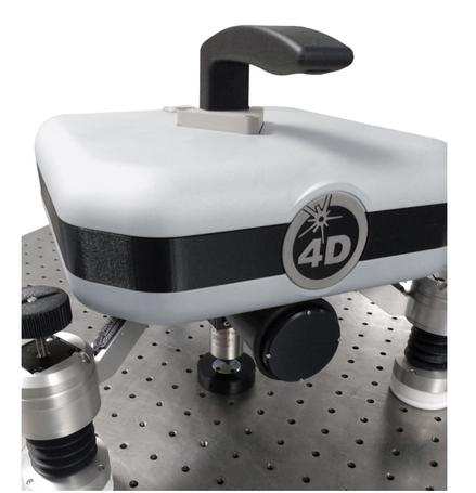
But, while newer manufacturing techniques have enabled production of supersmooth optics, the metrology to accurately measure these surfaces has lagged behind. To fill the void, the NanoCam HD optical profiler (Figure 1) has been proven to provide reliable, noncontact measurement of supersmooth surfacetexture,insituontheshopfloor.
"Because 4D’s dynamic technology is the best way to obtain good measurements in extreme environments, we offer the best choices and the greatest experience in measuring in these circumstances."
THE CHALLENGE OF MEASURING SUPERSMOOTH OPTICS
“Supersmooth” surfaces typically have an RMS roughness (Sq) of less than 0 1 nm Measuring such extremely smooth surfaces exceeds the capability of most measurement technologies.
Figure 1 UV, EUV, and X-ray optics, such as the mirrors in this ring laser gyro, require supersmooth surfaces to avoid scattering that can impact performance and degrade the optics (Rogoway)
To date, stylus-based instruments and atomic force microscopes have been used. However, these techniques are very slow, and the contacting probes can damage the surfaces. Additionally, the measurement systems require highly controlled environments because vibration, shop noise, and air turbulence will degrade measurements
Non-contact, optical profiling is the preferred method for quickly acquiring 3D data of supersmooth surfaces. Scanning white light optical profilers are most common. But the noise floor of scanning systems is typically too high to measure sub-angstrom roughness, even using phase-shifting interferometry (PSI) mode.
NANOCAM HD MEASURES SUPERSMOOTH SURFACES
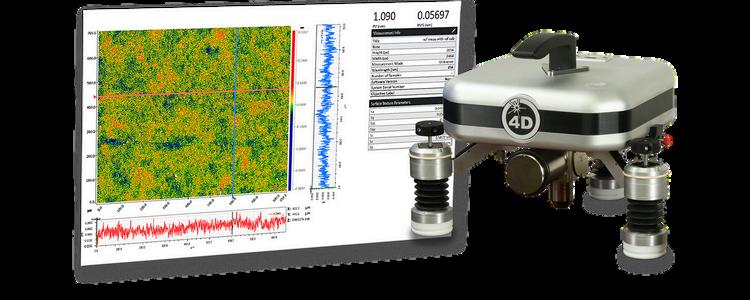
4D Technology’s NanoCam HD is an enabling technology for controlling the production of supersmooth surfaces The NanoCam HD (Figure 2) offers several benefits that make sub-angstrom measurement possible.
DYNAMIC INTERFEROMETRY
In recent years, vibration-immune “dynamic” interferometry has been adapted for roughness measurement. In dynamic instruments such as 4D Technology’s NanoCam HD, all measurement data is acquired simultaneously, rather than sequentially as in scanning methods. Such fast acquisition enables the NanoCam HD to measure in shop floor environments without expensive vibration isolation.
Learn more about 4D Technology
Tel:(01372)378822 Email:luke@qd-ukicouk
Semiconductor Metrology
Electronic components are everywhere in our modern world. These components must be reliable, as they control critical systems from everyday items to electronically controlled military equipment and various aerospace equipment.
To assure this reliability, components must go through a battery of tests. XRF analysis is an irreplaceable tool for the semiconductor industry to guarantee and certify their products.
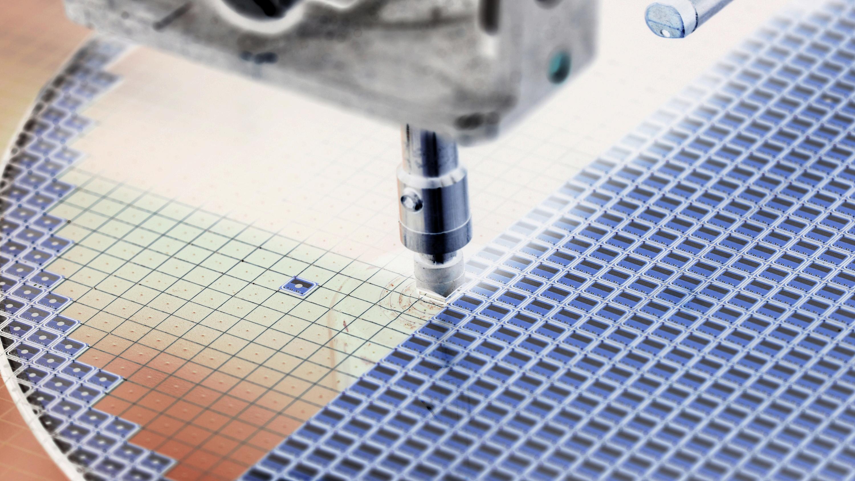
Electrical or photonic circuits are one of these components that are the foundation for so many other products. These circuits begin their lives on silicon wafers. As the wafers and associated circuits and boards become more specialised, they require different types of testing.
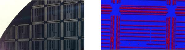
IXRF Systems offers a 5µm spot size, the smallest on the market, allowing for extremely high resolution maps, analysis of small leads or pillars. Though SnPb solder has its place in technology, there is now a shift to use SnAg due to environmental, health and safety concerns These solder points must also be tested
TALK TO US
Discuss your application and the IXRF Systems range of products with our Sales Manager Dr Luke Nichoklls
Call: (01372) 378822
Email: luke@qd-ukicouk
Current technologies include Pb-free bumps of SnAg, as well as Pb-free SnAg pillars on Cu seed. Current bump/pillar and seed sizes are about 50 to 150µm. However, next-generation technology is pushing towards smaller pillar/seed sizes of 20- 30µm.
Leads on electronic components cannot fail, less the whole system will fail A wellknown phenomenon known as ‘whiskers’ can cause these components to fail. The whiskers come from tin used in electronic component surfaces.
It has been found that adding lead to the tin can prevent the growth of whiskers This addition of lead must be analytically measured to ensure expected and required concentrations. Most aerospace companies require a minimum of 3% Pb to prevent tin whiskers.
XRF is the preferred method for lead testing in tin. XRF is more accurate than EDS based on the larger area and depth of measurement.
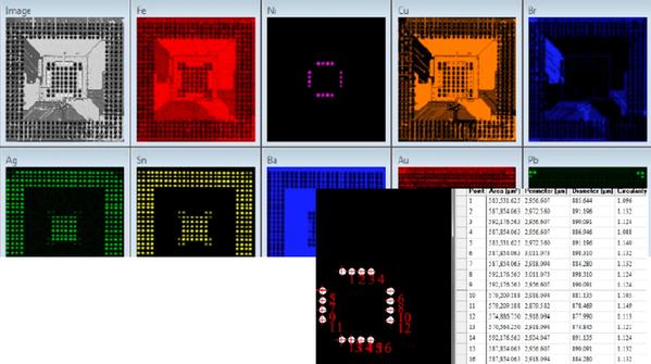
IXRF Systems’ powerful software can quickly identify, measure, and analyse multiple solder bumps on a board
Quantitative analysis was done on one of the SnPb solder bumps in the centre trio section, a circled portion in the elemental map (fig. 2).
IXRF Systems’ ATLAS SEMI can analyse for:
Bump inspection
CMOS image sensors (CIS)
Corrosion resistance coating
Cu CMP control at BEOL
Film stack
Light elements
Metal film stack composition such as CIGS
Multi-stack structures
Pb measurement for Whiskers
Redistribution layer (RDL)
Sn/Ag Bump/Pillar measurements
Sputtering targets
Thermal barrier coating
Thick mono-layers
Thickness and composition control
Thin Film/Coating thickness
measurements
Ultra-thin films
Under bump metallisation (UBM)
Wafer-level packaging (WLP)
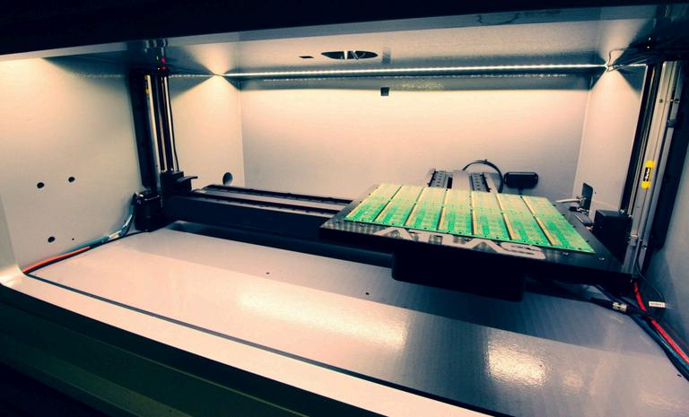
Fig. 2 An elemental map of a large wafer area with pillars, collected with a 5µm spot size.
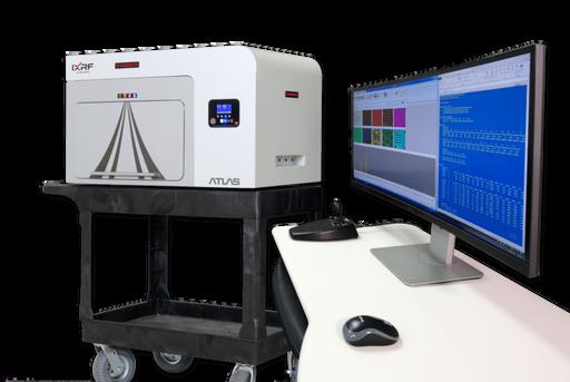
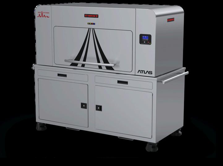
IXRF Systems’ ATLAS SEMI is the very latest micro spot energy dispersive X-ray fluorescence (micro XRF) imaging spectrometer for semiconductor metrology
Biggest chamber
features the industry’s most voluminous sample chamber, allowing for automation of more samples, larger area mapping capabilities, and wider variability of sample types
The 5 micron advantage
With the smallest X-ray spot in the industry at 5 microns, ATLAS SEMI is optimised for analysis speed without compromising accuracy.
Unmatched speed
Mix and match up to 4 Silicon Drift Detectors (SDD). For the largest possible solid angle collection efficiency Up to 600 mm2 active area Highest count rate with the smallest spot for fast high-res images
Housler et al
MC2011 Kiel Electron Microscopy Proceed
Magnetic semiconductor materials have attracted widespread attention in recent years due to their potential applications for the transport of information by exploiting both the intrinsic spin of the electron and its associated magnetic moment, in addition to its fundamental electronic charge. The new technology which emerged from discoveries in the 1980s concerning spin-dependent electron transport phenomena in solid-state devices was called Spintronics ('Spin Transport Electronics') also known as magnetoelectronics.
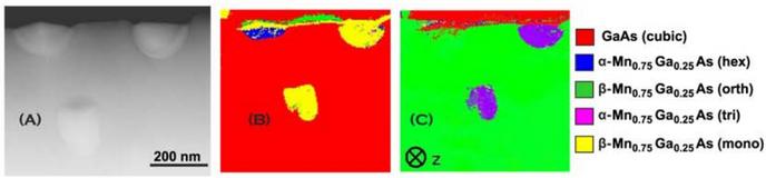
The material system (Mn,Ga)As on GaAs is of great interest for the development of such spintronic devices because the unstrained-bulkMnAs is ferromagnetic at room temperature (αMnAs, P6Jmmc). It undergoes a phase transition to paramagnetic phases at 40°c ( β-MnAs, Pnma) and above 125°C (y-MnAs, P6,/mmc)). "Surface contactable quasi-embedded" MnAs crystallite precipitates are formed in a [001] - oriented GaAs matrix during the cooling down stage of a MnAs layer that was deposited by metal-organic chemical vapour deposition (MOCVD) above 600 °c
In order to obtain a thorough understanding of the (Mn,Ga)As crystallite formation process, the crystallographic phase and orientation of the precipitates with respect to the matrix have to be determined. The chemical composition of the precipitates was determined by quantitative EDXS analysis , their chemical composition was defined as Mn₀₇₅Ga₀₂₅As
The Challenge:
Identify unknown phase of MnGaAs precipitates among 4 different crystal phases & establish orientation relation between GaAs matrix and precipitates
The Solution:
ASTAR technique coupled with precession electron diffraction
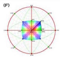
A careful inspection of the PED diagrams on the precipitates showed that there existed super structure reflections not consistent with MnAs bulk structure ASTAR template matching analysis with all possible templates of 4 possible phases compatible with Mn₀₇₅Ga₀₂₅As (total 38561 templates) shows a coexistence of precipitates with the monoclinic β-phase (space group P2,/m) and of precipitates with the hexagonal α-phase (P6,/mmc) at room temperature. An example of ASTAR phase and orientation analysis of the embedded (Mn, Ga)As-crystallite precipitates in GaAs is illustrated below.
(A) HAADF image of GaAs matrix and precipitates (B) corresponding ASTAR phase map
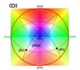
(C) ASTAR orientation matrix along z (D) stereographic projection of monoclinic phase
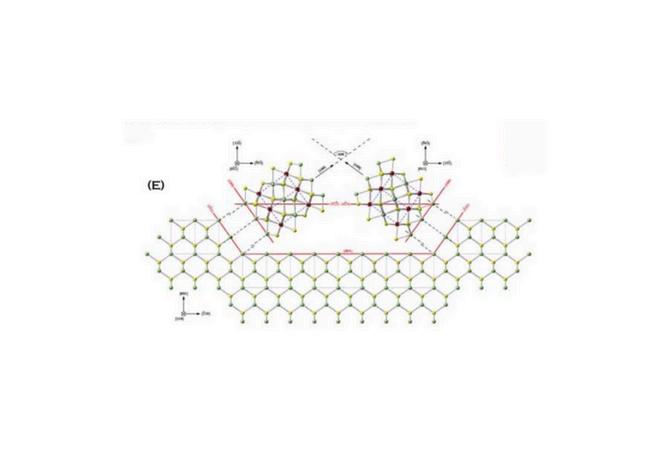
(E) orientation relation between GaAs-matrix and the completely embedded (Mn,Ga)As crystallite & (F) stereographic projection of cubic GaAs
SPINTRONIC DEVICE PROPERTIES
Experimental Data: TEM type: Jeol 2200
FS Map resolution: 1 nm Scanned area: 2 x 2 µm
Crystal Structure: GaAs: Cubic, F43m a= 5.56Å
STRONGLY DEPEND ON A NANOMETER SCALE
STRUCTURE
Learn more about the NanoMEGAS A-Star TEM Orientation Imaging
TALK TO US
Mn₀₇₅Ga₀₂₅As: hexagonal,P6,/mmc
Discuss your application and the Nanomegas range of products with our Technical Director, Dr Shayz Ikram Call (01372) 378822 Email shayz@qd-ukicouk
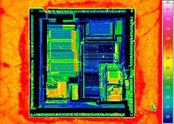
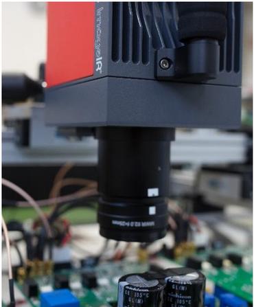
THERMOGRAPHY IN USE FOR HIGH-PERFORMANCE ELECTRONIC SYSTEMS
The energy efficiency of electronic components is becoming increasingly important in numerous fields of application And that is not all: in our electronic and high-tech age, the demand is for even faster active components, higher power densities of miniaturised systems as well as absolute reliability Along with this, there is the request for environmentally conscious resource procurement and the requirement that the increase in performance of modules should run parallel to lower energy consumption. For this reason, the electronics industry has relied on silicon (Si) for more than 50 years However, this is now reaching its physical limits
The demands for more efficient and environmentally aware electronics, for example in data centres and in the development of electric cars, are growing steadily Therefore, energy efficiency is becoming a strategic issue for wide areas of industry, and the semiconductor material gallium nitride (GaN) is becoming one of the key components in the field of renewable energies
Silicon-based microelectronics have repeatedly reached new performance peaks in recent years The number of transistors on a chip doubled almost every two years and so did the computing power of processors But the limits have almost been reached, which is why the Institute of Electrical Engineering and Information Technology (ET&IT) and the Institute of Materials Science are working on new semiconductor materials.
These are two of the three institutes of the Faculty of Technology at Christian-Albrechts-Universität zu Kiel (CAU Kiel) Research topics of this faculty include renewable energy, sensor technology and electromobility
FUTURE SEMICONDUCTOR MATERIALS - NEW OPPORTUNITIES AND CHALLENGES
More powerful semiconductor materials are the prerequisite for the electronics market of the future in general and for power electronics in particular Electronic systems should perform better and at the same time require less energy
This is a goal that manufacturers of electric cars, for example, have defined for themselves The procurement of the resources used should be as environmentally friendly as possible and their use as efficient as possible
Fig 1: Prof Dr -Ing Marco Liserre, Head of the Chair of Power Electronics, and his team developed the prototype of an intelligent transformer that controls the current flow
Kiel University Christian-Albrechts-Universität zu Kiel, Faculty of Technology, Chair of Power Electronics https://www uni-kiel de/en/ M Sc Johannes Kuprat
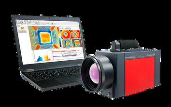
Prof Dr -Ing Marco Liserre Thermal imaging system: ImageIR® 8300 infrared camera
What is required now are more powerful semiconductor materials for significantly smaller components For this reason, power semiconductors such as gallium nitride (GaN) and silicon carbide (SiC) are overtaking silicon (Si), which has been used up to now. GaN transistors in particular enable a smaller size and potentially generate lower costs.
They have a significantly lower conductive resistance for the same size of electronic components and achieve faster commutations, which in turn results in lower switching losses The lack of reverse recovery charging also allows for higher frequency and power density All of the above factors offer significantly higher energy efficiency than silicon-based technology
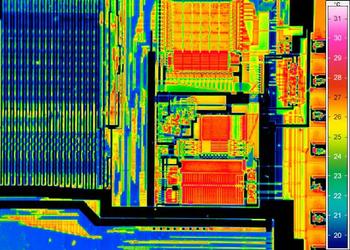
THERMOGRAPHY IN USE FOR POWER ELECTRONICS
Since both the electronic components and the transistors are very small, the infrared camera to be used must meet certain requirements
For this reason, a measurement set-up suitable for this purpose was designed for the CAU, in which a cooled thermography system of the ImageIR® infrared camera series from InfraTec is used. With its high thermal resolution, it detects even the smallest temperature changes and, due to its excellent geometric resolution, resolves structures of less than 50 µm in size in this application even with standard lenses The ImageIR® infrared camera used has a cooled photon detector enabling the imaging of particularly fast processes Switching peaks can thus be analysed without any problems The noncontact measurement is non-destructive and enables the detection of several critical points, as the complete object is imaged A further advantage is the non-complicated MATLAB interface via the IRBIS® Software Development Kit (SDK) from InfraTec
Scientists at the Faculty of Technology at Christian Albrechts University (CAU) in Kiel are making use of these advantages The changes and developments of temperatures and their distribution in various semiconductor materials in the field of power electronics are being researched here in order to optimise processes and techniques
Fig 2: Thermal setup with infrared camera and open semiconductor modules for thermal evaluation of the semiconductors during operation
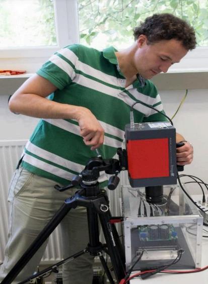
Fig 3: Dr Markus Andresen setting up the InfraTec infrared camera for tests to validate active thermal control
In particular, it is about U-Heart: a new concept of isolated DC-DC converters with multiple connections, which were developed to achieve the highest reliability together with high energy efficiency with minimal redundancy. It is equipped with a fault detection circuit that excludes a detected faulty cell from power transmission
The ImageIR® infrared camera used has a cooled photon detector enabling the imaging of particularly fast processes Switching peaks can thus be analysed without any problems The noncontact measurement is non-destructive and enables the detection of several critical points, as the complete object is imaged A further advantage is the non-complicated MATLAB interface via the IRBIS® Software Development Kit (SDK) from InfraTec
“Self-healing” approaches are actually under development to maintain the operation of all cells and to continue operating at full power: "self-healing" allows the inverter to continue operating at full power. Thus, U-Heart is a ERC grant for a proof of concept for a maintenancefriendly power converter and can be used as a multi-port converter connecting multiple voltage grids, e g energy storage systems (batteries, supercapacitors), renewable energy sources (solar PV modules, fuel cells, etc ) and DC loads
The development of this energy superstar also benefited from insights gained through thermography from the predecessor project Heart (ERC grant)
In general, it is reasonable to use thermographic cameras already in the development and creation process of new electronic components Valid and meaningful data about the heat development in the components is obtained This again allows, among other things, conclusions to be drawn about the performance and energy efficiency of a module, and faults are reliably detected at an early stage and can be rectified
Want
Contact our Technical Sales Manager: Dr. Luke Nicholls
Telephone: (01372) 378822
Email: luke@qd-uki.co.uk
Large detector enables highest sensitivity (1,280 × 1,024) IR pixels by genuine camera hardware
Analysis of extreme temperature changes and gradients in full frame
Highly accurate and repeatable measurements
High-speed, long-distance interference proof data transmission
Flexible setting of temperature measurement ranges/integration times beyond calibration ranges
Facilitates the analysis of objects with extreme temperature gradients
InfraTec Image IR Series Thermography Cameras
High-speed thermography systems
Precise radiometric calibration
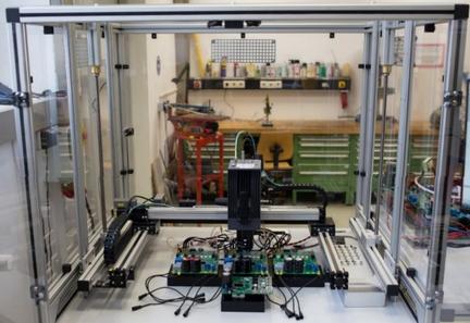
Fig 4: Measurement set-up for the analysis of different semiconductor materials in the laboratory of CAU Kiel
Transport Anisotropy of Epitaxial VO 2 Films near the Metal–Semiconductor Transition
Kittiwatanakul, Salinporn and Lu, Jiwei and Wolf, Stuart A., Applied Physics Express, 4 (9), 1882-0786 (2011), DOI.
Abstract
We report a very large anisotropy in the dc conductivity of epitaxial VO2 thin films deposited on a single-crystal (100) TiO2 substrate There was a large tensile strain along the c-axis and a compressive strain along the a-axis of rutile VO2 due to the lattice mismatch between VO2 and TiO2. The in-plane conductivity was measured along <010> and <001> of VO2, and it is found that the conductivity anisotropy ratio σ<001>/ σ<010> was 41 5 at 300 K, much larger than that of single-crystal VO2 --------
Thermoelectric transport and Hall
measurements of low defect Sb₂Te₃ thin films grown by atomic layer deposition
Zastrow, S. and Gooth, J. and Boehnert, T. and Heiderich, S. and Toellner, W. and Heimann, S. and Schulz, S. and Nielsch, K., Semiconductor Science and Technology, 28(3), 035010 (2013), DOI.
Abstract
Sb2Te3 has recently been an object of intensive research since its promising applicability in thermoelectric, in phase-change memory devices and as a topological insulator. In this work, we report highly textured Sb₂Te₃ thin films, grown by atomic layer deposition on Si/SiO₂ wafers based on the reaction of SbCl₃ and (Et₃Si)₂Te
The low deposition temperature at 80 °C allows the pre-patterning of the Sb₂Te₃ by standard lithography processes A platform to characterise the Seebeck coefficient S, the electrical conductivity σ as well as the Hall coefficient RH on the same film has been developed Comparing all temperature-dependent transport properties, three different conductive regions in the temperature range of 50–400 K are found Room temperature values of S = 146 × 10 ⁶ VK ¹ , σ = 10⁴ Sm ¹ and mobility µ = 270 5 × 10 ⁴ m² V ¹ s ¹ are determined The low carrier concentration in the range of n = 2.4 × 10¹⁸ cm ³ at 300 K quantifies the low defect content of the Sb₂Te₃ thin films
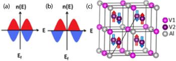
Antiferromagnetic phase of the gapless semiconductor V₃Al
Jamer, M. E. and Assaf, B. A. and Sterbinsky, G. E. and Arena, D. and Lewis, L. H. and Sa\'ul, A. A. and Radtke, G. and Heiman, D., Phys. Rev. B, 91(9), 094409 (2015), DOI.
Abstract
Discovering new antiferromagnetic (AF) compounds is at the forefront of developing future spintronic devices without fringing magnetic fields. The AF gapless semiconducting D0₃ phase of V₃Al was successfully synthesised via arc-melting and annealing
Figure 1 Illustrations of the DOS for (a) a gapless semiconductor and (b) a SGS (c) The D0₃ structure of V₃Al has an Al-V2-V1-V2-Al configuration along the body diagonal and is an AF gapless semiconductor The up (red) and down (blue) arrows correspond to atoms with positive and negative spins, respectively
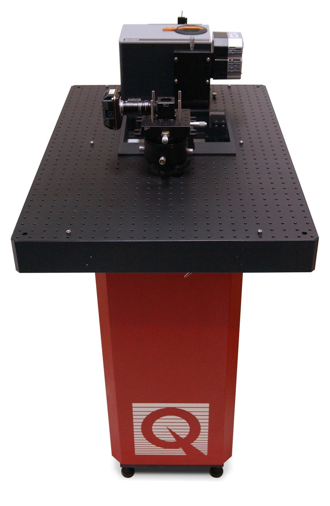
Quantum Design VersaLab™ Measurement System
Cryogen-free Physical y Measurement System
Contact our Technical Director: Dr. Shayz Ikram
(01372) 378822
With a temperature range of 50 – 400 K, this 3 Tesla platform is perfect for accomplishing many types of materials characterisation in a limited space.
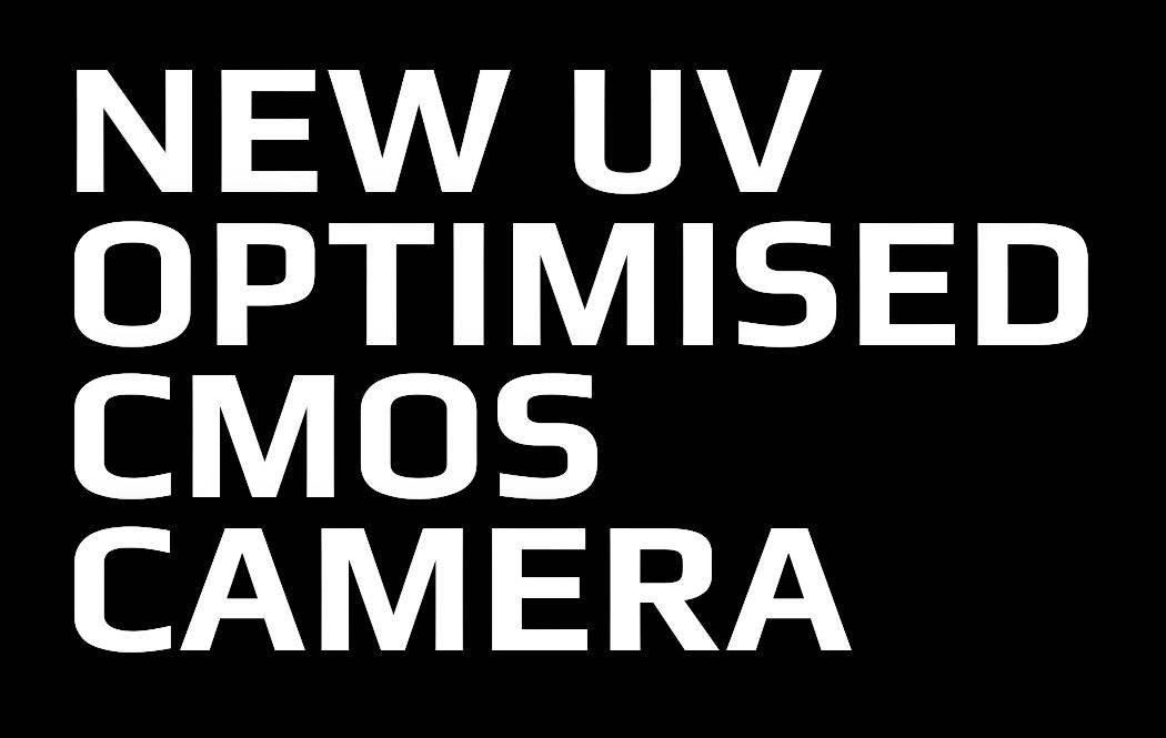
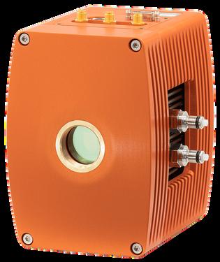
QDUKI's photonics partner, Raptor Photonics launches camera for PET semiconductor inspection
RaptorPhotonicshaslaunchedtheHawkIndigo, using a next generation 2/3” CMOS sensor, enabling ultimate UV sensitivity and high QE of 36% at 250nm With a pixel size of 274µm, the cameraachievesaresolutionof81MPandoffers global shutter, progressive scan technology to enables real time, lag-free images at 15Hz fullframethroughaCameraLinkinterface.
TheHawkIndigoisextremelyruggedandcanbe usedinharshenvironments,workingfrom-20°C to +55°C, with more extreme temperatures on special request It is ideal for integration into industrial applications offering greater precision in hyperspectral imaging, transparent materials (plastic and PET), semiconductor, wafer and mask inspection, material sorting, combustion imagingandhighvoltagetechnology
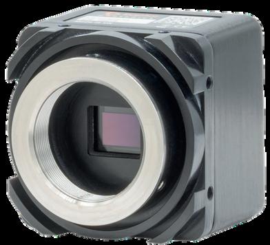
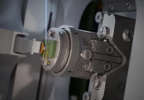
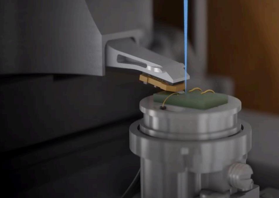
By combining the complementary strengths of AFM and SEM, FusionScope opens the door to a world of new application possibilities
Learn more about the QD FusionScope
FusionScope is an easy-touse correlative microscopy platform designed from the ground up to add the benefits of SEM imaging to a wide range of AFM measurement techniques.
TALK TO US
Discuss your application and the QD FusionScope with our Sales Manager, Dr Luke Nicholls Call (01372) 378822 Email luke@qd-ukicouk
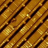
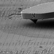
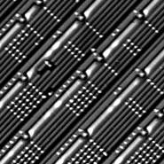
ANALYSE ELECTRONIC COMPONENTS OR SEMICONDUCTOR DEVICES USING ATOMIC FORCE MICROSCOPY
Detailed location and analysis of nanometer-sized structures is a challenging and time-consuming task for all AFM operators. The size reduction in recent generations of transistors creates especially high demands on quality control and failure analysis.
With FusionScope and Profile View you can easily navigate the cantilever tip to the region of interest and perform high resolution AFM analysis of your sample. Measure the real 3D topography with subnanometer resolution or extract additional information using conductive AFM
ANDOVER CORPORATION ADVANTECH™ LINE OF HARD COAT BANDPASS FILTERS FOR HIGH PERFORMANCE IN DEMANDING APPLICATIONS
Andover Corporation, a world leader in the design and manufacture of optical
These hard coat filters are manufactured using a magnetron-sputtered hard oxide coating precisely deposited without any absorbing filter glass. This coating produces optical filters that are thinner and lighter weight while providing greater resistance to extreme temperatures, humidity, scratching and other environmental hazards.
durability and long life for demanding applications, such as spectroscopy, fluorescence, imaging and sensing in the biomedical, machine vision and semiconductor industries
ADVANTECH first surface bandpass filters provide transmission rates over 90% at wavelengths from 337-1200 nm.
Additionally, hard oxide coatings are known to extend filter life to as long as 30 years. ADVANTECH hard coat filters are available in three standard sizes and mounted in an anodised aluminum ring.
ADVANTECH thin films can be customised and applied to a wide range of substrate materials to achieve deep blocking and high transmission for various application requirements With a staff of in-house engineers, advanced testing capabilities and custom fabrication options, Andover is uniquely qualified to meet and exceed customers' needs for high performance and exceptional value.
"Andover is well known for its commitment to high quality and worldclass customer service. We are excited to add
ADVANTECH to our
everexpanding line of hard coat and traditional optical filters so our customers can continue to excel at bringing cutting-edge technology to their markets."
Michael Tiner, COO of Andover Corporation
MICHAEL TINER, COO OF ANDOVER CORPORATION
You might also like:
These specialised filters are custom parts mass ordered throughout the years. They're highly utilised in a wide range of industries and applications, including; semiconductor photoresist removal (ANDV4442, ANDV4565)
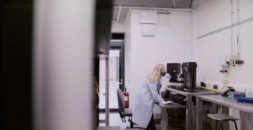
Seeking to better understand the optical and electronic properties of materials or thin films for nanophotonic or electronic applications?
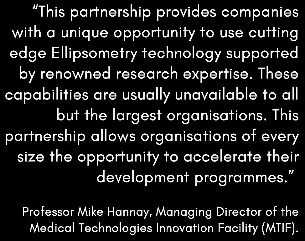
The partnership agreement between QDUKI and the Medical Technology Innovation Facility, affords customers the ability to view and utilise the JA Woollam IR VASE II Spectroscopic Ellipsometer
Indeed, this is only one of two such instruments in the UK and the only one now made available to customers in the UK in this way The nature of Ellipsometry (relatively fast and non-destructive) makes it ideal for diagnostics in several sectors such as semiconductor devices, photovoltaics, nano-photonics, flat panel displays, optical coating stacks, construction materials, biological and medical coatings, protective layers as well as real-
MTIF – with a strong academic pedigree and expertise in nanofabrication – can conduct such analysis on your behalf offering a bespoke and individualised service Please reach out to discuss your needs today
A variety of assistive technologies for materials deposition, including physical and chemical deposition techniques, such as RF magnetron sputtering, atomic layer deposition and thermal evaporation of nano-engineered coatings and thin films. These are applicable across a broad range of industrial applications such as, optical coatings, plasmonic thin films, SERS sensors and large-area electronic devices
Want to learn more about Ellipsometry?
Compound Semiconductors
Electronic Transport Characterisation of HEMT Structures