2 minute read
ANALYSE ELECTRONIC COMPONENTS OR SEMICONDUCTOR DEVICES USING ATOMIC FORCE MICROSCOPY


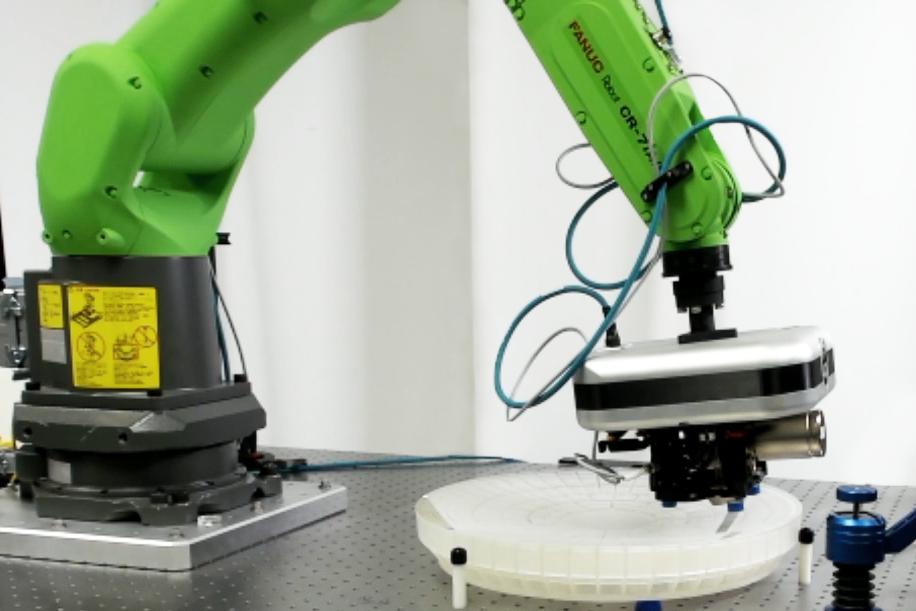
Detailed location and analysis of nanometer-sized structures is a challenging and time-consuming task for all AFM operators. The size reduction in recent generations of transistors creates especially high demands on quality control and failure analysis.
By combining the complementary strengths of AFM and SEM, FusionScope opens the door to a world of new application possibilities

FusionScope is an easy-to use correlative microscopy platform designed from the ground up to add the benefits of SEM imaging to a wide range of AFM measurement techniques.
With FusionScope and Profile View you can easily navigate the cantilever tip to the region of interest and perform high resolution AFM analysis of your sample. Measure the real 3D topography with subnanometer resolution or extract additional information using conductive AFM.


Learn more about the QD FusionScope