4 minute read
Semiconductor Metrology


Electronic components are everywhere in our modern world. These components must be reliable, as they control critical systems from everyday items to electronically controlled military equipment and various aerospace equipment.
To assure this reliability, components must go through a battery of tests XRF analysis is an irreplaceable tool for the semiconductor industry to guarantee and certify their products.
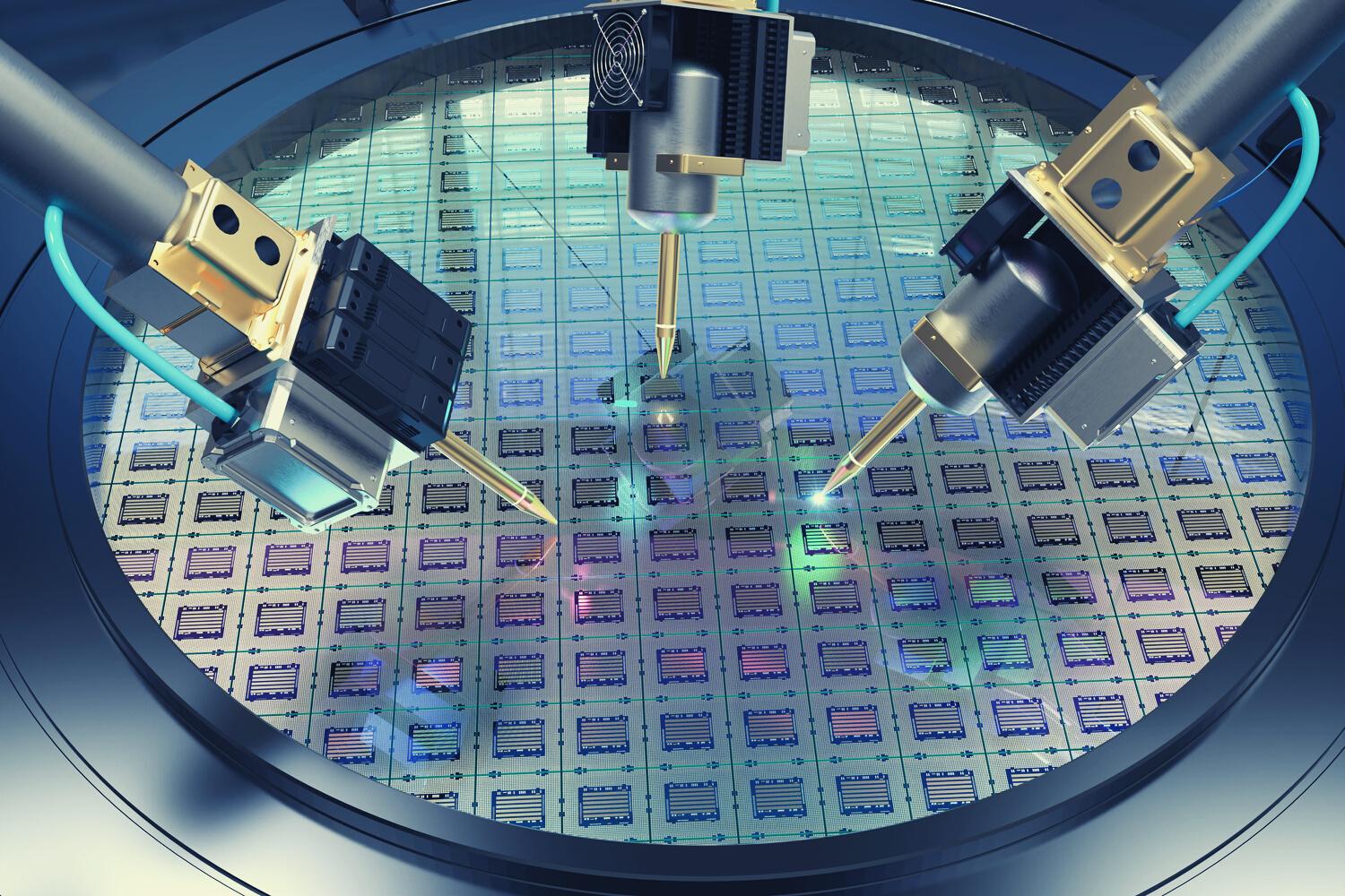
Electrical or photonic circuits are one of these components that are the foundation for so many other products These circuits begin their lives on silicon wafers. As the wafers and associated circuits and boards become more specialised, they require different types of testing.
IXRF Systems offers a 5µm spot size, the smallest on the market, allowing for extremely high resolution maps, analysis of small leads or pillars. Though SnPb solder has its place in technology, there is now a shift to use SnAg due to environmental, health and safety concerns. These solder points must also be tested.
Current technologies include Pb-free bumps of SnAg, as well as Pb-free SnAg pillars on Cu seed. Current bump/pillar and seed sizes are about 50 to 150 µm. However, next-generation technology is pushing towards smaller pillar/seed sizes of 20- 30 µm
Leads on electronic components cannot fail, less the whole system will fail. A well-known phenomenon known as ‘whiskers’ can cause these components to fail. The whiskers come from tin used in electronic component surfaces.
It has been found that adding lead to the tin can prevent the growth of whiskers. This addition of lead must be analytically measured to ensure expected and required concentrations Most aerospace companies require a minimum of 3% Pb to prevent tin whiskers.
XRF is the preferred method for lead testing in tin. XRF is more accurate than EDS based on the larger area and depth of measurement.
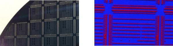
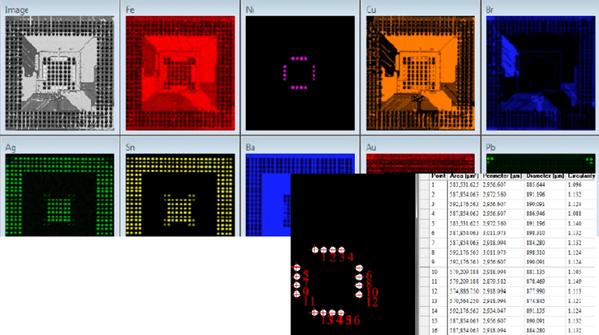
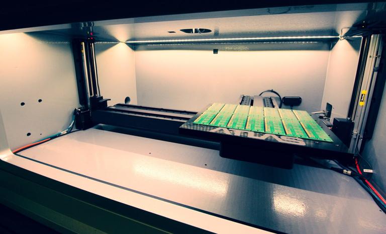
IXRF Systems’ powerful software can quickly identify, measure, and analyse multiple solder bumps on a board.
Quantitative analysis was done on one of the SnPb solder bumps in the centre trio section, a circled portion in the elemental map (fig. 2).
IXRF Systems’ ATLAS SEMI can analyse for:
Bump inspection
CMOS image sensors (CIS)
Corrosion resistance coating
Cu CMP control at BEOL
Film stack
Light elements
Metal film stack composition such as CIGS
Multi-stack structures
Pb measurement for Whiskers
Redistribution layer (RDL)
Sn/Ag Bump/Pillar measurements
Sputtering targets
Thermal barrier coating
Thick mono-layers
Thickness and composition control
Thin Film/Coating thickness measurements
Ultra-thin films
Under bump metallisation (UBM)
Wafer-level packaging (WLP)
Biggest chamber...
... features the industry’s most voluminous sample chamber, allowing for automation of more samples, larger area mapping capabilities, and wider variability of sample types
IXRF Systems’ ATLAS SEMI is the very latest micro spot energy dispersive X-ray fluorescence (micro XRF) imaging spectrometer for semiconductor metrology
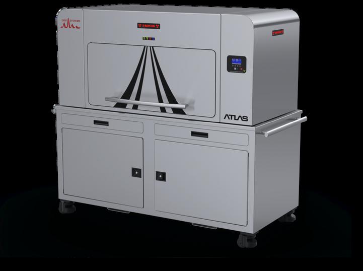
The 5 micron advantage
With the smallest X-ray spot in the industry at 5 microns, ATLAS SEMI is optimised for analysis speed without compromising accuracy.
Unmatched speed
Mix and match up to 4 Silicon Drift Detectors (SDD). For the largest possible solid angle collection efficiency Up to 600 mm2 active area Highest count rate with the smallest spot for fast high-res images
Magnetic semiconductor materials have attracted widespread attention in recent years due to their potential applications for the transport of information by exploiting both the intrinsic spin of the electron and its associated magnetic moment, in addition to its fundamental electronic charge The new technology which emerged from discoveries in the 1980s concerning spin-dependent electron transport phenomena in solid-state devices was called Spintronics ('Spin Transport Electronics') also known as magnetoelectronics.
The material system (Mn,Ga)As on GaAs is of great interest for the development of such spintronic devices because the unstrained-bulkMnAs is ferromagnetic at room temperature (αMnAs, P6Jmmc) It undergoes a phase transition to paramagnetic phases at 40°c ( β-MnAs, Pnma) and above 125°C (y-MnAs, P6,/mmc)). "Surface contactable quasi-embedded" MnAs crystallite precipitates are formed in a [001] - oriented GaAs matrix during the cooling down stage of a MnAs layer that was deposited by metal-organic chemical vapour deposition (MOCVD) above 600 °c.
--------------

TALK TO US
Discuss your application and the IXRF Systems range of products with our Technical Product Manager, Dr Satyam Ladva by email or call (01372) 378822