National Physical Laboratory, UK, Adds OptiCool to its Capabilities
Cutting Edge Applications using Spectroscopic Ellipsometry
Spectroscopic Ellipsometry Workshop
Space Applications
CASE STUDY: Advanced Tribology and Wear Research
Agriculture
Environmental
Focus on: HR Series Sensors
APP
Cernox™ Resistance
FOREWORD
At Quantum Design UK and Ireland, we’re passionate about providing high-tech scientific instrumentation to researchers, universities, and industries across the UK and Ireland. Based in Leatherhead, Surrey, we’re a small but dedicated team, bringing deep expertise and a personal touch to everything we do
We specialise in materials characterisation, cryogenics, non-destructive testing, imaging cameras, microscopy, and spectroscopy. But more than just supplying instruments, we work closely with our customers to understand their unique research challenges and help them find the best solutions.
What sets us apart? We’re knowledgeable, approachable, and always happy to help Our Sales and Service departments are second-tonone, offering expert support, training, and advice to make sure our customers get the most out of their equipment.
At Quantum Design UK and Ireland, we take pride in being more than just a supplier we’re a trusted partner in scientific discovery.
David Want
MANAGING DIRECTOR
QUANTUM DESIGN UK AND IRELAND
QUANTUM DESIGN UK AND IRELAND IS YOUR SOURCE FOR SCIENTIFIC INSTRUMENTATION IN THE UK AND IRELAND
With headquarters in the USA, and offices in Belgium, Brazil, China, Czech Republic, Germany, France, Hungary, India, Italy, Japan, Korea, Poland, Romania, Russia, Singapore, Spain, Sweden, Switzerland, Taiwan, Turkey, and the United Kingdom, QD is strategically located in the world’s key centres for scientific research, providing local marketing, sales, and technical support.
Quantum Design (QD) is very excited to announce the appointment of its new global Chief Executive Officer – Stuart Schoenmann. Mr. Schoenmann has several decades worth of experience leading technology companies through periods of successful growth and expansion With knowledge in areas such as life science instrumentation, non-contact infrared measurement devices, photonics, optics, and lasers, Mr. Schoenmann looks forward to adding QD to the list of successful companies he has led in the past, which include Perkin-Elmer, Corning, Raytek, and CVI Melles Griot.
“I have excitedly watched the evolution of Quantum Design for more than 10 years and was extremely impressed with their history of technological innovation,” said Stuart Schoenmann “Their global company culture, care for instrument quality, and level of customer satisfaction is unrivaled in the industry I will be focused on maintaining our core strengths while we position Quantum Design to capitalise on the compelling technological trends ahead. My goal is to provide strong and sustained value for our customers long into the future ”
Stuart Schoenmann, CEO, Quantum Design
“I cannot imagine a person more suited than Stuart to take QD to its next phase,” stated Ron Sager, cofounder of Quantum Design. “I am confident that his years of experience leading technology companies to successfully expand their business and grow revenue will help Quantum Design become an even bigger player in our field.”
Mr Schoenmann has started his tenure by recently touring Quantum Design global offices to meet staff and share ideas for the future. His main location will be QD headquarters in San Diego, California.
Study of Magnetic Properties of Artificial Spin Ice using Correlative Magnetic Force Microscopy (MFM) and SEM
By combining the complementary strengths of SEM and AFM, FusionScope opens the door to a whole world of new application possibilities.
Use the FusionScope for detailed Material Characterisation of your samples and perform correlative analysis of their structural, mechanical, electrical, magnetic, and chemical properties on exactly the region of interest.
Spin ice is a fascinating and unique state of matter within the field of condensed matter physics, characterised by its magnetic frustration and emergent phenomena. In spin ice materials, the magnetic moments, or "spins," are arranged in a manner analoguous to the positions of hydrogen atoms in water ice, hence the name. This arrangement leads to a highly degenerate ground state and the emergence of exotic excitations that mimic magnetic monopoles – entities long theorised in physics but never observed in isolation.
The study of spin ice not only provides insights into fundamental aspects of magnetism and statistical mechanics but also has implications for the development of new technologies, such as advanced magnetic storage systems and quantum computing.
A sample of patterned Permalloy (Ni Fe ) was used to demonstrate FusionScope's capability to provide correlative MFM and SEM analysis. Figure 1 shows the three different "Penrose patterns" that were analysed. Such structures, where each nanorod is essentially a small ferromagnet, are potential candidates for ultra-high-density data storage devices. We fabricated high-aspect ratio magnetic tips using a 3D nanoprinting technology. These 3D nanoprinted tips are typically made of Fe or FeCo and allow tip radii of only 10 nm.
WWW QD-UKI CO UK
(Figure 1) Three different Penrose patterns made of Ni81Fe19 nanorods are shown: Structure 1disconnected nanorods; Structure 2 - almost interconnected nanorods; Structure 3interconnected nanorods. (Top row) Correlation between SEM and AFM Topography of the three different structures. (Bottom row) SEM profile view of the cantilever tip engaged on the different nanorod structures
Using FusionScope's unified coordinate system in combination with Profile View, the cantilever can be easily navigated to the region of interest. This allows precise positioning of the magnetic cantilever tip on the different magnetic nanostructures (Figure 1, bottom row).
Correlative SEM and AFM topography can be performed and directly correlated using the FusionScope software interface (Figure 1, top row).
(Figure 2) (Top row) Highresolution AFM Topography of three different magnetic nanostructures. (Bottom row) MFM phase signal showing the different distributions of the stray magnetic field above the sample for each pattern. The used tip lift height is 40 nm.
To study the artificial spin ice, we used dual scan MFM in lift mode with a typical lift height of 40 nm. As can be seen in Figure 2 (top row) the artificial spin ice is composed of structures with typical heights of 35 to 50 nm (depending on the specific structure) In all three different structures the measured intensity of the magnetic field changes at the vertices of the separated or interconnected nanorods (Figure 2, bottom row).
These vertices with high intensities can act as hotspots where ferromagnetic switching of the nanorods can occur under an applied external magnetic field.
Combining high-resolution SEM and state-of-the-art AFM you can easily characterise Nanostructures such as nanowires, 2D-materials, and nanoparticles. FusionScope gives you full control to locate the Nanostructures and perform the measurements of your choice.”
In summary, FusionScope provides an easy-to-use platform for correlative SEM and MFM analysis of magnetic nanostructures
Combining the benefits of a joint coordinate system, easy tip positioning via Profile View, and high-resolution MFM data with reduced phase artifacts enables new ways of characterising your magnetic samples
LEARN MORE ABOUT THE FUSIONSCOPE CLICK
To learn more about what the FusionScope can do for your application, contact our Technical Sale Manager, Dr. Luke Nicholls. by email or call (01372) 378822.
Light Measurement Systems and Components
QDUKI supplies a wide range of standard off-the-shelf optical filters as well as custom parts for specific applications or requirements. Plus, interferometers for optical metrology. The range includes highly accurate, industry leading light measurement systems for a broad range of markets and applications.
INTERFEROMETERS
Fizeau and Twyman-Green Interferometers for optical metrology
Vibration insensitive Compact options
POLARISERS
Polarisers and Polarising Beamsplitters
Metalens Higher Performance Solutions for Microlens Arrays
OPTICAL COATINGS AND FILTERS
Precision Optical Filters and Coatings
High Quality
Optical Coatings and Filters
ELLIPSOMETERS
QDUKI offers a wide range of spectroscopic ellipsometers, optimised for your particular applications
Microscopy and Spectroscopy
QDUKI offers a wide range of products to enhance your Microscopy and Spectroscopy capabilities. Our team has many years of experience with spectroscopy and microscopy. We can discuss your research needs with you and provide the best solution to match your experiment.
Phase imaging at 1 nm resolution attainable (FEG TEM)
SEM/EDS/XRF
X-ray Tubes, Sources and Components
Atomic Force
Microscope for SEM/FIB
This OptiCool system is the newest addition to NPL’s Quantum Light and Matter metrology platform of UK’s national excellence which offers a wide variety of standard and bespoke nanooptical (e g scattering-type scanning nearfield optical microscopy, s-SNOM) and magneto-optical facilities.
Recently, QDUKI's Jordan Thompson and Liam Colman installed a QD OptiCool at the National Physical Laboratory (NPL). NPL is the UK's National Metrology Institute, developing and maintaining the national primary measurement standards.
overarching a wide spectrum of active and emerging research fields including:
nanophotonics and nano-optics
polaritonics
quantum nano-optoelectronics and nano-electronics
twistronics
magnetophotonics
optomagnonics
optospintronics
The combined capabilities allow a rich panoply of light-enabled measurement techniques across visible–IR–THz regimes at extreme scales (μm–nm, beyond the diffraction limit) and at extreme conditions (e.g cryogenic temperatures, high magnetic fields) for pure and applied research of quantum matter and devices
“
quantum electron optics
Combining extreme experimental conditions and flexibilities in experiment design offered by the OptiCool system provides an exciting playground pivotal r the manipulation and study of quantum matter. We are excited about all the possibilities in low-temperature magneto-optical spectroscopy, microscopy and transport measurements enabled by this system. This amazing new facility has already enabled my team to conduct innovative research forming international collaborations with researchers from South Korea and Japan, supported by UKRI’s International Science Partnerships Fund.”
Dr Nathaniel J. Huáng, Senior Scientist and Principal Investigator of Quantum Light and Matter, NPL
NPL’s metrology platform underpins not only next-gen quantum technologies (such as in communication, computation & simulation, sensing & imaging, metrology & standards, and ultimately towards an interconnected UK quantum technologies ecosystem) but also contributing to other technologies that are also critical to the UK, such as semiconductors, future telecoms, engineering biology, and AI.
It is a privilege to be part of the team to explore the future potential of quantum light and matter. We aim to develop capabilities to drive scientific excellence in cutting-edge research. We also look forward to delivering business advantage and commercial success with companies.”
Dr Qianyang Chelsey Zhang, Higher Scientist, NPL
WANT TO LEARN MORE ABOUT WHAT THE OPTICOOL COULD DO FOR YOU AND YOUR APPLICATION?
“ We are excited to have our first OptiCool system in the UK at NPL. The research of the Quantum Light and Matter team really shows off the power and flexibility of the OptiCool platform to perform metrology and quantum technology research. We look forward to working with them to develop the instrument further and help facilitate demos to others who are interested in the OptiCool.”
Dr. Luke Nicholls, Technical Sales Manager, QDUKI
Get in touch with Luke by email luke@qd-uki co uk or call (01372) 378822
Spectroscopic Ellipsometry is being used in all sorts of cutting edge applications. This widespread use is explained by increased dependence on thin films in many areas and the flexibility of ellipsometry to measure most material types: dielectrics, semiconductors, metals, superconductors, organics, biological coatings, and composites of materials.
Virtual and Augmented Reality
There is continued customer demand for integrated devices that provide increased situational awareness within the natural environment and that enable immersive experience for both technical and recreational purposes Tech innovators are rapidly developing hardware that meet these demands ranging from headsets to integrated, wearable sensors. Ellipsometry is used in the development and production of many of these devices from detecting polarising effects such as birefringence and dichroism to characterisation of anti-reflection coatings, touchscreens, and flexible displays. We are excited to contribute to the development and production of such an exciting and rapidly growing field.
Optical Critical Dimension Metrology with Spectroscopic Ellipsometry
The Power of Gen-Osc: New Dimensions
Cutting Edge Applications using Spectroscopic Ellipsometry
Artifact Minimisation and Interference
Enhancement
Architectural Glass
Thin film coatings have long been used to improve the thermal and optical properties of glass Coatings on glass can be designed to change the visual colour of the glass for artistic design, commonly noticed on buildings and skyscrapers around the world. The consistency and uniformity of the coatings are critically important to ensure each pane of glass looks the same. Thin film coatings have also been used to improve the thermal efficiency of buildings Passive approaches are designed to limit heat flow in or out by limiting the transmission of infrared light
Active technologies are being used that control the transmissibility based on ambient lighting and other factors Ellipsometers are used in the development of these new styles of coatings while also helping in production to ensure consistency and uniformity across each pane of glass.
Advanced Optics
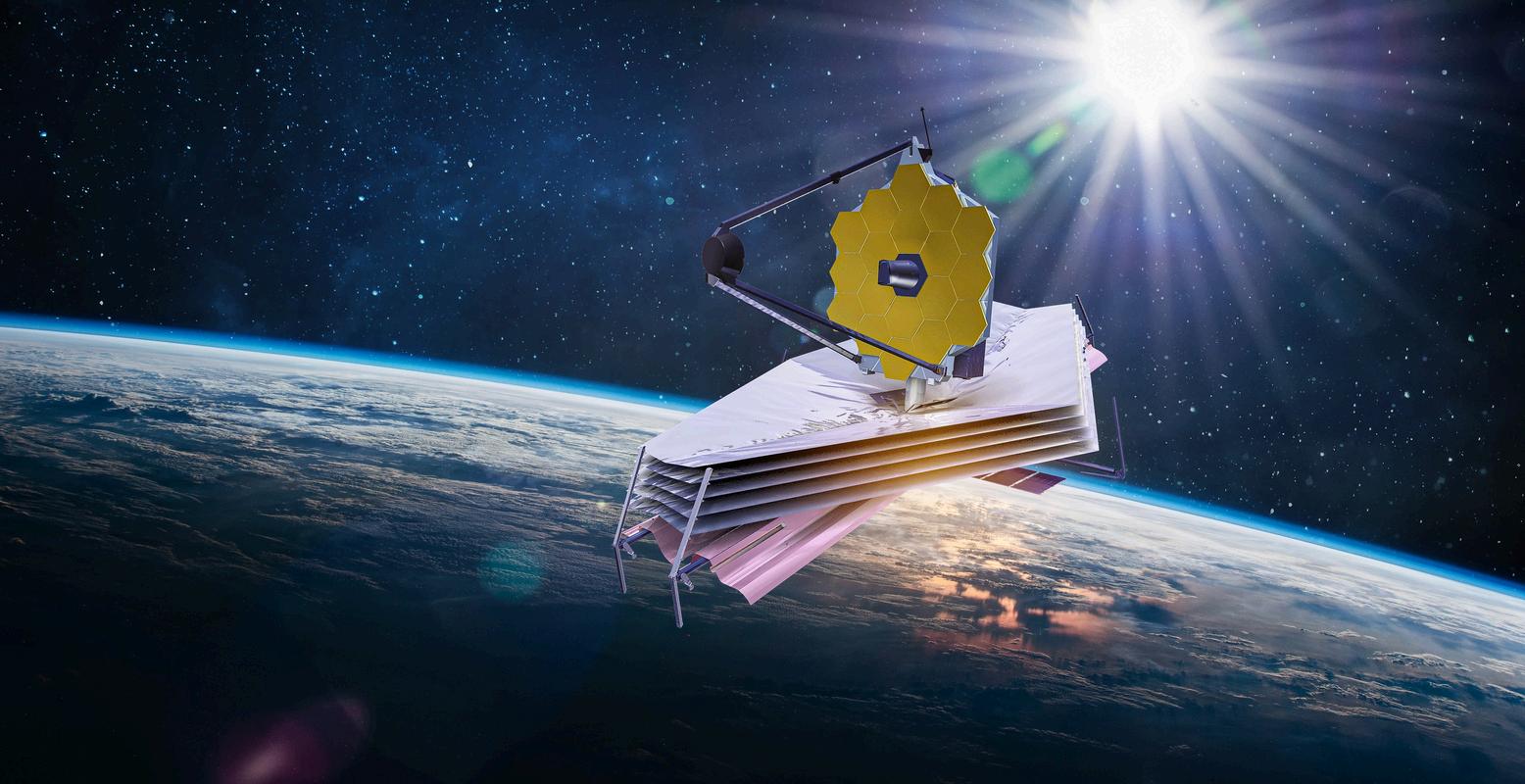
The James Webb Space Telescope was recently launched into space and features gold-coated beryllium mirrors for imaging infrared signatures of galaxies too distant for Hubble to witness. To detect faint infrared signals, the thermal signature of the telescope must be reduced and thermal radiation from other sources must be blocked. A sunshield was developed to protect Webb from external sources of radiation. The sunshield is composed of a Kapton substrate coated with aluminium and doped-silicon films to reflect incident radiation back into space. Spectroscopic Ellipsometry was used to ensure the film properties meet design specifications for critical components like the sunshield. Ellipsometry is also used to ensure that the optical properties of these specialised coatings enable the telescope to transmit beautiful images back to earth for many years to come.
Displays
Biomedical Devices
Medical devices implanted or adhered to the body require specialised coatings to ensure biocompatibility, improve functionality, and increase the lifespan of the device within the body Coatings are engineered to reduce inflammation caused by the device and therefore reduce the associated risk of infection. Thin-film coatings on these devices have also been designed to improve corrosion resistance caused by interactions with bodily fluids Many different methods of deposition have been developed to optimise the coatings.
Ellipsometry is one form of metrology used in development and quality control of thin-film deposition on bio-implanted or adhered devices Woollam technology is used to monitor the consistency of the coating as well as ensure its presence on the device
PURE ELECTRICAL INSULATORS ARE HIGHLY TRANSPARENT, BUT HIGHLY CONDUCTIVE METALS ARE OPAQUE. SO WHAT MATERIAL CAN BE USED THAT IS BOTH TRANSPARENT AND CONDUCTIVE? WE MUST FIND SUCH A MATERIAL TO MAKE OUR DISPLAYS AND TOUCHSCREENS WORK.
Indium tin oxide (ITO) is both transparent and conductive ITO optical properties vary a lot with deposition conditions and annealing, so monitoring the quality of the ITO and its thickness is important Ellipsometry is used for monitoring ITO film thickness and transparency at visible wavelengths while also being sensitive to absorptions in the ultraviolet, but it is very important for monitoring absorption in the infrared, which corresponds to the film’s electrical conductivity.
Improvements in display speed are critical for fast action in movies and sports Imagine a baseball, golf ball, or hockey puck leaving a comet tail behind on the screen because the display cannot refresh fast enough
Display pixel speed has been significantly enhanced using crystallised silicon films on the rear panel of the display Ellipsometry is used to monitor the thickness and crystallinity of these deposited polysilicon films
LCD displays used to be small, monochrome in color, and used in calculators, digital watches, etc Modern displays are full colour, extremely fast, and very large The coated films must be uniform over the entire panel size, and film uniformity has been a limiting factor in the size of displays for decades. With each new generation of larger displays, the film uniformity must be maintained An ellipsometer can fly over the large panels as they move on a production line to monitor film quality
SPECTROSCOPIC ELLIPSOMETRY
We will, of course, be running our Annual Spectroscopic Ellipsometry Workshops and CompleteEASE software course again in 2025.
WORKSHOP AND SHORT COURSE
In order to be among the first to know when and where, sign up to our mailing list. Or click on the link below to register your interest in attending with our Marketing and Business Support Manager, Angela Carslake...
We offer a wide range of spectroscopic ellipsometers, optimised for your particular application
The flexible ellipsometer VASE and VUV-VASE, based on a scanning monochromator is ideal for all kinds of R&D applications, covering the widest spectral range in the market from 140 to 4000 nm, or in combination with IR-VASE up to 30 µm Alternatively, our fast CCD based, rotating compensator spectroscopic ellipsometers M-2000 and RC2 are available for ex-situ as well as in-situ applications
Measure your Film Thickness and Optical Constants by
Ellipsometry
Since the 1960s, as ellipsometry developed to provide the sensitivity necessary to measure nanometer-scale layers used in microelectronics, interest in ellipsometry has grown steadily Today, the range of its applications has spread to the basic research in physical sciences, semiconductor and data storage solutions, flat panel display, communication, biosensor, and optical coating industries
What’s your application?
We love to hear about your scientific challenges So, to discuss ellipsometry and your application, contact our Technical Director, Dr. Shayz Ikram, by email below or call (01372) 378822
Email Angela
OPTICAL FILTERS FOR ASTRONOMY
Astrophotography uses spectral imaging to measure diverse properties
HARVARD STUDY REVEALS MARS MAY HAVE BEEN HABITABLE 4BN YEARS AGO
The Quantum Diamond Microscope (QDM) is a powerful tool for revealing the unknown Recently, a team at Harvard University used the QDM to provide new insights about Mars, including its habitability
Dr Jiahui Qi
The Sorby Centre for Electron Microscopy, School of Chemical Material and Biological Engineering, The University of Sheffield
Institution:
Tribology and Wear Lab, School of Chemical Materials and Biological Engineering, The University of Sheffield
Research Focus:
The Tribology and Wear Lab at the School of Chemical Materials and Biological Engineering, University of Sheffield, is recognised for its expertise in the high-resolution characterisation of microstructures, especially surfaces and interfaces The lab’s research programs, led by Professor Rainforth, cover a wide array of materials science fields, focusing on developing new, high-strength materials and understanding surface phenomena that occur during wear and
Key Research Areas: using
High-resolution Transmission Electron
Microscopy: The lab utilises this advanced technique to study atomic structures, particularly at interfaces found in nanoscale multilayer coatings and functional ceramics. This research is critical for improving the performance of materials in demanding environments
Tribocorrosion and Tribochemistry: A significant portion of the lab’s research is dedicated to understanding the dynamic microstructural changes that occur due to tribological contact, such as friction and wear, in both metallic and ceramic systems. The focus is on how these processes activate chemical or electrochemical reactions at the surfaces, leading to wear and corrosion in materials like hip arthroplasties and zirconia ceramics.
Wear and Friction in Biomedical Devices:
The lab extensively studies the performance of materials used in biomedical applications, h hi i l t f i h
Oxidation and Surface Degeneration
Phenomena: The lab also investigates oxidation during processes like hot rolling in metals and hydrothermal degradation of ceramics. Understanding these phenomena helps in designing new alloys that are more resistant to surface degradation
Microstructural Evolution During Metal Processing: Research is conducted on metals like titanium, magnesium, and steel to understand how their microstructures evolve during processing. The goal is to develop new materials with enhanced mechanical properties for industrial applications
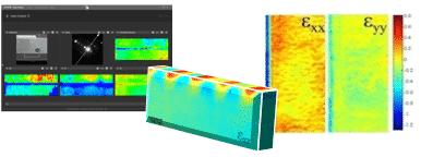
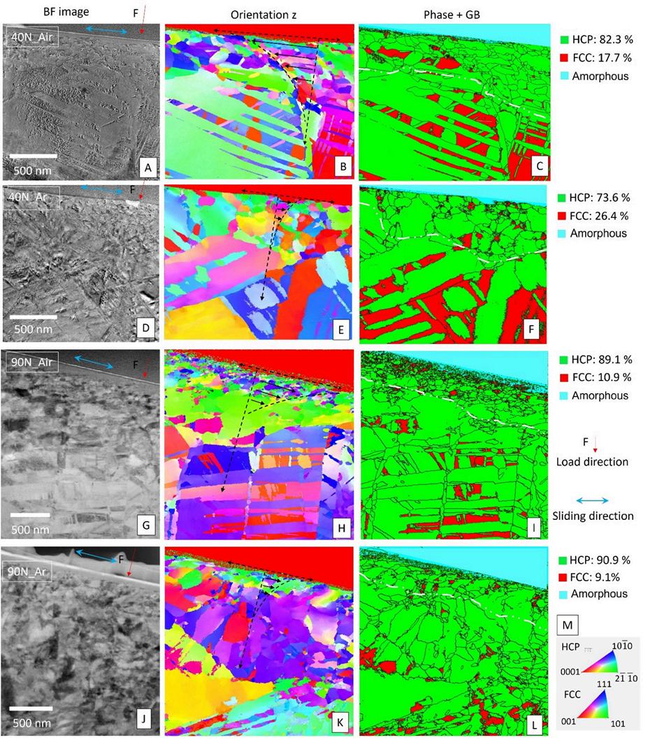
NanoMegas results for Ar and open-air samples under 40N (A to F) and 90N (G to L) load. The top and 3rd panels (A to C, and G to I, respectively) shows BF images and corresponding crystallographic z-orientation, and phase maps superimposed with grain boundary, for the open-air samples. The 2nd and 4th panels (D to F, and J to L, respectively) presents the same maps for the Ar samples The colour keys for z-orientation maps are provided (M). The percentage fractions of measured phases are presented next to the phase maps (C, F, I and L), where green is HCP, red is FCC and cyan is amorphous The blue double arrows indicate the sliding direction and surface position, while the red arrows represent the applied load direction Schematic drawings in B, E, H and K illustrate the strain distribution from the surface to the bulk material.
(Qi, J , et al “Tribocorrosion behaviour of CoCrMo in simulated body fluid under anaerobic conditions.” Wear 556 (2024): 205523.)
Challenges Before NanoMEGAS
Prior to acquiring the NanoMEGAS system, the lab encountered limitations in quantitatively interpreting the nanoscale structural changes that occurred during tribological processes. While conventional methods like transmission electron microscopy (TEM) and electron backscatter diffraction (EBSD) offered some insight, they could not fully resolve the fine details of highly deformed structures at the nano-level Specifically, the team struggled to quantify dislocation densities and detect subtle phase transformations that influence friction and wear This lack of precision inhibited their ability to predict and improve material performance, particularly for biomedical implants where understanding the interplay between wear, corrosion, and protein interaction is crucial.
Why NanoMEGAS
Precession Electron Diffraction (PED):
NanoMEGAS provided a breakthrough with its precession electron diffraction technology, offering spatial resolution between 0 5–5 nm and an angular resolution of approximately 0.1°. This capability allowed the lab to analyse the ultrafine, nanocrystalline structures formed under severe tribological conditions, which were previously very challenging using conventional techniques.
Resolution of Complex Structures: The ultrafine grain structures that develop in materials like Ti-6Al-4V and CoCrMo during tribocorrosion were difficult to characterise using traditional methods PED allowed the lab to accurately index different phases and calculate dislocation densities, providing a more comprehensive understanding of the deformation mechanisms at play.
The microstructure modification under different tribo-corrosion conditions (Qi, J , et al “Insights into tribofilm formation on Ti-6V-4Al in a bioactive environment: Correlation between surface modification and micro-mechanical properties.” Acta Biomaterialia 141 (2022): 466-480.)
ASTAR Software Integration:
NanoMEGAS’s ASTAR software enabled automated phase and orientation mapping, which was crucial for the lab to interpret the highly deformed structures efficiently. This software allowed the lab to correlate the nanoscale structural data with the wear performance of materials.
Ability to Quantify GND Density:
NanoMEGAS’s capabilities to obtain data are then used for calculating the geometrically necessary dislocation (GND) density This helped the lab evaluate the degree of deformation in different phases and under various tribological conditions. This allowed for more precise predictions regarding how materials will perform under wear and corrosion.
How NanoMEGAS Changed the Research
The microstructure modification under different tribo-corrosion conditions. (Qi, J., et al. “Insights into tribofilm formation on Ti-6V-4Al in a bioactive environment: Correlation between surface modification and micro-mechanical properties ” Acta Biomaterialia 141 (2022): 466-480.)
Results and Key Findings
In one of the lab’s key research projects, NanoMEGAS played a vital role in understanding the microstructural evolution of Ti-6Al-4V and CoCrMo alloys during tribocorrosion tests conducted in a simulated body fluid environment. Tribocorrosion an interaction between wear, friction, and electrochemical corrosion has a significant impact on the performance of biomedical implants
Using NanoMEGAS, the lab team was able to quantitatively measure the geometrically necessary dislocation (GND) density and characterise the formation of tribofilms The ability to measure deformation structures quantitatively at nanoscale precision was critical to uncovering how these tribofilms influence material wear resistance.
NanoMEGAS enabled the team to achieve several key results that were unattainable with conventional techniques: Quantified GND density and identified nanostructural changes under different tribocorrosion conditions. Detected the formation of a protective tribofilm that reduced friction and wear, particularly under conditions with a positive potential and protein interaction.
PED images from cross-sections of the worn surface. Orientation, GB and phase maps of 30N (A, B and C), 45N (D, E and F) and 50N (G, H and I) samples, respectively
Black arrows indicate sliding direction and the surface position The colour keys indicate the phases and the orientation in hcp and fcc systems (Qi, J., et al. “Investigation of the wear transition in CoCrMo alloys after heat treatment to produce
User Experience and Support
Although the initial use of NanoMEGAS began without in-person training due to the COVID-19 pandemic, the lab was later able to reconnect with the NanoMEGAS support team for training and updates. The hands-on support significantly enhanced the team’s understanding of the system, allowing them to expand its application to more complex projects The training helped ease the challenges of data processing and interpretation, leading to more efficient use of the system
Grain boundary (GB) superimposed on the geometrically necessary dislocation (GND) density distribution maps in the subsurface regions from the four selected testing conditions The scale bar is 100 nm on the PBS sample and is 500 nm for the remaining three samples The colour scale is log(GND density in m2) Arrows indicate the sliding direction and surface position.
(Qi, J., et al. “Insights into tribofilm formation on Ti-6V-4Al in a bioactive environment: Correlation between surface modification and micromechanical properties.” Acta Biomaterialia 141 (2022): 466-480 )
Impact and Future Opportunities
NanoMEGAS has been transformative in enabling the Tribology and Wear Lab to conduct advanced research at the University of Sheffield. The lab is now exploring new research avenues, including in situ heating experiments in TEM to observe phase transformations in real time. The data gathered using NanoMEGAS will further contribute to the lab’s ongoing research into wear-resistant materials and their application in biomedical and industrial sectors.
The lab is also enthusiastic about collaborating with other institutions and industrial partners through the Henry Royce Institute at Sheffield,
Listofpublications: 1) Qi J, Cole T, Foster A & Rainforth WM (2024) Tribocorrosion behaviour of CoCrMo in simulated body fluid under anaerobic conditions. Wear, 556-557, 205523-205523. 2) Qi J, Ma L, Gong P & Rainforth WM (2023) Investigation of the wear transition in CoCrMo alloys after heat treatment to produce an HCP structure. Wear, 518-519, 204649204649. 3) Qi J, Guan D, Nutter J, Wang B & Rainforth WM (2022) Insights into tribofilm formation on Ti-6V-4Al in a bioactive environment: Correlation between surface modification and micro-mechanical properties. Acta Biomaterialia, 141, 466-480. 4) Xu Y, Qi J, Nutter J, Sharp J, Bai M, Ma L & Rainforth WM (2021) Correlation between the formation of tribofilm and repassivation in biomedical titanium alloys during tribocorrosion. Tribology International, 163, 107147-107147. 5) Namus R, Nutter J, Qi J & Rainforth WM (2021) Sliding speed influence on the tribocorrosion behaviour of Ti6Al4V alloy in simulated body fluid. Tribology International, 160, 107023-107023.
offering access to NanoMEGAS through the university’s Equipment Access Scheme
NanoMEGAS has been transformative in enabling the Tribology and Wear Lab to conduct advanced research at the University of Sheffield. The lab is now exploring new research avenues, including in situ heating experiments in TEM to observe phase transformations in real time.
The data gathered using NanoMEGAS will further contribute to the lab’s ongoing research into wear-resistant materials and their application in biomedical and industrial sectors The team is keen to host future workshops to share knowledge and promote the system’s capabilities to the broader research community.
Conclusion
NanoMEGAS has proven to be an indispensable tool in advancing our understanding of tribological processes at the nanoscale. Its ability to precisely characterise microstructural changes has provided invaluable insights into material performance in a wide range of applications.
For more information or collaboration inquiries, please contact the Sorby Centre for Electron Microscopy at i.ross@sheffield.ac.uk or visit The University of Sheffield Electron Microscopy Facility
Agriculture is a vital sector of the UK economy, using 69% of the country’s land, employing 1% of its workforce, and contributing 6.2% of the national Gross Value Added (GVA) in 2021. The UK produces around 54% of its own food, and the sector also provides export opportunities that support rural communities.*
*source
It is vital that the industry is supported by new developments, and has access to the latest technology to drive it forward Quantum Design UK and Ireland offers a number of solutions to the challenges faced by the agricultural sector. A broad range of applications, using the very latest imaging cameras from our principals –Specim Hyperspectral, Raptor Photonics and InfraTec thermographic cameras
Working in collaboration with our worldwide service colleagues we offer:
System installations and user training
Spare parts and accessories
System calibrations
Instrument relocation assistance
Test and sample measurements, from either our Darmstadt or San Diego applications laboratories
Ongoing system support
Dr. Jordan Thompson, Service Manager
Jordan received his PhD in 2016 from the University of Oxford on the topic of inelastic neutron scattering and heat capacity measurements on rare earth oxide materials at low temperatures and high magnetic fields. Jordan joined Quantum Design UK and Ireland in 2017, and his specialties lie in making Quantum Design equipment work for customers; through installing new equipment, servicing existing equipment, and advising customers on how to optimise their experiments to get the best possible results.
The QDUKI service team have provided professional, responsive, and thorough support over many years. Their efficient assistance has been vital in keeping our MPMS and PPMS in good working order. This has allowed our research group to publish numerous academic papers relating to material discovery and characterisation.”
Dr Hongjun Niu, University of Liverpool
Liam Colman, Field Service Engineer
Liam graduated with a first-class master's degree in 2021 from the University of Lancaster, with a specialisation in low temperature helium physics He operated their advanced wet dilution refrigerator at a base temperature of 2mK to study quantum turbulence in superfluid He-3. Liam joined Quantum Design in January 2024. He assists customers with installation or operation of their systems to ensure their experiments run as smoothly as possible Liam specialises in dealing with Montana Instruments.
The UK is making progress towards using more renewable energy to reduce its carbon emissions and reach net zero by 2050. There are ambitious targets set for all aspects of environmental concerns, including recycling, emissions reduction, species abundance and water health.
The climate challenge faces citizens, scientists, industry, and governments alike
From recycling and renewable energy to waste and environmental management, our customers are looking at new and innovative ways to meet these challenges Researchers and scientists need to be aware of new developments, and have access to the latest technology, to reach these goals QDUKI offers solutions to advance research with highly sensitive measurement instrumentation
FOCUSON:
The HR Series is a line of high-reliability cryogenic temperature sensors for mission-critical applications. Starting with Lake Shore’s proven temperature sensor technology, we have developed a family of offthe-shelf sensors that have already undergone extreme testing steps to assure you of extra reliability.
FOR WHEN THE BEST NEEDS TO BE BETTER
In situations where cryogenic temperature control or monitoring forms a critical component of a system and the cost of sensor failure far exceeds the cost of the sensor, subjecting sensors to a higher level of scrutiny becomes vital Projects where outcomes are worth far more than the sum of their parts are prime examples of this and include:
Space telescopes
Supercolliders
Fusion reactors
Research satellites
Maglev locomotives
REDUCE RISK ON CRITICAL PROJECTS
On time
Following standardised testing procedures, these sensors are built on regular production schedules and stocked for rapid delivery, resulting in lead times comparable to standard commercial sensors. Predefined testing protocol also cuts paperwork no need to define different detailed sensor requirements for every program
On budget
Traditionally, sensor procurement for critical programs required that additional sensors for destructive qualification tests be purchased for each lot, increasing the total cost of the project without increasing the number of sensors that are available to install. HR sensors are different Lake Shore performs the qualification testing for each lot, with the resulting screening and qualification test report being supplied to sensor buyers at no additional cost With HR sensors, you only pay for the sensors that you use
APP NOTE: Cernox™ Resistance Temperature Sensors for High Energy Physics Applications
The cryogenic temperature sensing requirements of superconducting magnets used in high energy physics accelerators present a unique challenge The sensors must operate at cryogenic temperatures below 4.2 K with low magnetic field-induced calibration offsets at fields ranging to 10 T. They must provide high resolution with fast response times to detect potential superconducting magnet quenches
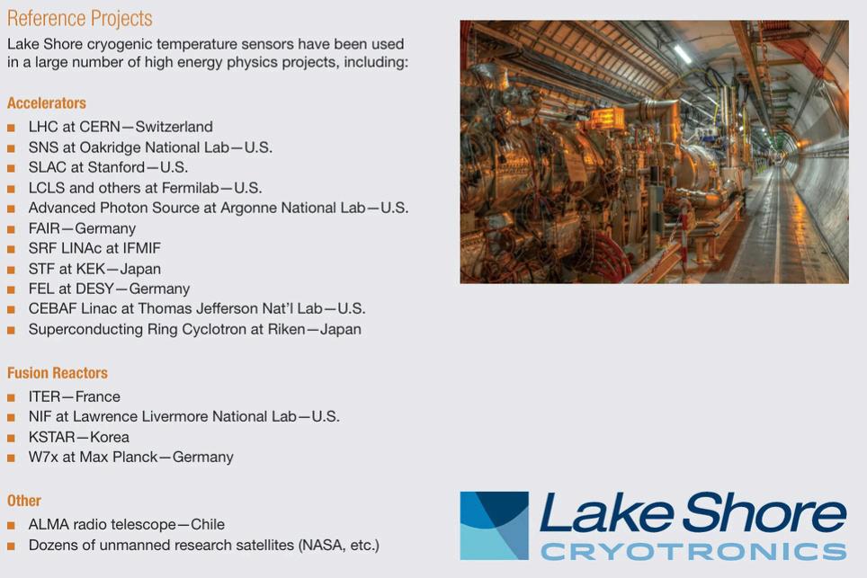
ReferenceProjects
Lake Shore cryogenic temperature sensors have been used in a large number of high energyphysicsprojects,including:
Accelerators
LHCatCERN,Switzerland
SNSatOakridgeNationalLab,USA
SLACatStanford,USA
LCLSandothersatFermilab,USA
AdvancedPhotonSourceatArgonne NationalLab,USA
FAIR,Germany
SRFLINAxatIFMIF
STFatKEK,Japan
FELatDESY,Germany
CEBAFLinacatThomasJefferson NationalLab,USA
SuperconductingRingCyclotronat Riken,Japan
The sensors must be stable over time and thermal cycling with low radiation-induced calibration offsets up the anticipated accumulated dose over the lifetime of the accelerator. This combination of unique requirements severely limits temperature sensor choices for monitoring superconducting magnets.
Cernox™ resistance temperature sensors, manufactured by Lake Shore Cryotronics, Inc , were specifically designed and developed for the purpose of monitoring superconducting magnets used in high energy accelerator facilities and meet the criteria required for this application This work details performance specifications for Cernox resistance temperature sensors with regard to their suitability for high energy physics applications.
FusionReactors
ITER,France
NIFatLawrenceLivermoreNational Lab,USA
KSTAR,Korea
W7xatMaxPlanck,Germany
Other
ALMAradiotelescope,Chile
Dozensofunmannedresearch satellites(NASAetc)
The UK is a global leader in semiconductor chip design. The country will play a key role in developing the industry in the future. QDUKI is ready to assist with the challenges we will face while shaping the development of advanced packing and compound semiconductors.
We have continually added to our product portfolio by acting as distributor for other market leaders who provide solutions for semiconductors, including J A Woollam, InfraTec, Sigray, 4D Technology and Lake Shore Cryotronics This means we can provide our customers with the right solutions for their semiconductor applications.
Our Other Magazines
Free to read
1
CRYOGENICS
MATERIAL CHARACTERISATION AT LOW TEMPERATURE
Our two cryogenics magazines, featuring updates on new cryogenic products, publications, and white papers related to our offerings. Plus an interview with Prof. Jason Robinson. Quantum Design is heavily involved in education and in this edition we explore various global initiatives from QD.
read ed 2 now read ed 1 now
IMAGING CAMERAS 2
THERMOGRAPHY, HIGH SPEED, SWIR, CCD AND XRAY CAMERAS
The second edition of the QDUKI Imaging Cameras magazine, featuring case studies on “Thermography: On The Trail of the Fault” and “Detecting Foreign Objects on Food with Hyperspectral”. Plus more applications, new products and solutions to your scientific challenges.
3 QUANTUM
CRYOGENICS FOR QUANTUM
In this inaugural issue of our Quantum Magazine, we showcase the systems, solutions, and strategic initiatives that position our company at the forefront of the quantum revolution. Explore compelling case studies, insightful interviews, and valuable information as we embrace the future of quantum technology.
AGRICULTURE
AGRICULTURAL APPLICATIONS
Agriculture has seen a large growth in investment for research and development in recent years, and we have endeavoured to help our customers implement new techniques Precision farming, plant research, quality assurance, and animal husbandry are key topics featured in this magazine.
SPACE
EDITIONS 1 AND 2
Quantum Design UK and Ireland brings you the latest in space and aerospace flight qualified testing and components Our suppliers are responsible for supporting the development of iconic inventions such as the James Webb Space Telescope and the Mars Perseverance Rover. Including - Imaging Venus, Meteorite Analysis; Space Camera Solutions; Space Instrument Failure Analysis and much more
This magazine delves into solutions for non-destructive testing challenges in applications from automated manufacture to aerospace. Featuring case studies, applications,
ENVIRONMENT
RECYCLING, RENEWABLE ENERGY SOURCES AND MORE
Researchers and scientists need to be aware of new developments, and have access to the latest technology, to reach these goals. Semiconductors, for instance, are essential for the transition to renewable energy and the electricity grid by enabling the conversion, storage, and distribution of energy from renewable sources QDUKI offers solutions to advance research with highly sensitive measurement instrumentation.
read now
SEMICONDUCTORS
HIGH-TECH INSTRUMENTATION FOR SEMICONDUCTORS
Semiconductors underpin the ambition to advance quantum, telecom, and AI technologies. QDUKI are proud to be part of that development, strengthening the position through new and innovative solutions. This magazine features a new camera for PET semiconductor inspection, semiconductor device analysis using AFM, and a case study on the structure of magnetic semiconductors.
read now
Imaging Cameras
Thermal imaging cameras
Hyperspectral imaging cameras
SWIR cameras
CCD and EMCCD cameras
X-ray cameras
CMOS cameras
High-speed imaging cameras
We have teamed up with the world leaders in each specialism to provide a extensive range of imaging cameras, including Specim, Cordin, InfraTec and Raptor Photonics. We welcome the opportunity to discuss your requirements in further details.
Quantum Design UK and Ireland are really pleased to be able to offer three incredible Specim Hyperspectral Imaging Cameras and the ImageIR 8300 from InfraTec to researchers.
Quantum Design selected six exceptional individuals from around the world, offering them a unique opportunity to delve into a week of intensive, advanced measurement training. Utilising our stateof-the-art PPMS®, MPMS®3 and FusionScope® platforms, our Applications Scientists, Randy Dumas and Darius Choksy, are dedicated to transforming participants into superusers This initiative underscores our commitment to fostering the next generation of scientific talent and enhancing their proficiency with cuttingedge technologies
New to the instrument lineup for the Winter School is FusionScope®. Students were asked to bring samples for measurements that would benefit from equipment they do not have at their home institutions, and the FusionScope is generating a lot of interest When combined with our standard suite of measurement techniques, the unique correlative microscopy measurements enabled by the FusionScope provide a comprehensive and complete examination of a wide range of materials and devices.
New This Year
This year at the Winter School, we were lucky enough to have on hand the iQuantum Helium-3 for the MPSM®3. The iQuantum Helium-3 enables measurements of the DC and AC magnetic moment below 0.5 K. Kyle Kirkpatrick is demonstrating the basic functionality and helping to prepare a measurement for one of the students
UK attendee reviews the inaugral winter school
JUST SIX exceptional users of QD’s PPMS and MPMS 3 platforms from around the world were offered a unique opportunity to experience a week of intensive, advanced measurement training “
Last year marked the first ever QD Winter School, led by application scientists Randy Dumas and Darius Choksy, and held at QD Headquarters in San Diego The theme was to transform users into superusers The initiative underscores QD’s commitment to fostering the next generation of scientific talent and enhancing their proficiency with cutting-edge technologies.
One of those lucky enough to be invited was Sivaloganathan Kumaran, a PhD Candidate in Connected Electronic and Photonic Systems at Sidney Sussex College, University of Cambridge.
Attending the Quantum Design Winter School 2024 was an invaluable experience that significantly enriched my practical understanding of experimental quantum physics…
The itinerary was meticulously planned to cover a broad spectrum of topics, offering a mix of theoretical presentations, handson demonstrations in the Apps Lab, and, most importantly, time to conduct experiments on research-relevant material samples and devices
“Each day started with a deep dive into the intricacies of quantum physics experiments, followed by comprehensive sessions on the MPMS3 and DynaCool, a look into the design of FusionScope and OptiCool, and more tailored measurements on attendees’ own samples. What set this Winter School apart from the summer schools I have attended was its handson focus, rather than the usual ‘death by PowerPoint’ approach.
The opportunity to engage directly with cuttingedge technology and conduct measurements under the guidance of experts was invaluable, with participants instructed to bring their most difficult samples to get direct feedback on improving their experiments and gather data for their research This combination not only solidified my theoretical knowledge but also enhanced my practical skills, making me aware of various techniques and their applications.
IN SUMMARY, THE WINTER SCHOOL WAS ONE OF THE MOST VALUABLE EXPERIENCES OF MY PHD TO DATE. I HIGHLY RECOMMEND IT TO ANYONE LOOKING TO BROADEN THEIR UNDERSTANDING AND PRACTICAL RESEARCH SKILLS”
This weeklong winter school is geared towards lab managers and graduate students in the second half of their PhD and will provide advanced training on both the PPMS (including DynaCool and VersaLab) and MPMS3 platforms. Specific measurement options discussed will be tailored to the needs and interests of attending students, who are encouraged to bring samples. QD provides room and board for the week, as well as social excursions.”
Want to go next year?
Application deadline Nov 2025
Awardees notified by December
To apply, email a CV along with a statement describing how measurement equipment offered by Quantum Design is a critical part of your research and how you would benefit from attendance to apps@qdusa.com
Airfare and travel to San Diego will be the responsibility of the attending student.
Sivaloganathan Kumaran, University of Cambridge.
H A V E Y O U R S A Y
SEND IN YOUR RESEARCH OR WHITE PAPERS
We'd love to share your findings
SHARE YOUR APPLICATIONS
Wh t h b i
QDUKI STUDENTS
Want to share what you are currently working on ?
QD want to hear from you! If you want to promote your research