(Online)
International Research Journal of Engineering and Technology (IRJET)
e-ISSN: 2395-0056
Volume: 07 Issue: 04 | Apr 2020
p-ISSN: 2395-0072
www.irjet.net
High Frequency Tri-band Patch Antenna with Enhanced Bandwidth Anjali K Netke1, V. V. Yerigeri2 1,2Department
of Post Graduation, MBES COE Ambajogai (MS), India 1,2Dr. B. A. T. U. Lonere, India 2Professor & Head of Department, MBES COE, Ambajogai (MS), India ---------------------------------------------------------------------***----------------------------------------------------------------------
Abstract
We demonstrated and presented triple band line fed microstrip patch antenna for wireless communication application. In proposed design, we introduced F-shape patch and ground plane of antenna, to enhance the bandwidth of mictrostrip antenna. Adjusting the dimension of ground plane and patch, its enhanced bandwidth at primary and secondary resonance mode can increased sufficiently to achieve desired bandwidth of proposed antenna. We demonstrated many antenna structures to study of these parameters on the resulting tri band response. In this paper, we designed tripple-band microstrip rectangle antenna with slot antenna using line-feed technique, it support the three wireless communication bands that is (12.9-14.3 GHz), (18.2-19.8 GHz) and (20.8-23.8 GHz). Key Words: Trippleband Microstrip antenna, bandwidth enhancement, Co-axial feed technique.
2. PROPOSED DESIGN
1. INTRODUCTION With development of wireless communication and microstrip antenna it has been found that, Microstrip antenna analysis with different feed technique like co-axial, line-feed technique etc, is good candidate t improve antenna performance. Microstrip patch Antenna experimentally optimize antenna parameters and decreases the Return Loss up to -35dB for the frequency range to operate for Bluetooth antenna in frequency range 2.4 GHz to 2.5GHz and VSWR is less than 1.5 by using RT DUROID 5880[1]. In further study of optimization of dual band microstrip antenna [2] it has been found that the return loss for dual band Frequency at 2.4GHz is -43dB and at 3GHz is -27dB and acceptable VSWR. To get compact size and maintain performance of antenna for multiple band that is dual band, triple band antenna etc., various shapes of antenna was integrated [3]. It was presented in [4], introducing slot into patch that is L-Shape, experimentally increase bandwidth up to 13%. To enhance bandwidth further various shapes like L-shape, U-shape etc., slot was introduced and bandwidth up to 42% was increased [5,6]. In [7] and [8] the author’s proposed bandwidth enhancement techniques that is by using photonic band gap structure and wideband stacked microstrip antennas respectively. By introducing stacked microstrip antenna band width and gain was enhanced. While Designing of symmetrical microstrip antenna, it has been found that microstrip antenna has narrow Bandwidth [9], Asymmetrical © 2020, IRJET
|
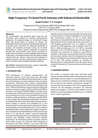
position of patch antenna on ground affect the performance of antenna that is to enhance bandwidth it was also found that asymmetrical position of slot on patch affects performance of antenna[10] that is asymmetrical L-shape, Ushape position of slot on patch affects the performance. In [10] designed asymmetrical slot of L-shaped on patch antenna for UWB application with acceptable return loss that is -10dB and peak gain 2.2 to 6.1 dBi for operating bandwidth 3.01-11.30 GHz frequencies. In this paper we simulated and presented our design by using HFSS.13 simulator. In this paper a line feed patch with two rectangle slot microstrip antenna with two antisymmetrical notch (Figure 1) is designed and simulated for the frequency range of 1-5 GHz. This antenna presents an extension to Miniaturization of Differentially-Driven Microstrip Planar Inverted F Antenna [11]. The proposed antenna has a gain of 1.7 dBi.
Impact Factor value: 7.34
|
The results of proposed triple band microstrip patch antenna verified in HFSS Simulator with optimization. Actual patch shape is shown in figure 1, it consists of symmetrical Fshape structure on both side of dielectric substrate. On patch side and ground side parasitic symmetrical rectangle are introduced (as shown in figure 1 & 2). The resulting antenna structure has the following parameters; the dielectric substrate has length L = 18.4 mm, and its width W =13 mm, dielectric constant and height of substrate are εr = 4.4 (FR-4) and h= 1.0mm respectively.
Figure 1: Proposed antenna design (Patch)
ISO 9001:2008 Certified Journal
|
Page 1572