International Research Journal of Engineering and Technology (IRJET)
e-ISSN: 2395-0056
Volume: 06 Issue: 05 | May 2019
p-ISSN: 2395-0072
www.irjet.net
DESIGN AND IMPLEMENTATION OF HIGH SPEED FPGA CONFIGURATION USING SBI Mr. B.GOWRI SHANKAR1, V.J.JAYAPARKAVI2 1Assistant
Professor, Department of Electronics and Communication Engineering, Sri Ramanujar Engineering College, Chennai.
2Department
of Electronics and Communication Engineering, Sri Ramanujar Engineering College, Chennai
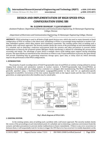
----------------------------------------------------------------***--------------------------------------------------------------ABSTRACT:- FPGA technology is used in all kinds of high speed devices now, which also need so many demands in Quick configuration of FPGA at runtime is the latest need. Scheduling in FPGAs is increasingly being employed in modern realtime embedded systems, which often impose strict timeliness constraints. The existing system aims at tackling such a problem with a self aware approach. The security module checks the course of the proceedings at each intermittent point of a schedule and on detecting a malicious environment heals the scenario and takes precautions to prevent similar malfunctions in future.In the proposed system SBI(Spare blocks interfacing) is utilized for scheduling the process more accurately and timely. The advantage of spare block is multiple choice multi tasking spare support during scheduling process. The spare blocks are interfaced in four directions so if there is any Trojan malfunction in process, the spare blocks will provide scheduling help by generating temporary storage space, spare data, or delay clock etc which obviously improve the performance of the FPGA configurations. 1. INTRODUCTION The property of quick reconfiguration of Field Programmable Gate Array(FPGA) at runtime is being utilized in arenas ranging from avionics and automotive systems to nuclear reactors. A Field-Programmable Gate Array(FPGA)is an integrated circuit designed to be configured by a customer or a designer after manufacturing. The FPGA configuration is generally specified using a Hardware-Description Language(HDL),similar to that used for an application-specific integrated circuit(ASIC). Correctness of the time system depends both on the logical results and the time of the result generation, as output generation after deadline may be catastrophic.
Fig 1. Block diagram of FPGA CLB’s 2. EXISTING SYSTEM: In the existing system, aims at tackling such a problem with a self aware approach. The security module checks the course of the proceedings at each intermittent point of a schedule and on detecting a malicious environment heals the scenario and takes precautions to prevent similar malfunctions in future immediately. If there is any error occurrence in between them, it will sequentially wait for its time to trigger the CPU that error has occurred. It is totally dependent on the
Š 2019, IRJET
|
Impact Factor value: 7.211
|
ISO 9001:2008 Certified Journal
|
Page 2034