International Research Journal of Engineering and Technology (IRJET)
e-ISSN: 2395-0056
Volume: 06 Issue: 02 | Feb 2019
p-ISSN: 2395-0072
www.irjet.net
Physical Design Implementation of Single Core 32 Bit RISC Processor on 28nm Technology Feroz Ahmed Choudhary1, Amay Shiva Naik2, Dr. Rajashekhar C Biradar3 1,2,3Dept.
of Electronics and communication Engineering, REVA University, Bengaluru, India ----------------------------------------------------------------------***---------------------------------------------------------------------
Abstract – Physical Design implementation means the
rule checking). At last we perceive Graphic Database System (GDS II) file, it is database file format which is industry standard for data substitute of IC layout artwork. It is binary file representing planar geometric shapes, text labels and other information about layout in hierarchical form.
layout assembling and connectivity of digital logic gates as per the design input file (called as netlist) of an Integrated chip say a processor, by meeting the design specifications like timing, power and area. Here in this design we have used the inputs given by the synthesis team and further physical design flow has been carried out in a proper physical design flow i.e. from import design, floor plan further placement till signoff using the Physical design tools. At each stage checks are done such as timing (hold & setup), quality of report, congestion, routing etc. Key Words: Import Design, Floor Plan, Placement, Place opt, Clock Tree Synthesis, Opt Clock Tree Synthesis, Routing, opt Routing, Signoff.
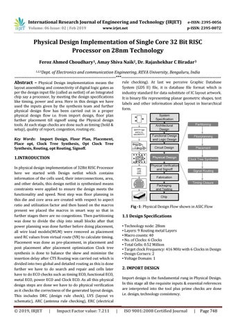
1.INTRODUCTION In physical design implementation of 32Bit RISC Processor here we started with Design netlist which contains information of the cells used, their interconnections, area, and other details, this design netlist is synthesized means constraints were applied to ensure the design meets the functionality and speed. Next step was floor planning in this die and core area are created with respect to aspect ratio and utilization factor and then based on the macros present we placed the macros in smart way so that in further stages there are no congestions. Then partitioning was done to divide the chip into small blocks after that power planning was done further before doing placement, all wire load models(WLM) were removed as placement used RC values from virtual route (VR) to calculate timing. Placement was done as pre-placement, in placement and post placement after placement optimization Clock tree synthesis is done to balance the skew and minimize the insertion delay after CTS Routing was carried out which is divided into two global and detailed routing as this is done further we have to do search and repair and cells later have to do ECO checks such as timing ECO, functional ECO, metal ECO, power ECO and Clock ECO. As all this physical design steps are done we have to do physical verification as it checks the correctness of the generated layout design. This includes DRC (design rule check), LVS (layout vs schematic), ARC (antenna rule checking), ERC (electrical
© 2019, IRJET
|
Impact Factor value: 7.211
Fig -1: Physical Design Flow shown in ASIC Flow
1.1 Design Specifications ▪ Technology node: 28nm ▪ Layers: 9 Routing metal Layers ▪ Macro counts: 40 ▪ No. of Clocks: 6 Clocks ▪ Total Cells: 0.52 Million ▪ Target clock Frequency: 416 MHz with 6 Clocks in Design ▪ Design Corners: 2 ▪ Voltage Domain: 1
2. IMPORT DESIGN Import design is the fundamental rung in Physical Design. In this stage all the requisite inputs & essential references are interpreted into the tool plus prime checks are done i.e. design, technology consistency.
|
ISO 9001:2008 Certified Journal
|
Page 748