International Research Journal of Engineering and Technology (IRJET) Volume: 03 Issue: 07 | July-2016
www.irjet.net
e-ISSN: 2395 -0056 p-ISSN: 2395-0072
FORMAL PROPERTY VERIFICATION OF COUNTER FSM AND I2C SNEHA S1, ROOPA G2 1
PG Student, Dept. of Electronics and Communication Engineering, Nagarjuna College of Engineering, Bengaluru Karnataka Email: sneha44enz@gmail.com 2 Assistant professor, Dept. of Electronics and Communication Engineering, Nagarjuna College of Engineering, Bengaluru, Karnataka Email: roopa.gurijepalli@gmail.com
---------------------------------------------------------------------***---------------------------------------------------------------------
Abstract - In the present days, due to the increased
complexity of multimillion gates such as complex SOC, ASICs and DSP processors need to be verified effectively. About 70% of the VLSI design efforts to consumer verification. Some of the front end technologies are RTL functional verification, test bench verification coverage techniques, etc. are very difficult to design closure. These may not cover all the corner cases. By considering the above concerns, formal verification has become more important to verify the complex circuits and protocols. Model checking verifies temporal logic in formal verification. One can check the perfections of circuits or designs using HDL’s. Verification Interacting with Synthesis (VIS) is a tool. The tool is to implement model checking properties on up-counter and I2C protocols.
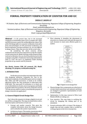
Floor planning: It identifies the placements of structures in a system and it allocates the space for each structure to meet some effective goals in a system.
Key Words: Counter FSM, I2C protocol, VIS, Model checking, CTL property verification using VIS
1. INTRODUCTION Verification process plays very important role in the chip designing industries, companies etc. Due to the increased complexity of multimillion gates such as complex SOC, ASICs and DSP processors, it needs to be verified effectively before the chip production in fabrication labs (FAB labs). The main goal of verification is to check and correct the defects in circuits, errors in programs and finally to get the defect free products. The term verification means “It is the process which is used to reveal that the purpose of design is stored in its application”.
Fig-1: Digital circuit design flow
Physical design: Here components are in the form of circuits (interconnections and systems) and those are changed to geometric representation of each circuit of design.
1.1 General Digital Circuit Design Flow
Optimization: In this step removal of Wire Load Models (WLM) are taking care.
Fig-1 shows the sequence to design a digital circuit and we call this as design flow. The steps are listed below with a brief description and function of each. [2]
Scan insertion: This step helps in verifying the circuit by designing the testing part or by simulation.
Concept and market research: This gives the complete information about the design structure and it embodies the system requirements.
Formal verification (RTL v/s Gates): The design of simple chip and also complex chip is verified by writing program in the form of properties.
Architectural specs: This mainly concentrates about the elements and components of the system.
© 2016, IRJET
|
Impact Factor value: 4.45
|
ISO 9001:2008 Certified Journal
|
Page 1326