
2 • 2025


2 • 2025

REDEFINING TIMING


OPEN SOURCE IS NOT FREE
EEPROM STILL GOING STRONG
AN EMBEDDED SYSTEM IS A LAYERED CHAOS
FINNISH COMPANIES HEADING FOR LATVIA

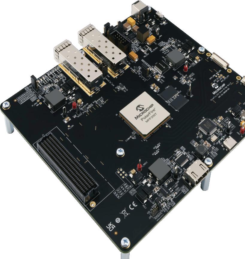
PolarFire®FPGAEthernetSensorBridgeforNVIDIA®HoloscandeliversflexibleintegrationforAI-driven sensorprocessingfromedgetocloud.Thissolutionsupportsmultipleprotocols,powerefficiency,security andreliabilityinoneseamlesspackage.NVIDIAapprovesthissolutionforuseinitspopularHoloscan ecosystem.
KeyFeatures
• Power-efficientprotocolconversion
• Highlysecure
• Singleeventupset(SEU)immuneforhighreliability
YoucanconfidentlychoosethePolarFireFPGAEthernetSensorBridgeforNVIDIAHoloscan, acomprehensivesolutionrenownedforitstechnicalexcellenceandcustomer-centricdesign.



Will AI be the end of coding?
AWS now envisions a future where hand-written code becomes the exception rather than the rule. Generative AI agents are evolving from simple autocomplete tools into autonomous collaborators that design architectures, generate applications, enforce security, and even deploy systems into production. In this vision, the developer’s role is shifting from creator to curator—guiding, validating, and optimizing code that no longer originates from their fingertips.
This transformation changes the nature of software engineering itself. Developers will not disappear, but their expertise will move up the value chain. Instead of spending hours troubleshooting syntax or searching Stack Overflow, they will focus on system-level thinking: how architectures interact, how security is hardened, how performance is optimized.
Automation also introduces new risks. AI-generated code can be elegant, but also opaque. If an agent introduces a subtle vulnerability, who takes responsibility—the developer, the enterprise, or the vendor providing the model? Proprietary codebases fed into AI systems raise another concern: intellectual property leakage. The very tools meant to accelerate development could expose organizations to regulatory, legal, or cybersecurity hazards.
AI-assisted development can drastically shorten release cycles, improve documentation, and enforce best practices at scale. It can help small teams punch above their weight, delivering systems that once required armies of engineers. For enterprises, it represents a way to tame technical debt, modernize legacy systems, and reallocate human talent to more strategic innovation.
If coding itself becomes conversational, control over AI-driven development may determine who leads the next wave of digital transformation.

Veijo Ojanperä ETN, Editor-in-chief

ETNdigi
Editor-in-chief Veijo Ojanperä vo@etn.fi
+358-407072530
Sales manager Rainer Raitasuo
+46-734171099
rr@etn.se
Advertising prices: etn.fi/advertise
ETNdigi is a digital magazine specialised on IoT and embedded technology. It is published 2 times a year.
ETN (www.etn.fi) is a 24/7 news service focusing on electronics, telecommunications, nanotechnology and emerging applications. We publish indepth articles regularly, written by our cooperation companies and partners.
ETN organises the only independent embedded conference in Finland every year. More info on ECF can be found on the event website at www.embeddedconference.fi.
The easiest way to access our daily news service is to subscribe to our daily newsletter at etn.fi/tilaa.

In Finland the electronics sector had a turnover of 20 Billion EUR in 2024 and it employs 44 000 people. Computer and IT industry had a turnover of 19 Billion EUR and it employs 81 300 people.

In total these high tech industries cover for more than 50 per cent of Finnish exports. The technology sector does more than 65 per cent of all r&d investments in Finland.
ETN is a Finnish technology media for everyone working, studying or just interested in technology. Through website with daily news and technical articles, daily newsletters and columns ETN covers every aspect of high technology. Join us in 2026. See the media kit here.

ECF25 talked about AI and trust at the edge.
18 SMARTCITIESNEEDMICROFIBER
Microfiber network is reshaping urban data infrastructure and setting a model for next-generation smart systems.
19 GenAIFORMICROCONTROLLERS
Bringing AI from the cloud to the chip is empowering billions of devices to think at the edge, says Reza Kazerounian, the founder of Alif Semiconductor.
20 BIGGERMIGHTNOTBEBETTER
Machine learning and AI are moving to the edge, where processing data closer to its source boosts performance, cuts latency, and strengthens security.
24 OPENSOURCEISNOTFREE
Open source drives modern computing—but sustaining it comes at a cost. Open source is not free. 28 EEPROMSTILLGOINGSTRONG
EEPROM remains engineers’ trusted choice for reliable, non-volatile memory in modern and future applications.
32 ANEMBEDDEDSYSTEM ISALAYEREDCHAOS
Beneath every electronic system lies a layered world of distinct technologies, each with its own tools, experts, and philosophies. 36 REDIFININGTIMING
SiTime’s Titan MEMS resonators are redefining the resonator market with ultra-small, durable, and powerefficient solutions that enable smaller, smarter, and more reliable devices.
40 FINNISHCOMPANIESARE HEADINGFORLATVIA
Latvia is emerging as a key partner for Finnish entrepreneurs, offering skilled talent, a strategic location, and an increasingly attractive climate for growth and innovation.


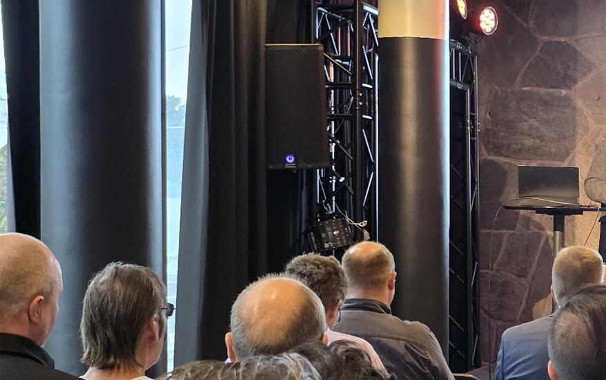

Artificial intelligence is rapidly moving from the cloud to the edge – into sensors, devices and machinery that operate close to where data is generated. This shift opens up tremendous opportunities but also introduces unprecedented risks.
- The cloud is just someone else’s computer, but the edge is in someone else’s hands, summarized Jaakko AlaPaavola, CTO of Etteplan, in his keynote at Embedded Conference Finland 2025 (main photo). His message was clear: trust and security are the foundation on which edge intelligence must be built.
Edge AI brings benefits that the cloud cannot always match: ultra-low latency, the ability to function without connectivity, and the option to keep sensitive data locally on the device. In many industrial or regulated environments, sending raw data to the cloud is impractical or even forbidden. Yet, as Ala-Paavola reminded, the lack of physical control raises the attack surface. Edge devices can sit in a mine, a vehicle, or a consumer’s home – where default passwords, open interfaces and outdated hardware become real vulnerabilities.
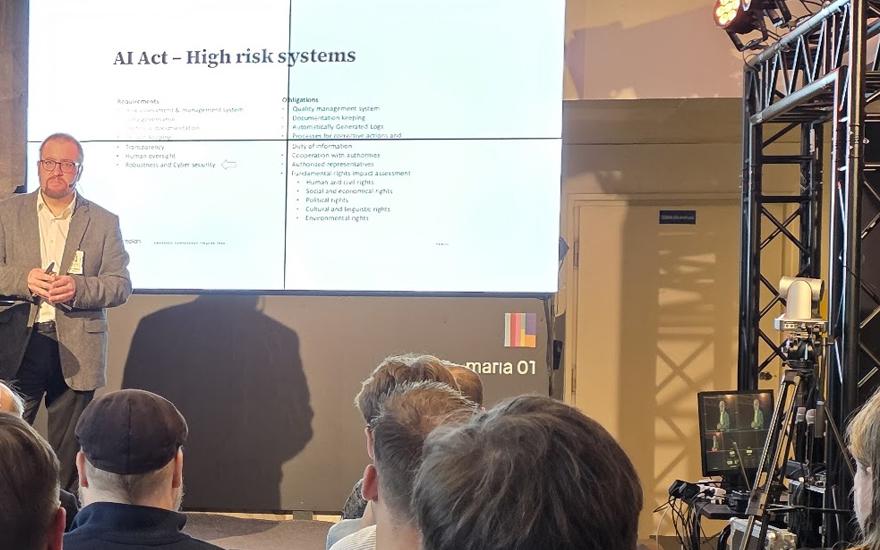
The European regulatory landscape is also pushing the industry forward. Laws such as the AI Act, the Cyber Resilience Act (CRA), NIS2 and GDPR all demand manufacturers to secure their devices and applications. By 2027, high-risk AI systems will be subject to requirements as strict as those governing medical devices. Some applications – such as real-time biometric recognition or emotion tracking – are banned altogether. Ala-Paavola emphasized that protection must be multilayered: from TPM modules and secure boot at the platform level, to
model protection against adversarial attacks, to strict data governance.
- Edge AI offers huge opportunities – but only if its security is strong. Without that, risks can outweigh the benefits, he concluded.
Security at the edge is not only a technical matter but also a regulatory one. Joe Hill of Digi International highlighted how the Cyber Resilience Act fundamentally transforms product development in Europe. CRA integrates cybersecurity into the CE marking, making security compliance mandatory for every digital product placed on the EU market. Manufacturers and distributors alike must ensure continuous protection throughout the product’s lifecycle – not only at launch.
Key obligations include rapid vulnerability reporting (within 24 hours), risk classifications, audits, encrypted data storage, secure OTA updates and a ban on weak defaults like hardcoded passwords.
Failure can result in sales bans, product recalls, or fines up to 2.5% of global revenue. Hill described CRA as a paradigm shift in product liability, and Digi showcased its TrustFence and ConnectCore Security Services as frameworks for ensuring compliance and long-term trust in connected devices
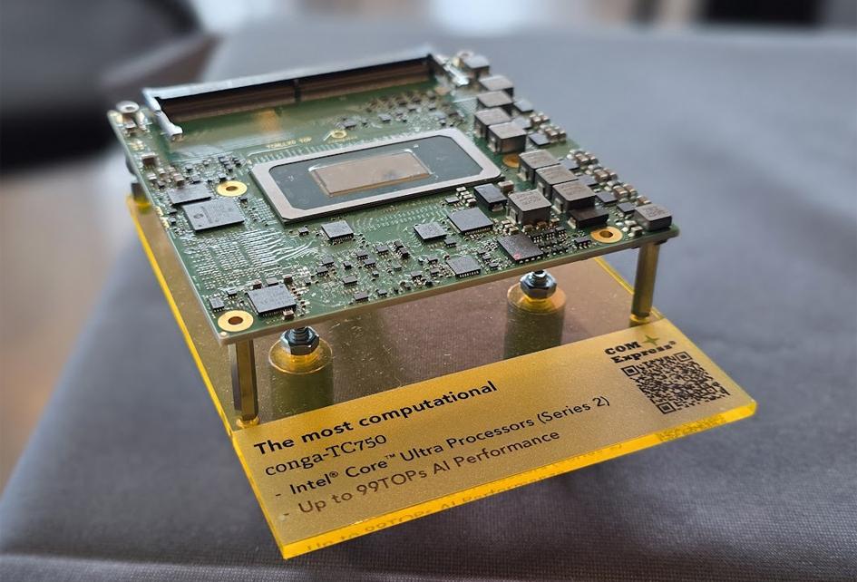
The conga-TC750 is a powerful COMExpress module. It brings up to 99 TOPS performance to AI inferencing at the edge (below, left).
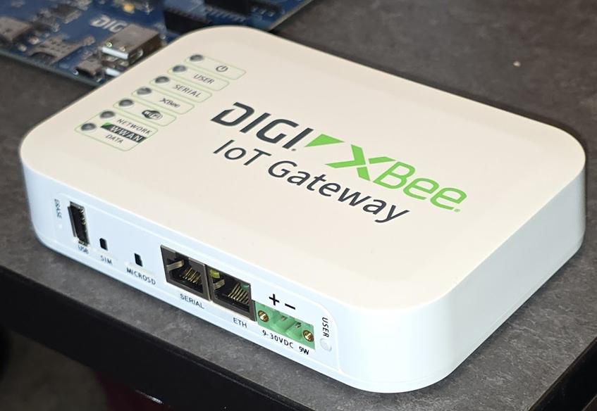
Digi Xbee IoT gateways are programmable converts wireless protocols like Zigbee, DigiMesh, or LoRaWAN to cellular. The gateway acts as a bridge between an enterprise LAN and the Internet (right).
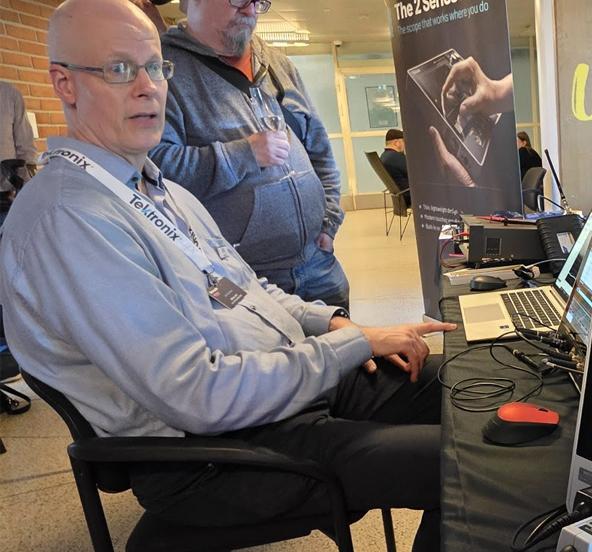
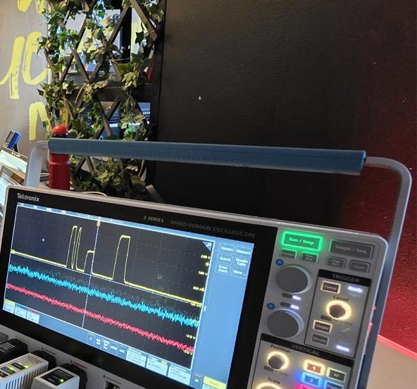
Mika Joutsila of BBC Solution (below) showed testing solutions for optical networks. The company specialices in DWDM and CWDM networks, optical transceivers, fiber network splicing and measurement techniques, networking products, fiber optic network solutions, and modern measurement and testing solutions, such as simulators, analyzers, as well as maintenance and calibration accessories.
From the hardware side, congatec’s Timo Poikonen underlined that in industrial environments, reliability is not a valueadd but an absolute requirement. Congatec has shipped more than 10 million modules worldwide and is known for its role in open standards like COM Express and SMARC. Now, the company is extending reliability from hardware into software and lifecycle management.
In partnership with Canonical, Congatec is certifying its modules for Ubuntu Pro LTS, ensuring up to ten years of validated updates. This is crucial for industrial systems with lifespans well beyond a decade. Without systematic updates, security holes and compatibility issues accumulate. Congatec’s aReady solutions offer preconfigured environments for virtualization and IoT management, enabling remote BIOS updates, mass configurations and secure cloud integration.
Virtualization plays a central role: Congatec’s upcoming IEC 62443-certified hypervisor allows multiple operating systems to run securely on a single module, directly addressing industrial cybersecurity requirements. A Japanese customer has already consolidated seven separate computers into one hypervisorcontrolled module, saving costs and simplifying updates while maintaining long-term security
Finally, Tiitus Aho of Tria Technologies argued that design strategies themselves must adapt to the new era of trust and regulation. The traditional chip-down approach may offer theoretical cost benefits but comes with higher risks, longer development cycles and resource bottlenecks. By contrast, Computer-onModule (CoM) solutions provide validated, updatable building blocks that reduce time-to-market, ease regulatory compliance and strengthen overall resilience.
In one customer case, CoM-based design cut time-to-market by more than a year while ensuring smooth deployment across multiple applications.
Standardized modules also reduce vendor lock-in, since multiple suppliers can support the same form factors. Aho framed modularity as more than a technical decision: it is a strategic choice that affects business speed, risk, and future competitiveness
Across the sessions at ECF25, a clear message emerged: the future of embedded systems and edge intelligence hinges on trust. This trust is not a single feature but an ecosystem built from regulation, lifecycle management, layered security, and strategic design choices

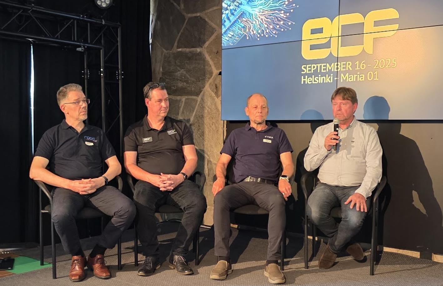
The electronics distribution industry is undergoing a profound transformation, driven by artificial intelligence, digitalization, and the new generation of engineers. At the ECF25 conference, industry leaders described the future of distribution as a balance between two forces: fully digital self-service and locally delivered, value-adding expertise.
The traditional three-tier model of distribution — broadline, specialized, and catalog-based — has effectively collapsed. To succeed, distributors must now operate as hybrids, combining online convenience with in-depth technical and customer knowledge.
Generation Z engineers, who manage the entire design and procurement journey digitally — from component selection to lifecycle management — are redefining expectations. This shift forces distributors to rethink their role and how they engage with customers.
- A webshop and a credit card are no longer enough to stand out,” said Jan Hellgren, CEO of Acal BFi. - A local distributor is taking that one extra step
on behalf of the customer, added Tiitus Aho of Tria Technologies.
At the same time, major global players like Amazon and Alibaba are pushing into the distribution market, intensifying price competition. In response, regional distributors are differentiating through expert services such as prototyping, proof-of-concept projects, precertifications, and ongoing design support.
All panelists agreed that AI will reshape distribution across the board — from design and logistics to customer support. It helps predict demand, optimize inventory, and accelerate technical assistance.
- AI must be part of the entire lifecycle, from design to end-of-life. When the customer asks ‘what’s the price and when can I get it,’ it’s already too late — we need to be one step ahead, emphasized Jan Hellgren.
AI is also empowering customers directly. Aku Wilenius from CN Rood highlighted National Instruments’ Nigel, an “engineer’s
ChatGPT,” which helps analyze measurement data and optimize design. Tiitus Aho sees AI as a tool to smooth out business cycles, forecast demand spikes, and reduce inventory risks — persistent challenges in distribution.
Still, everyone agreed that AI cannot replace local insight.- Specialized distributors know their customers better — their needs and preferences. Through local distributors, technical support and logistics become easier to deliver,” noted Joe Hill from Digi International.
Market cycles have diverged sharply. Consumer electronics remain sluggish, while defense, energy, and electrification sectors are driving demand. The panel agreed that real, broad-based growth will likely emerge around mid-2026.
- We see strong momentum in defense and energy, but weak demand near the consumer,” said Hellgren.
- Inventory built up during the pandemic has finally been cleared,” added Hill. “Order books are turning positive again, though recovery remains uneven.
As industries digitalize and products become smarter, embedded systems are at the heart of this transformation. Jenni Tuulos, Head of Embedded Development at Etteplan Finland, describes a market in transition — where AI, security, and energy efficiency are shaping the future of design.
- In Finland, embedded systems development is strongly tied to industrial digitalization, security, and the energy transition. We see the fastest growth in industrial IoT, energy and defense sectors, and intelligent human–machine interfaces. Today, integrating AI into products and services is a topic in nearly every customer discussion.
However, not every area has developed as expected.- There are also areas where growth hasn’t quite taken off as anticipated. For example, lifecycle management and maintenance often remain in the background, even though they account for a significant share of a product’s total cost. There’s great potential to create customer value here, for instance, by bringing secure-by-design thinking more firmly into the risk management of connected embedded systems already in the design phase.
GENERATIVE AI IS RESHAPING THE DESIGN CULTURE
Etteplan has been leveraging generative AI for years, particularly in technical documentation. Its influence on embedded systems design is growing more gradually. Tools like GitHub Copilot improve productivity, while AI helps engineers quickly access standards and design guidelines.
This shift goes beyond tools — it’s cultural.- We’ve introduced Etteplan rAIse service to support engineers in using GenAI responsibly. We’ve also renewed processes and invested heavily in competence development. For us, this isn’t optional: adopting new toolsand methods is essential to stay competitive.
LOW-CODE AND NO-CODE REMAIN EXPERIMENTAL
Although embedded design remains close to hardware, Tuulos sees new approaches starting to emerge.
- Embedded design is still deeply tied to hardware. C programming and low-level optimization are essential for resource efficiency and real-time performance. However, low-code and no-code (LCNC)
tools are starting to appear, mainly for rapid proof-of-concept prototyping.
- LCNC offers speed and accessibility, but struggles with scalability and complex logic. For now, these tools are mostly experimental because embedded systems demand precise resource control, which LCNC platforms can’t yet deliver for performance-critical usecases.
This year’s big themes include AI, IoT and embedded security, low-power systems, edge computing, and RISC-V.
deployed in industrial environments.
- IoT and energy efficiency are present in nearly every project we do. RISC-V, while promising, hasn’t yet translated into strong customer demand. The ecosystem is maturing, but for now, ARM remains the dominant choice for general-purpose embedded systems.
“A huge opportunity to do things smarter
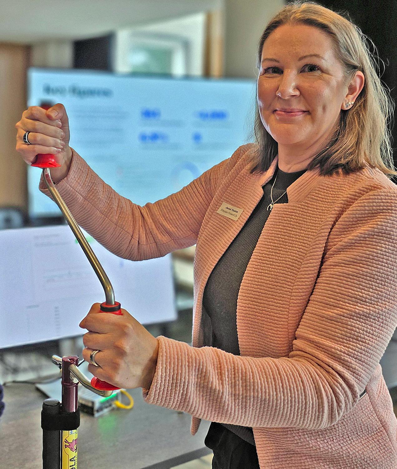
- AI isn’t replacing engineering expertise — it’s amplifying it. The real transformation happens when we combine human creativity, data-driven design, and secure technology to create smarter, more sustainable solutions. That’s what motivates our teams every day, says Jenni Tuulos, Head of Embedded Development, Etteplan.
- In our projects, AI and edge computing stand out — especially when combined with security. Secure Edge AI is gaining real momentum, and we expect demand for Edge AI solutions to grow significantly in the coming years. We also see modular automation platforms, such as ctrlX, influencing how edge intelligence is
— and more responsibly”. When asked what excites her most, Tuulos is clear: - I’m particularly excited about combining AI, security, and EU regulations — like the AI Act and Cyber Resilience Act — into practical solutions. There’s a real opportunity to make things both smarter and safer.
CN Rood’s new Country Manager in Finland, Aku Wilenius, believes that local expertise and support are essential for Finnish customers. He sees strong growth potential in testing and measurement solutions, especially in energy, 6G, and industrial digitalization.

The Finnish market may be limited in size, but it is significant and technologically demanding relative to its scale. According to Aku Wilenius, Finnish companies are usually highly skilled, which means they expect their suppliers to understand applications, not just products. Local expertise, service availability, high reliability, and quick response times are all crucial factors.
Wilenius sees several areas in Finland where demand for testing and measurement solutions is growing. Battery and energy technologies are developing rapidly, wireless technologies and 6G are advancing with Finnish research and industry at the forefront, and industrial digitalization and automation increasingly require comprehensive testing to ensure quality and safety. Critical infrastructure and defense projects also play a role in this development.
CN Rood stands out from many competitors by not representing just a single brand. Instead, it builds solutions by combining technologies from multiple manufacturers, providing customers with more flexible options. According to Wilenius, customers no longer seek individual devices but expect integrated solutions where measurement data flows seamlessly through software to the cloud and into analysis tools. Testing is becoming a more central part of corporate strategy, and interest in applying
artificial intelligence is on the rise.
Looking ahead, Wilenius expects growth particularly in energy and battery technology, electronics, embedded systems, sensor testing, and telecommunications. He believes CN Rood can realistically multiply its business in Finland by deepening existing customer relationships and building new partnerships with research and industry.
The company’s differentiation strategy rests on three pillars: a broad portfolio of suppliers, deep technical expertise and customer understanding, and local presence. CN Rood’s team in Finland is still small, but the ambition is to grow and ensure that customers receive reliable and fast support. - An international manufacturer can deliver the technology, but without a local partner the customer may feel left without support. That is why we invest in local service. It builds trust and strengthens collaboration, Wilenius emphasizes.
On a broader level, CN Rood gives Finnish companies more direct access to the latest technologies and expertise in testing and measurement. Wilenius hopes this will accelerate innovation, shorten development cycles, and strengthen Finland’s research, development, and technology production ecosystem.
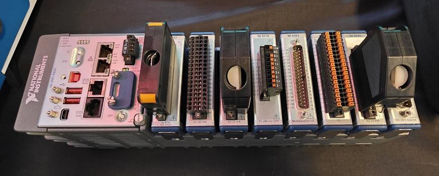
NI’s CompactRIO platform combines a real-time processor with an FPGA to deliver reliable performance, precise timing, and a flexible software toolchain for Industrial IoT, monitoring, and control
Aku Wilenius recently joined CN Rood as Country Manager for Finland. Previously, he led National Instruments’ operations in the country. At NI, he learned the importance of long-term customer relationships and technical expertise, as well as the value of combining hardware and software into seamless systems. Those lessons, he says, are now being applied at CN Rood.
Microchip Technology has introduced its next generation of Switchtec Gen 6 PCIe Switches. The industry’s first PCIe Gen 6 switches manufactured using a 3 nm process, the family is designed to deliver lower power consumption and support up to 160 lanes.
Advanced security features include a hardware root of trust and secure boot, utilizing post-quantum safe cryptography compliant with the Commercial National Security Algorithm Suite (CNSA) 2.0.
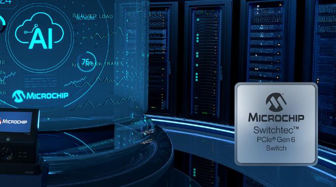
Previous PCIe generations created bandwidth bottlenecks as data transferred between CPUs, GPUs, memory and storage, leading to underutilization
and wasted compute cycles. PCIe 6.0 doubles the bandwidth of PCIe 5.0 to 64 GT/s (giga transfers per second) per lane, providing the necessary data pipeline to keep the most powerful AI accelerators consistently supplied.
Switchtec Gen 6 PCIe switches enable high-speed connectivity between CPUs, GPUs, SoCs, AI accelerators and storage devices, and are designed to help data center architects scale to the potential of next generation AI and cloud
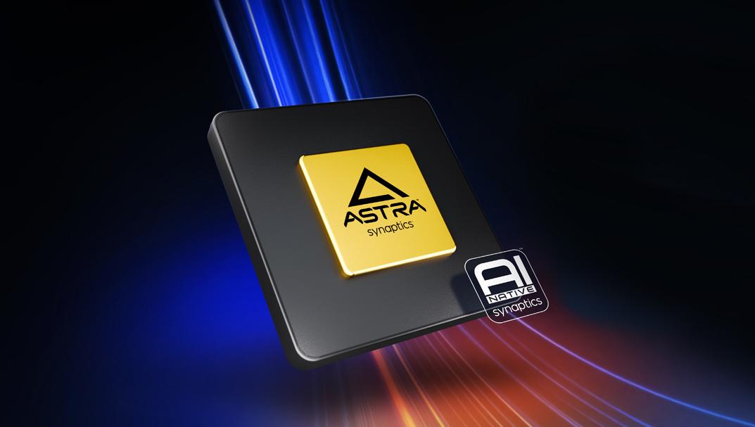
Google’s Coral AI accelerator is making the leap from research labs to commercial deployment in Synaptics’ new Astra SL2600 series of processors. This marks the world’s first production-grade processor family to leverage Google’s open, RISC-V–based Coral NPU, opening a new chapter in the Edge AI market long dominated by closed, Arm-based solutions.
Synaptics’ Torq subsystem represents the first commercial implementation of Google’s Coral processor. It is part of the Astra SL2610 product line, designed to move AI inference from the cloud directly to edge devices. The series includes five pin-compatible chips targeting applications such as industrial automation, smart home devices, robotics, and healthcare systems.
The Coral processor’s power consumption stays below ten milliwatts — a fraction of that of current NPU cores such as Arm’s Ethos-U85. This makes it an exceptionally attractive solution for low-power, batteryoperated AI devices. At the same time, the Torq architecture and its software framework — built on the open IREE/MLIR compiler technology — allow developers to run virtually any AI model without the
constraints of closed ecosystems.
The Edge AI market has long been fragmented. Each vendor has developed its own incompatible compilers and toolchains, slowing down the scalability of AI solutions. Synaptics’ strategy is built on open-source software and a partner ecosystem that includes not only Google but also companies like Arm, Cisco Systems, and Deutsche Telekom.
This development could change the dynamics of the entire market. IDC projects that the AI inference processor market will grow to 23.6 billion USD by 2029. If the open Coral architecture and Synaptics’ Torq development environment prove successful, other semiconductor manufacturers are likely to follow the same path.
Synaptics’ SL2610 series processors are now sampling and will reach general availability in the second quarter of 2026. By then, many competitors will likely be working on their own versions of the Coral core — but Synaptics will be remembered as the first company to bring Google’s open AI processor to commercial silicon.
Infineon Technologies has introduced a new generation 60gigahertz radar chip designed especially for low-power IoT applications. The company’s XENSIV BGT60CUTR13AIP is based on CMOS technology and offers a highly compact, energyefficient, and easily integrable solution for smart devices. The new chip is equipped with its own processor and hardware accelerator, enabling data processing directly on the chip and reducing the load on the main processor. This makes systems smaller, more costeffective, and more energyefficient.
MIPS, which now is a part of GlobalFOundries, has announced the new MIPS I8500 processor, designed specifically for eventdriven computing in the age of artificial intelligence. The new processor represents the third generation of a four-threads-percore architecture based on the open RISC-V instruction set. The architecture of the MIPS I8500 is designed to be deterministic and scalable. Each core features four threads, and up to six cores can be combined into clusters — for a total of up to 1,536 parallel threads. This enables highly efficient, low-latency processing of multithreaded data streams.
infrastructure. By acting as a highperformance interconnect, the switches allow for simpler, more direct interfaces between GPUs in a server rack, which is crucial for reducing signal loss and maintaining the low latency required by AI fabrics.
The PCIe 6.0 standard also introduces Flow Control Unit (FLIT) mode, a lightweight Forward Error Correction (FEC) system and dynamic resource allocation. These changes make data
transfer more efficient and reliable, especially for small packets which are common in AI workloads. These updates lead to higher overall throughput and lower effective latency.
The switches feature 20 ports and 10 stacks with each port featuring hot- and surprise-plug controllers. Switchtec also supports NTB (Non-Transparent Bridging) to connect and isolate multiple host domains and multicast for one-to-many data distribution within a single domain.
Researchers from the Max Planck Institute and the University of Oxford have successfully controlled a completely new class of materials—so-called ferroaxial materials—using ultrafast light pulses. The discovery could pave the way for an entirely new generation of data storage: faster, more stable, and more energy-efficient nonvolatile memories. In ferroaxial materials, electric dipoles do not point in a single direction as in ferroelectric materials, but instead form swirling structures that can twist either clockwise or counterclockwise. These two states can function like “bits” in digital memory.
The development of quantum computers took a major leap forward when Caltech researchers announced they had built a record-breaking quantum machine. The new device contains as many as 6,100 neutral-atom qubits, making it the largest qubit system ever assembled. Previously, similar machines reached only a few hundred qubits.
Quantum computers differ from classical computers in that their qubits can exist in two states simultaneously—an effect known as superposition. This allows them to carry out complex calculations far more efficiently than traditional bits, but it also makes qubits extremely fragile and prone to errors. For this reason, researchers aim to build machines with vast numbers of additional qubits dedicated to error correction.
The Caltech team used optical tweezers— highly focused laser pulses—to trap individual cesium atoms in a grid suspended in a vacuum. They managed to split a single laser beam into 12,000 “tweezers,” more than half of which were filled with atoms. This resulted in a system of 6,100 qubits.
But sheer number was not the only achievement. The team demonstrated that the qubits remained in superposition for nearly 13 seconds—ten times longer
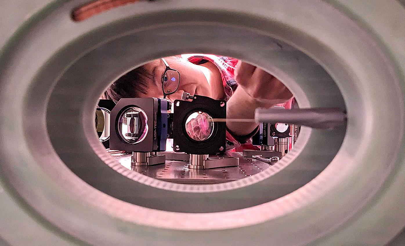
than in previous similar systems. In addition, the control of individual qubits was achieved with near-perfect accuracy of 99.98 percent. This is crucial, since qubits are useless without quality.
Another significant breakthrough was the ability to move atoms across the grid over long distances without disturbing their state. This feature could give neutral-atom machines an advantage over superconducting quantum computers, whose architecture is rigid and where qubits are fixed in place by wiring.
The European Association of Research and Technology Organisations (EARTO) has awarded Finnish company SemiQon and VTT Technical Research Centre of Finland first place in the Impact Expected category of its 2025 innovation competition. The recognition, announced in Brussels on October 14, celebrates groundbreaking work on cryogenic CMOS chip technology designed for quantum computing and space applications.
The awarded technology enables siliconbased CMOS chips to operate at extremely low, cryogenic temperatures, unlocking new possibilities for quantum computing and space electronics, where conventional chips struggle to function efficiently.
CMOS (Complementary Metal-Oxide Semiconductor) is the standard technology used in nearly all modern microchips. SemiQon’s innovation, cryogenic CMOS (Cryo-CMOS), allows

these chips to maintain full performance at temperatures close to –270°C. This is essential for future quantum processors, as the control electronics must function in the same ultra-cold environment as the quantum bits (qubits) themselves.
SemiQon CEO Himadri Majumdar notes that cryogenic electronics are moving rapidly from niche to mainstream.“While the field may still seem small today, it will soon become central—driven by quantum computing and space technologies. We are honored by this recognition, which highlights both the
The researchers compare moving an atom while keeping it in superposition to a delicate trick: it’s like trying to run steadily with a full glass of water without spilling a single drop. Now, this feat has been achieved on the scale of thousands of atoms.
The next major milestone is to establish entanglement within such a vast qubit system. Only through entanglement can quantum computers realize their full power and simulate natural phenomena, such as new phases of matter or the quantum fields that shape spacetime.
potential and the impact of our technology,” Majumdar says.
The new CMOS technology offers exceptional energy efficiency and performance. It eliminates the power consumption and heat dissipation problems that have previously limited CMOS adoption in cold environments. In space applications, it can cut power usage by 50–90%, while in quantum computing infrastructure it can reduce readout system costs by up to 30%. Over time, the savings could multiply, with global cooling-related cost reductions reaching $20–30 billion annually.
The technology was originally developed at VTT, from which SemiQon was spun off in 2023. The company manufactures its chips at Micronova in Espoo, Finland, and will later expand production to Kvanttinova, a new cleanroom facility designed for both industrial and research use.
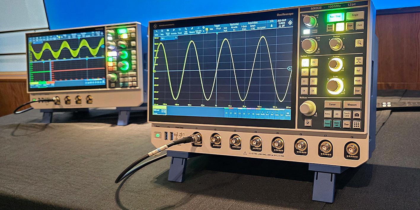
Rohde & Schwarz has introduced the new MXO 3 oscilloscope series, bringing high performance and eight-channel measurement capability to a compact form factor. Positioned between the company’s MXO 4 and RTM3000 lines, the MXO 3 takes sub-1 GHz oscilloscopes to an entirely new level of speed and precision.
Built on the same MXO-EP ASIC platform as the larger eight-channel MXO 5, the MXO 3 delivers up to 400 Gbps processing performance and an acquisition rate of 4.5 million waveforms per second. According to R&S, the proprietary ASIC enables the instrument to capture up to 99 percent of real-time signal activity, making it the fastest oscilloscope in its class below 1 GHz.
The series is available in four- and eightchannel models with bandwidths ranging from 100 MHz to 1 GHz. Standard memory depth is 125 Mpoints, expandable to 500 Mpoints, while 12-bit hardware resolution and an HD mode offering up to 18 bits ensure excellent signal-to-noise ratio and measurement accuracy. Compared with its predecessor, the RTM3000, the MXO 3 provides four additional channels, a
redesigned SmartGrid user interface, and significantly higher acquisition performance.
With its 11.6-inch Full HD display, modern UI, and compact 4 kg chassis, the MXO 3 fits comfortably in both bench and field environments. The instrument integrates multiple functions — oscilloscope, spectrum analyzer, logic and protocol analyzer, digital multimeter, and optional waveform generator and Bode (FRA) analysis — into a single, space-saving unit.
R&S positions the MXO 3 particularly for power-measurement and embeddedsystem applications, where multi-channel, high-precision analysis is essential. The targeted market segment covers frequencies below 1 GHz, where all major vendors compete on a balance of performance and affordability.
Pricing starts at €5,350 for the fourchannel 100 MHz base model and reaches approximately €36,000 for the eightchannel 1 GHz version. Bandwidth upgrades can be enabled at any time via software license.
JEDEC says it is nearing completion of the next version of its highly anticipated Universal Flash Storage (UFS) standard: UFS 5.0. Designed for mobile applications and computing systems that demand high performance with low power consumption, UFS 5.0 plans to deliver faster data access and improved performance compared to its predecessor, while maintaining compatibility with UFS 4.x hardware.
UFS leverages industry-leading specifications from the MIPI Alliance to
form its Interconnect Layer. This collaboration continues with UFS 5.0, which leverages the upcoming MIPI MPHY® version 6.0 specification and the UniPro version 3.0 specification. M-PHY 6.0 introduces a new High-Speed Gear 6 (HS-G6), which supports data rates double those of the previous maximum data rate of HS-G5, enabling UFS interface bandwidth of 46.6 Gb/s per lane and supporting up to ~10.8 GB/s effective read/write operation for UFS 5.0 over 2 M-PHY lanes.
QMill of Finland has developed a record-breaking method for compressing quantum circuits, bringing useful quantum computations closer in time. QMill demonstrates its capability by sharing QASM files of several benchmark circuits and their compressions. One of these circuits was compressed to just half the size of the previous best result. Results are assuring. For example the circuit referred to as MOD5_4, which originally had 71 gates, was reduced to 24 gates by our method — less than half the size achieved by Quarl, which compressed it to 50 gates.
Analog Devices has introduced the new ADI Power Studio platform, which unifies the company’s power design tools into a single ecosystem and delivers a major upgrade to webbased power design. The platform aims to streamline the entire design process—from system level down to circuit level. Among the new features are Power Studio Planner and Power Studio Designer, modern browser-based tools that support designers from power distribution network planning to component selection and performance simulation.
Vodafone has carried out the world’s first mobile network test in the 6 GHz frequency band using a standard smartphone and a commercial MediaTek M90 modem. The test demonstrates that the 6 GHz band offers excellent potential for both advanced 5G and future 6G technologies. The experiment took place in Hanover, Germany, using a 200 MHz bandwidth, and the results were impressive: download speeds reached 2.5 gigabits per second—faster than current average 5G connections. Moreover, the 200 MHz channel provided double the data transfer capacity compared to a 100 MHz channel, without any increase in energy consumption.
Securing wireless networks is one of today’s most difficult cybersecurity challenges. Traditional solutions such as WiFi and other radio frequency–based systems easily leak into their surroundings. They can be detected, jammed, and even intercepted from a distance. To address this vulnerability, a new technology has emerged: LiFi, which transmits data using visible and infrared light.
Light-based connectivity differs fundamentally from radio. A LiFi signal does not penetrate walls but remains physically confined to a room or defined space. This makes unauthorized listening far more difficult. Since the system does not use radio frequencies, its electromagnetic footprint is nearly zero. The signal cannot be detected or jammed by conventional means.
Furthermore, pureLiFi has built its systems on the familiar IEEE 802.11 family of protocols. That means LiFi can be deployed much like WiFi but with significantly stronger protections layered on top. These include WPA3 Enterprise encryption with 256-bit keys, device tracking, and geofencing capabilities.
The benefits of LiFi are most visible in defense and security contexts. The U.S. Army has tested the technology in Europe and Africa with promising results. In tactical field operations, command posts can be set up more quickly because the need for extensive cabling is reduced. At the same time, troops’ risk of detection is minimized, as the near-zero electromagnetic signature does not reveal their position.
LiFi has also proven useful for updating vehicles and aircraft with data securely and rapidly, without the risk of interference. It enables wireless connectivity in environments where radio frequencies are forbidden or hazardous, such as ammunition depots, hospitals, or chemical facilities. Autonomous systems like drones also benefit from LiFi, which allows them to build encrypted, hard-todetect mesh networks and transfer mission-critical data discreetly.

An international research team has achieved a new record for the efficiency of perovskite–silicon hybrid, or tandem, solar cells. Through passivation, the cells reached an efficiency of 33.1 percent and an open-circuit voltage of 2.01 volts — a clear improvement over previous results.
The research was carried out by the King Abdullah University of Science and Technology (KAUST), the University of Freiburg, and the Fraunhofer Institute for Solar Energy Systems (ISE). The breakthrough came from successfully applying passivation to textured silicon cells, which are commonly used in today’s photovoltaic industry. Previously, effective passivation had only been achieved on flat surfaces.
Passivation improved not only the voltage but also the cell’s conductivity and fill factor. Unlike in silicon cells, where the treatment affects only the surface, in perovskites the passivation

extends throughout the entire layer, enhancing the material’s bulk properties as well.
According to the researchers, this is a significant step toward the industrial production of tandem solar cells. The theoretical efficiency limit of silicon cells
(29.4%) has been nearly reached, and the perovskite–silicon combination offers a pathway to surpass it.
The study was published in Science and is based in part on projects funded by the German Federal Ministry for Economic Affairs and Energy.
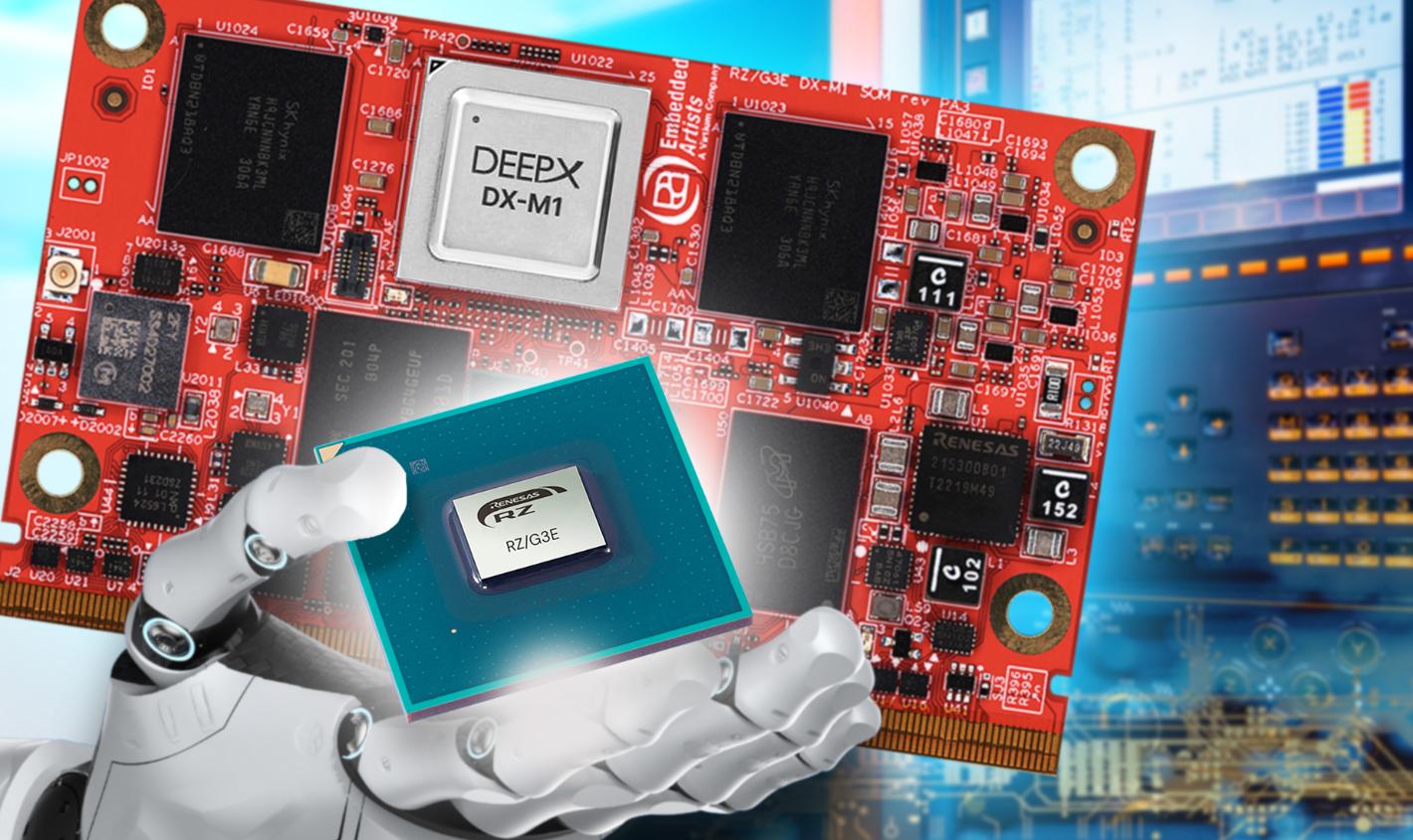
Local AI computing is making a strong entrance into embedded systems. The Sweden-based company Virtium Embedded Artists has introduced a new RZ/G3E System-on-Module (SOM) solution that brings artificial intelligence and advanced user interfaces directly to the network edge — without the need for a constant cloud connection.
The new module is built on Renesas’ RZ/ G3E processor and features four Arm Cortex-A55 cores, one Cortex-M33, and integrated graphics and video accelerators. The hardware supports dual Full HD displays, H.264/H.265 codecs, and 3D graphics, making it an ideal platform for demanding industrial and medical HMI applications.
But the real breakthrough lies in AI capability. The module offers two alternative AI implementations: an
Nordic Semiconductor, has announced the availability of nuSIM for its nRF91 Series of cellular IoT modules. This innovative, software SIM solution eliminates the need for a physical SIM card and socket, allowing product developers to reduce device size, simplify manufacturing, and enhance the robustness of their cellular IoT designs.
NuSIM is an open standard approach to integrated SIM (iSIM) where SIM credentials are encrypted and managed within a secure, protected area of the device. By operating as a dedicated software component inside the secure Arm TrustZone® of the nRF91 Series’
integrated Arm Ethos-U55 NPU for lightweight audio, image, and sensorbased applications, delivering 0.5 TOPS of performance; and a version equipped with DeepX’s DX-M1 accelerator, boosting performance up to 25 TOPS — enough for complex, real-time inference without cloud computing.
“This SOM is the fastest way to integrate the RZ/G3E processor into systems that require high-end HMI capabilities. At the same time, it brings AI directly to the edge — right where the data is generated,” says Anders Rosvall, CEO of Virtium Embedded Artists.
Development is supported by a comprehensive set of Linux software packages and an extensive development board that speeds up both prototyping and final product design..
The Dutch government has made an exceptional decision to assume control of the Chineseowned semiconductor manufacturer Nexperia. The decision was based on the Goods Availability Act, a law that has been used extremely rarely in the country’s history. The move aims to safeguard the continuity of Europe’s semiconductor supply and prevent critical technological expertise from falling under Chinese influence. The Ministry of Economic Affairs justified the action by citing “serious administrative deficiencies” and “acute signals” in the company’s operations that threatened the economic security of the Netherlands and Europe.
Melexis has launched the MLX90514 chip, the world’s first inductive position sensor capable of reading two coil setups simultaneously on a single chip. This new solution enables differential and Vernier angle calculations directly on the chip without the need for external processing. The dualchannel architecture addresses the growing demands of electric and autonomous vehicles, where precision, synchronization, and safety are critical. In particular, for steer-by-wire, torque, and angle sensing applications, the MLX90514 provides fully synchronized, zero-latency measurement from both channels
application processor, nuSIM removes all external SIM hardware, directly reducing the bill of materials (BOM) and saving valuable board space. This is ideal for cellular IoT devices deployed in harsh environments—for example in water metering or smart farming irrigation applications—as removing the SIM socket eliminates a common point of mechanical failure and protects against corrosion and vibration.
The fully digital provisioning process streamlines the supply chain, allowing SIM profiles to be securely delivered to devices during manufacturing, simplifying logistics and reducing operational costs.
Arduino has introduced the new Arduino UNO Q board — the first device in the UNO series capable of running the Linux operating system. The new UNO Q is powered by Qualcomm’s Dragonwing QRB2210 processor, which brings a quad-core CPU, graphics and AI acceleration, and support for camera, audio, and display interfaces. The board features a so-called dual-brain architecture: alongside the Linux-running processor operates an STM32U585 MCU.
Ambient Scientific, a company specializing in AI processors, has introduced the new GPX10 Pro system-on-chip, designed from the ground up for artificial intelligence needs. According to the company, the chip delivers up to 100-fold improvements in performance and energy efficiency compared to traditional 32-bit microcontrollers.
The GPX10 Pro features ten programmable AI cores and is based on Ambient Scientific’s proprietary DigAn architecture, where neural network matrix multiplication and activation computations are performed directly in memory. This reduces the overhead of a traditional processor and enables AI models to run with very low power consumption. Described as a native AI processor, the chip can even operate on a coin cell battery.
The chip is particularly well-suited for battery-powered edge devices, such as voice recognition, facial recognition, and intelligent sensor fusion. The GPX10 Pro supports common neural network models (CNN, RNN, LSTM, GRU) and is capa-
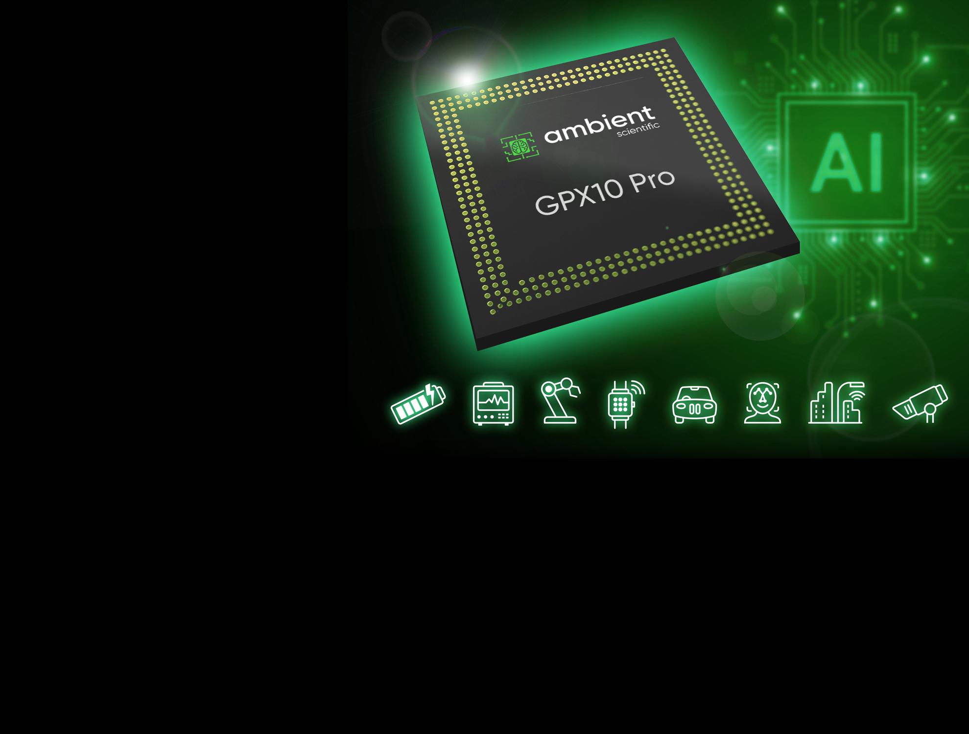
ble of AI performance up to 512 GOPs.
In addition, the chip includes an Arm Cortex-M4F control unit as well as a wide range of interfaces for analog and digital sensors. Ambient Scientific also provides the Nebula development tools for training and deploying models, as well as the SenseMesh sensor network, which enables ultra-fast and energy-efficient sensor data integration.
The first sample batches of the GPX10 Pro chip are already available, and volume production is expected to begin in the first quarter of 2026.
Advantech, a global provider of industrial edge computing and AI solutions, will return to the Teknologia 2025 exhibition in November with the goal of strengthening its foothold in the Finnish market. Key Account Manager Jonas Appelgren sees the event as a prime opportunity to build new customer relationships and partnerships.
- Teknologia is by far the most important event for us in Finland, as there are very few similar industry gatherings in this market. Since we don’t have a local office in Finland, the exhibition provides a valuable opportunity to meet potential customers and gain first-hand insights into the needs and trends of Finnish industry, Appelgren says.
According to Advantech, Finland is an attractive market, home to many pioneering companies that are quick to adopt new technologies.- Finland is known for its innovation and early adoption of new technologies. We see growing opportunities not only in industrial automation but also in

mission-critical and medical technology sectors, Appelgren notes.
The company is also looking to strengthen collaboration with local partners.- There’s limited direct design activity in Finland, but system integration and customization are strong areas. We want to engage more closely with the Finnish integrator and developer community, Appelgren adds.
At the Teknologia 2025 exhibition in Helsinki (booth 6g80), Advantech will showcase its latest edge computing and
AI solutions that help customers develop smarter, safer, and more scalable industrial applications.
One of the new products on display will be the ARK-1222, a compact DIN-rail mounted industrial computer designed for demanding environments and fanless operation. The device combines a rugged build with intelligent software integration, offering enhanced cybersecurity for next-generation edge applications.
Another highlight will be the AOM-5721, a SMARC module based on the Qualcomm QCS6490 chipset. Delivering up to 12 TOPS of AI performance at only 12 watts TDP, it is designed for compact, low-power Edge AI applications.
The booth will also feature a real-time object detection demo based on Advantech’s AOM-2721 development kit. Running Ubuntu 24.04, the system executes a PyTorch-based YOLOv8 model at up to 30 FPS, showcasing the efficiency of AI inferencing at the edge.
Intel has introduced its new Core Ultra Series 3 generation, codenamed Panther Lake — the company’s first consumer processor built using the entirely new 18A process technology. The launch marks a major turning point for Intel — both technically and strategically — as it aims to reclaim its position alongside competitors such as AMD, Apple, and Qualcomm.
The Panther Lake generation is built on Intel’s own 18A process, which combines the new RibbonFET transistor technology with PowerVia backside power delivery. The processors are manufactured at Intel’s new Fab 52 facility in Arizona, which the company describes as the most advanced semiconductor plant operating in the United States. Fab 52 is part of Intel’s more than $100 billion investment to strengthen domestic chip production.
Panther Lake introduces a multi-chip — or chiplet-based — architecture that scales performance and power efficiency across device classes, from thin laptops to highperformance gaming systems and edge computing devices.
The new Core Ultra Series 3 processors offer up to 16 P- and E-cores and deliver
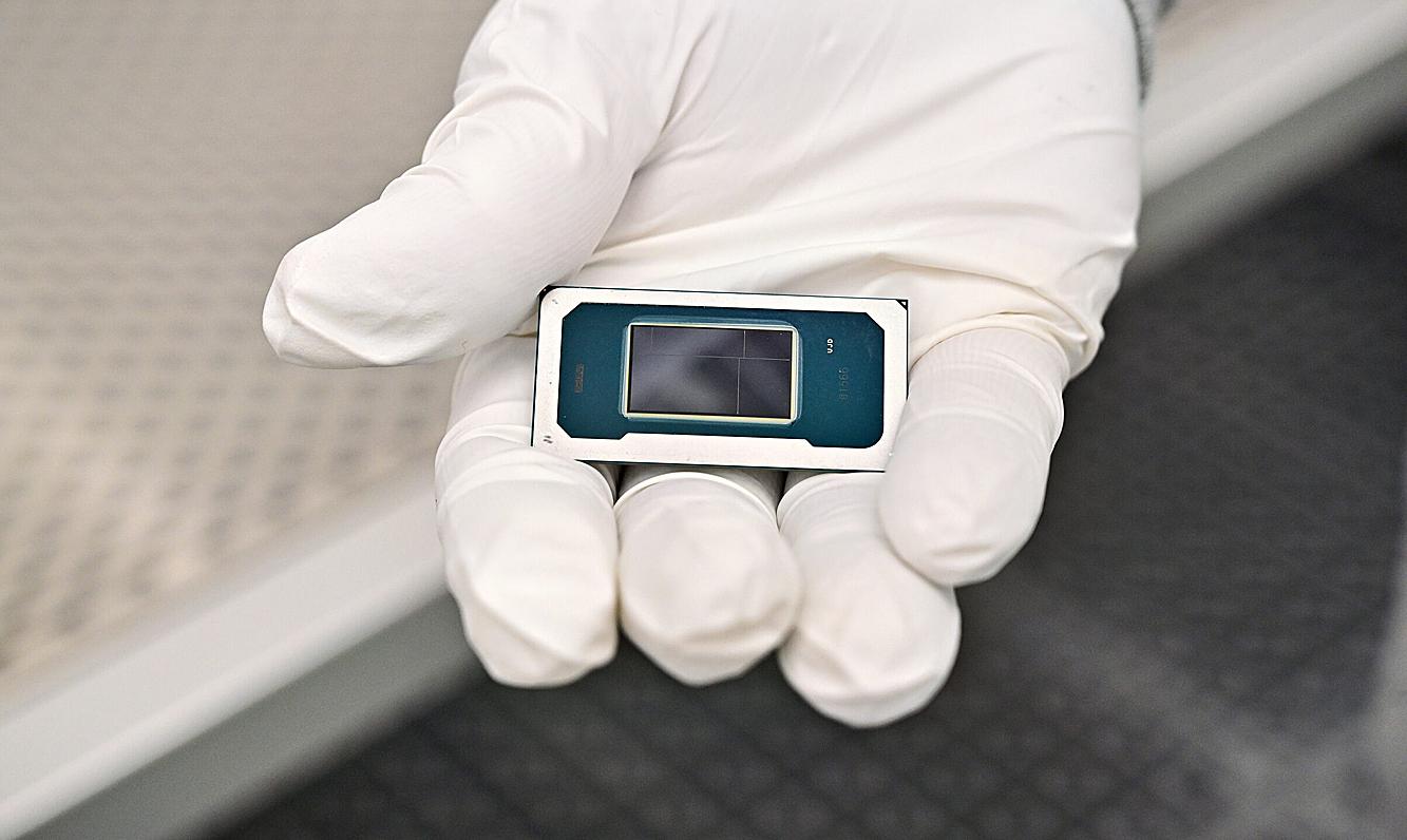
more than 50% faster CPU performance compared to their predecessors. The new Intel Arc GPU features up to 12 Xe cores and up to 50% improved graphics performance.
In AI computing, Panther Lake achieves up to 180 TOPS, representing a threefold increase in AI performance. In addition to this, the new processors deliver better en-
ergy efficiency than previous generations.
The first laptops powered by Panther Lake processors will reach the market in January 2026, with initial models expected to be completed by the end of 2025. Panther Lake also marks Intel’s first commercial product to fully utilize a leading-edge process developed and manufactured entirely in the US.
The world’s first and largest Sand Battery has been inaugurated in Pornainen, Finland. Developed by Polar Night Energy and commissioned by Loviisan Lämpö, the facility has been operating since June as the main production plant for the local district heating network, reducing emissions by around 70%.
The Sand Battery stores renewable electricity as heat in sand, providing affordable and reliable energy for homes and public buildings. In its first months of operation, it has exceeded performance targets and completely replaced the municipality’s old woodchip plant.
Backed by CapMan Infra, the investment demonstrates significant commercial potential. With large-scale storage capacity and advanced AI optimization by Elisa Industriq, the Sand Battery supports grid balancing, reserve market participation, and reduced dependence on single energy sources.

Polar Night Energy is preparing new projects in Finland and abroad, including industrial applications where high-
temperature heat is required, further expanding the role of Sand Batteries in the clean energy transition.
The microduct fiber network is reshaping urban data infrastructure. It cuts excavation, speeds expansion, and enables next-generation smart systems. Kuopio’s solution has become a model gaining international attention.


The microduct network not only streamlines but also rationalizes the ever-expanding foundation of smart cities and the refining of data for diverse applications. The solution enables the construction of communication infrastructure without the continuous excavation and traffic disruptions caused by traditional cabling.
–“The City of Kuopio has been building a microduct network alongside street renovations in the Savilahti district for six years now,” says Jari Torvinen, Chief Information Officer of the City of Kuopio.
According to Torvinen, the microducts have significantly improved the efficiency of network development. Sitowise Oy is also utilizing the same technology in major cities such as Tampere and Espoo.
Artificial intelligence now extends to automated traffic control and event monitoring, making real-time data transfer an essential part of urban functionality.
The development of data communication centers has brought intelligent data refinement into the daily operations of cities.
In Kuopio, traffic light control is optimized in real time, and waiting times at intersections in Savilahti have been reduced by 15 percent, cutting emissions and improving traffic flow.
Real-time parking space monitoring has also been adopted as part of the city’s smart infrastructure applications.
The core of microduct infrastructure lies in its unique installation method: compressed air propels the fiber cable through the duct, with a brass bullet attached to its end guiding it forward.
Hundreds of meters of microfiber rest in the ducts, ready for activation — with no need for new digging.
Although the technology is more expensive per unit than traditional fiber, its adoption has been slowed by incomplete cost-benefit assessments. When reduced earthworks and long-term savings are taken into account, the solution often proves to be economically sound.
At the same time, it helps avoid overlapping excavations by competing telecom operators working without an overall plan.
Growing data volumes cannot rely solely on mobile networks.
–“The amount of data is so large that mobile connections alone are not sufficient. Microfiber is needed for data transfer,” says Ville Pitkänen, CEO of Fibecon Oy.
To ensure reliable data transmission, parallel technologies are used. The microfiber method is particularly well suited for dense road surface sensor networks, where data between robotic vehicles and sensors updates within milliseconds — for example, during winter road cleaning and snowplowing operations.
Sitowise Oy regards Kuopio’s solution as an international benchmark for smart infrastructure development.
–“The scope of the plan is unique in Finland, perhaps even in all of Europe. The needs of smart infrastructure have been comprehensively integrated into the city’s planning and management,” says Samuli Virtanen, Project Manager at Sitowise.
The construction of Kuopio’s smart infrastructure extends through all aspects of the city’s planning, construction, and service development — with a vision stretching to 2050.


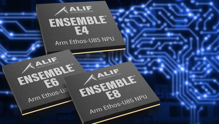
Alif Semiconductor founder Reza Kazerounian tells ETN that the true breakthrough for generative AI will come when it moves from the cloud to ultralow-power devices. Alif aims to bring AI to microcontrollers, enabling billions of edge devices to make real-time decisions without constant connectivity.
1. What inspired the development of the AI microcontroller, and what was the original direction?
From the beginning, Alif wanted to understand where the market was heading. Generative AI grew rapidly in the cloud and on large computers, but its true potential lies at the edge—in small, battery-powered devices. The idea was to break the barriers that prevented the use of advanced AI in wearables, industrial sensors, and medical solutions.
2. What is the role of the Arm Ethos-U NPU in the microcontroller?
The NPU works like a graphics processor for a small CPU: it offloads heavy neural network computation from the core and executes it with a parallel architecture. This brings up to more than a 100x performance improvement and allows the device to return to sleep mode faster, saving battery power.
3. What factors are most important in optimizing ultra-low power consumption?
The key is balancing performance and power consumption. Keeping data in fast
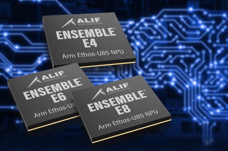
SRAM maximizes performance but increases power draw. Alif uses MRAM memory to store the fixed data of models, achieving a good compromise: dynamic data in RAM, permanent data in nonvolatile memory.
4. How important are development tools such as Conductor?
All productivity-enhancing tools are valuable. We don’t want to force developers into new closed platforms but instead enable the familiar Arm ecosystem tools. Conductor simplifies low-level configuration of Alif’s own chips—without any installations.
5. What kind of learning curve do developers face when AI is brought to MCUs?
Working with neural networks introduces new steps such as model selection, optimization, and building training datasets in the context of the application. In voice- and image-based applications, for example, language, dialects, or camera placement critically affect model quality.
6. Which applications benefit the most from on-device AI, and what still limits them?

Wearables and industrial applications are immediately beneficial, where low latency and fast response are essential. Wearables benefit from rapid computation on small batteries, and in industry, decisions can be made at the edge without heavy data transfer. New examples include even children’s toys, where generative AI creates dynamic experiences.
7. How far can AI realistically go in embedded systems?
Embedded devices will always have limitations compared to the cloud. The future solution is a hybrid model, where some functions are performed locally and others in the cloud. For example, smart glasses might locally handle only the country’s primary language but send other languages to the cloud for translation. Technology is advancing rapidly. We have only scratched the surface.


Yann LeFaou Microchip Technology
ML/AI takes edge processing to the next level by making at-source inference possible. It enables an IoT device, to stick with that example, to learn and improve from experience. Algorithms analyze data to look for patterns and make informed decisions with three ways in which the machine (or AI) will learn: supervised learning, unsupervised learning and reinforced learnings.
Supervised learning sees the machine using labeled data for training. For example, a smart security camera might be trained using photos and video clips of people standing, walking, running or carrying boxes. Supervised ML algorithms include Logistic Regression and Naive Bayes, with feedback required to keep refining the model(s) on which predictions will be made.
Unsupervised learning uses unlabeled data and algorithms such as K Means Clustering and Principal Component Analysis to identify patterns. This is ideal
Machine learning have traditionally platforms but data sources. devices, reduces improving performance enhancing security.

for anomaly detection. For instance, in a predictive maintenance scenario or medical imaging application the machine would flag situations or aspects of the image that are unusual based on the model of ‘usual’ that the machine has built and is maintaining.
Reinforced learning is a ‘trial and error’ process. As with supervised learning, feedback is required but, rather than simply correcting the machine, the feedback is treated as either a reward or a penalty. Algorithms include Monte Carlo and Q-learning.
In the above examples, a common element is embedded vision; made ‘smart’ through the addition of ML/AI and any other applications can benefit from vision-based, at-source inference. Moreover, smart embedded vision can use parts of the spectrum not visible to the human eye, such as infrared (used for thermal imaging) and UV.
Provide an ML/AI edge system with other data, such as temperature readings and vibration levels from transducers, and industrial IoT devices can not only play a significant role in an organization’s predictive
learning (ML) and artificial intelligence (AI) traditionally run on high-performance or cloud but are now increasingly deployed near sources. This edge processing, ideal for IoT reduces the need to send data to the cloud, performance through lower latency and security.

maintenance strategy, but they can also provide early warnings of unexpected failure and thus help protect machinery, product and personnel.
As mentioned in our opening gambit, ML/AI initially required considerable computing resources. Today, depending on the complexity of the machine, components more associated with embedded systems (such as IoT devices) can be used to implement ML and AI.
For example, image detection and classification can be implemented in field programmable gate arrays (FPGAs) and on microprocessor units (MPUs). Moreover, relatively simple applications, such as vibration monitoring and analysis (for predictive maintenance, for instance), can be implemented in an 8-bit microcontroller unit (MCU).
Also, whereas ML/AI initially required highly qualified data scientists to develop algorithms for pattern recognition – and models that could be automatically updated in order that predictions
could be made – this is no longer the case. Embedded systems engineers, already familiar with edge processing, now have the hardware, software, tools and methodologies at their disposal to design ML/AI-enabled products. In addition, many models and data for machine training are freely available and many IC vendors offer integrated development environments (IDEs) and development suites to fasttrack ML/AI application creation.
Take, for example, Microchip’s MPLAB X IDE. This software program incorporates tools to help engineers discover, configure, develop, debug and qualify embedded designs for many of the company’s devices. A machine learning development suite plug-in enables ML models to be flashed directly to target hardware. This suite uses so-called automated machine learning (AutoML), which is the process of automating many time-consuming and iterative tasks, such as model development and training (see Figure 1).
Though these iterative steps can be automated, design optimization is another matter. Even engineers with experience of designing edge processing applications may struggle with some aspects of ML/AI. Many trade-offs will need to be made between system performance (largely driven by model size/complexity and the volume of data), power consumption and cost. Regarding the last two, Figure 2 illustrates the inverse relationship between (required) performance and cost, and indicates power consumption for Microchip device types used in typical ML inference applications.
As mentioned, even 8-bit MCUs can be used for some ML applications. One thing making this possible and doing much to bring ML/AI into the engineering community is the popularity of tinyML, which allows models to run on resource-limited micros.
We can see the benefits of this by considering that a high-end MCU or MPU for ML/AI applications typically runs at 1 to 4 GHz, needs between 512 MB and 64G of RAM and uses between 64 GB and 4 TB
of NVM for storage. It also consumes between 30 and 100W of power. tinyML, on the other hand, is for MCUs that run at between 1 and 400 MHz, have between 2 and 512 KB of RAM and use between 32 KB and 2 MB of non-volatile memory for storage. Power consumption is typically between 150 µW and 23.5 mW, which is ideal for applications that are battery powered,rely heavily on harvested energy or are energized through induction.
Keys to implementing tinyML lie in data capture and preparation and model generation and enhancement. Of these, data capture and preparation are essential if meaningful data (a dataset) is to be made available throughout the ML process flow (see Figure 3).
For training purposes, datasets are needed for supervised (and semi-supervised) machines. Here, a dataset is a collection of data that is already arranged in some kind of order. As mentioned, for supervised systems the data is labeled so, for our smart security camera example, the machine would be trained using photos of people
standing, walking and running (amongst other things). The dataset could be handcrafted though many are commercially available, such as MPII Human Pose which includes around 25,000 images extracted from online videos.
However, the dataset needs to be optimized for use. Too much data will quickly fill memory. Insufficient data and the machine will either fail to make predictions or make predictions that are erroneous or misleading.
In addition, the ML/AI model needs to be small. In this respect, one popular compression method is ‘weight pruning,’ in which the weight of the connections between some neurons within the model are set to zero, meaning the machine need not include them when making inferences from the model. Neurons can also be pruned. Another compression technique is quantization. This reduces the precision of a model’s parameters, biases and activations by converting data in a high-precision format, such as floating-point 32-bit (FP32), to a lower precision format, say an 8-bit integer (INT8).
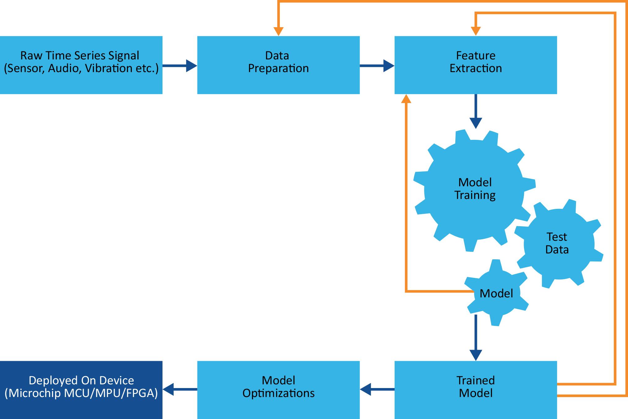
Figure 1 – The development of ML/AI models is an iterative process.
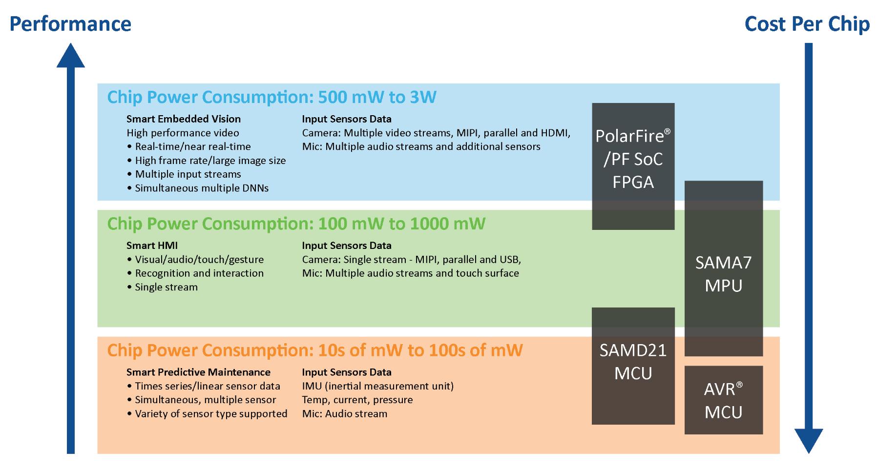
used.
With an optimized dataset and compact model, a suitable MCU can be targeted. In this respect, frameworks exist to make this easier. For example, the TensorFlow framework/flow allows for picking a new TensorFlow model or retraining an existing one. This can then be compressed into a flat buffer using TensorFlow Lite Converter, loaded onto the target and quantized.
ML and AI use algorithmic methods to identify patterns/trends in data and make predictions. By placing the ML/AI at the data source (the edge), applications can make inferences and take actions in the field and in real time, which makes the overall system
more efficient (in terms of performance and power) and more secure.
Thanks to the availability of suitable hardware, IDEs, development tools and kits, frameworks, datasets and open-source models, engineers can develop ML/AIenabled, edge-processing products with relative ease.
These are exciting times for embedded systems engineers and the industry as a whole. However, it is important not to overengineer. Much time and money can be spent developing applications that target chips with more resources than necessary, and which therefore consume more power and are more expensive.


For decades, open source software has been the quiet engine of modern computing. Every mobile app, enterprise system, and AI framework depends on it. But as global demand for software infrastructure grows, a hard truth is becoming unavoidable: open source is not free.
A new joint statement,“Open Infrastructure Is Not Free: A Joint Statement on Sustainable Stewardship,” signed by some of the most influential organizations in open source — including the Python Software Foundation (PyPI), Rust Foundation (crates.io), Eclipse Foundation (Open VSX), OpenJS Foundation, OpenSSF, Packagist (Composer), Ruby Central (RubyGems), and Sonatype (Maven Central) — warns that the very infrastructure underpinning the world’s software ecosystem is becoming unsustainable.
Most developers never think about the infrastructure that sits behind a simple npm install, pip install, or cargo build. Public package registries such as Maven Central, PyPI, crates.io, RubyGems, Composer, and Open VSX have become digital plumbing —
foundational systems that make code sharing and reuse possible at a planetary scale.
These registries serve billions of downloads each month. They are used by every major enterprise, startup, and cloud platform. Yet, despite their importance, they are mostly maintained by small nonprofit foundations and volunteer contributors.
The open letter puts it bluntly: “Billion-dollar ecosystems cannot stand on foundations built of goodwill and unpaid weekends.”
Historically, open source infrastructure has operated on goodwill and donations. Some registries are supported by corporate sponsors — GitHub
maintains npm, Microsoft backs NuGet, Sonatype funds Maven Central — while others rely on nonprofit foundations that depend on grants and sponsorships to pay for servers, bandwidth, and staff.
But the consumption model has changed. Continuous integration (CI) pipelines, automated dependency scanners, container builds, and now AIdriven development systems generate enormous volumes of automated requests — often without caching or throttling. These commercial-scale workloads, largely operated by private companies, impose heavy costs on infrastructure that was never designed for such intensity.
The letter warns of a dangerous imbalance: “A small number of organizations absorb the majority of infrastructure costs, while the overwhelming majority of large-scale users — including commercial entities that generate demand and extract economic value — consume these services without contributing to their sustainability.”
The result is a global software ecosystem resting on what the signatories call a “dangerously fragile premise.”
In the early days of open source, publishing a library meant uploading a tarball to a website. Today, expectations are radically different. Package registries are expected to offer instant global distribution, signed and immutable publishing, zerodowntime availability, and real-time security response.
Governments and enterprises now demand continuous monitoring, traceability, and auditability of open source systems — requirements that come with real costs in bandwidth, computing power, and human expertise.
Yet, the illusion of “free and infinite” infrastructure persists. Automated systems pull terabytes of packages, often redundantly, as if network bandwidth, compute, and security response were infinite public goods.
As the letter states,“The illusion of ‘free and infinite’ infrastructure encourages wasteful usage.”
One of the most striking dynamics is how public open source registries are increasingly being used to distribute proprietary software. SDKs, closed-source libraries, and commercial frameworks are often packaged and distributed through the same public channels as community-driven projects.
From a practical perspective, this makes sense: it gives publishers access to a fast, trusted, and globally replicated content delivery network already embedded in developer workflows. But it also means that public infrastructure — built and maintained for open source — is now serving as a free global CDN for private products.
As the letter acknowledges, this isn’t inherently wrong, but it does highlight a misalignment between who benefits and who pays. If open infrastructure now serves both open and commercial ecosystems, expectations and incentives must evolve accordingly. “Commercial-scale use without commercial-scale support is unsustainable.”
The Eclipse Foundation’s Open VSX Registry illustrates this imbalance vividly. Launched in 2022 as a vendor-neutral alternative to the Visual Studio Marketplace, Open VSX now handles over 100 million downloads per month. It underpins the plugin ecosystems of fast-growing developer tools like Cursor (valued at $9.9 billion), Windsurf ($1.3 billion), StackBlitz ($700 million), and GitPod (Ona, ARR $4 million).
Yet, since launch 3,342 issues have been reported by 2,504 users, 1,165 pull requests have been submitted — but only by 43 contributors, and the majority of those contributors are unpaid volunteers.
In other words, infrastructure supporting companies worth tens of billions is sustained by a few dozen unpaid individuals.

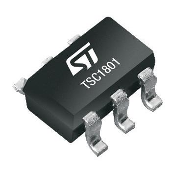
TheTSC1801isahigh-bandwidthcurrent-senseamplifierfeaturingintegratedresistors, designedforprecisepulse-by-pulsePWMcurrentcontrolintelecominfrastructure powerconversion.Itsupportswidevoltageandtemperaturerangeswithindustrialand automotiveversions.
KEYFEATURES
• Widesupplyvoltagerange:2.0to5.5V
• Fixedgain:20V/V
• Totaloutputerror<0.5%
• Offsetvoltage:±200μVmax
• Gainerror:0.1%max
• Bandwidth:2.1MHz
KEYBENEFITS
• Totalerrorguaranteed
• Reducedbillofmaterial
Needmorelow-sidecurrent-senseamplifier? Exploreourselectionofcutting-edge currentsensingsolutions

That reality, the open letter argues, should give everyone pause.
This imbalance isn’t limited to one ecosystem. A 2024 Harvard study,“The Value of Open Source Software,” estimated that the supply-side value of widely used open source software is around $4.15 billion, while the demand-side value — the value captured by users — exceeds $8.8 trillion. Even more striking: 96% of that value comes from the work of just 5% of open source developers.
The same study concluded that without open source, organizations would need to spend 3.5 times more on software to replicate equivalent functionality.
This is the paradox of open source at scale: its success has made it indispensable, but also invisible — and in many cases, unaccounted for in the budgets of those who rely on it most.
The letter is not a protest; it’s a plan. The signatories call for “practical and sustainable approaches that better align usage with costs.” Among the ideas:
• Commercial partnerships that scale funding in proportion to usage.
• Tiered access models — keeping public access free for individuals and small projects while offering enhanced performance or reliability to large-scale consumers.
• Value-added services such as detailed usage analytics for enterprise users.
None of these proposals aim to restrict access. As the letter emphasizes,“Sustainability is not about closing access; it’s about keeping the doors open and investing for the future.”
The call to action is clear: the sustainability of open source infrastructure cannot continue to depend on a small group of donors and unpaid maintainers. What’s needed is a cultural shift — from silent dependence to shared responsibility.
Organizations that depend on open source at scale are urged to:
• Engage with foundations to understand operational realities and needs.
• Audit their own usage, implementing caching and traffic reduction measures.
• Support financially, through sponsorships, memberships, or direct employment of maintainers.
Awareness is not enough.“These systems will only remain sustainable if those who benefit most also share in their support.”
The stewards behind this statement — from the Python, Rust, and Eclipse Foundations to Sonatype and the OpenJS Foundation — are not predicting collapse. They’re issuing a timely warning.“This is not (yet) a crisis,” they write.“But it is a critical inflection point.”
The message is not about turning open source into a pay-to-play model. It’s about acknowledging that sustainability requires investment — and that the world’s digital foundation cannot be maintained indefinitely by goodwill alone.
If action is taken now — through partnership, collaboration, and responsible participation — the open ecosystems that power modern computing can remain strong, secure, and open to all. If not, the cracks in the foundation will only grow deeper.
Because the truth is simple, and long overdue for recognition: Open source is not free.


Sylvain Fidelis STMicroelectronics
EEPROM is a proven non-volatile memory technology with key advantages for modern applications. Sylvain Fidelis of STMicroelectronics highlights its core strengths and why it remains the preferred choice for engineers today and in the future.
With almost 40 years since its first product development, EEPROM remains the designer’s preferred non-volatile memory (NVM) in many new designs. Chosen in applications that demand bytelevel granularity, high power efficiency, extended read/write cycle life, and long data retention, EEPROM is easy to use and brings great flexibility and scalability.
Moreover, recent innovations such as Unique ID (UID) EEPROM and Page EEPROM enhance support for current design trends such as AI edge processing, brand protection, and sustainability.
In general, EEPROM manufacturers continue to advance the technology and refine the production processes, continually increasing storage density, read/write performance, and power efficiency, as well as quality and reliability.
Today’s designers can choose from a rich selection of NVM types that offer diverse strengths. These
include the high speed of discrete serial NOR Flash, bill-of-materials savings thanks to embedded Flash in microcontrollers, and the very fast writing of FRAM (ferroelectric RAM).
On the other hand, EEPROM’s byte-write granularity is a key characteristic that stands out in comparison with these alternatives, ensuring superior performance for tasks such as data logging. In smartphones, where designers face extreme space constraints and EEPROM emulation in embedded Flash appears the best for storing data and parameters, this granularity secures EEPROM’s place on the board. In addition, low power consumption meets the needs of battery-operated applications like smart sensors, smartwatches, smartphones, health and fitness trackers, and other wearables.
Additionally, by offering extended read/write cycle life and long data retention, EEPROM delivers the extreme reliability needed to fulfill datalogging needs in automotive applications. Typical uses include storing important parameters for the application to use and recording digitalized
information from multiple sensing channels in automated driving systems. With data retention of 100 years or more, EEPROM can easily guarantee performance throughout the lifetime of the vehicle.
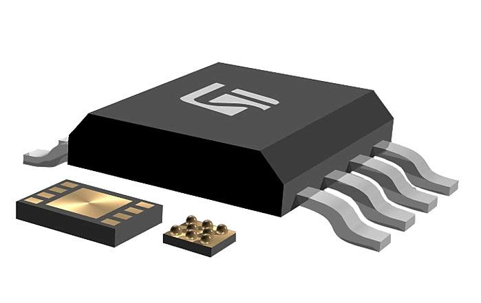
Designers also appreciate the flexibility that EEPROM allows during system development. Memory requirements can be difficult to predict when the project starts and are usually expected to increase significantly as the design progresses. Serial EEPROMs of various densities can share a common package type and pinout, which lets storage scale easily by choosing a device of higher capacity without changing the board layout. Manufacturers offer ICs of various densities, from low-cost 1Kbit devices to 4-Mbit, and more in popular 8-pin surface-mount SO-8 and various other packages. Finalizing a design for production is barely more complicated than sending instructions to the purchasing department.
Two important recent developments show how EEPROM is adapting with the priorities of the modern world, particularly the demands of edge AI applications, protection for brands and consumers against product counterfeiting, and sustainability concerns that highlight the virtues of repairable electronics.
consistently increased, the users of electronic devices having a growing appetite for more data and for more accurate product settings. In the 2000s using an EEPROM above 256-Kbit looked unthinkable, as did using a 2-Mbit in the early 2020ss. The value proposition of Serial EEPROMs is that developers need only allocate a small 8-pin package to data storage in their application and then have the flexibility to select any memory density.
By introducing Page EEPROMs, ST has broken the glass ceiling by being able to fit up to 32-Mbit of reliable data storage in a small 8-pin package.
Page EEPROM is an innovation by STMicroelectronics. It primarily targets applications that need the storage capacity and speed of Flash –particularly its ability to handle over-the-air (OTA) firmware updates quickly and efficiently – with EEPROM’s power efficiency and durability. Suited for smart meters, which demand extremely low power, byte-level data logging, and small size, it’s also just right for data-hungry edge-AI devices. Typical applications here include industrial sensors for applications such as asset tracking and intelligent condition monitoring, e-bikes, and healthcare devices. Some of the first applications for this novel hybrid memory were in behind-the-ear hearing aids and GPS trackers.
Over the past 40 years, the amount of data stored in our customer applications has relentlessly and
When introduced in 2024, Page EEPROM was available with storage densities of 8 Mbits, 16 Mbits, and 32 Mbits. The devices support byte-
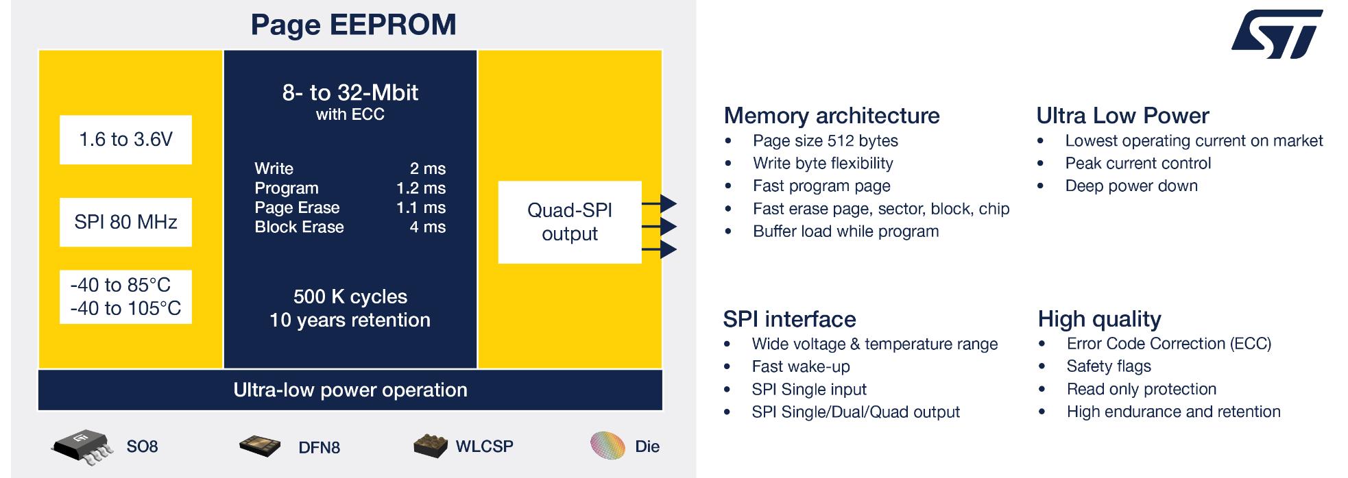


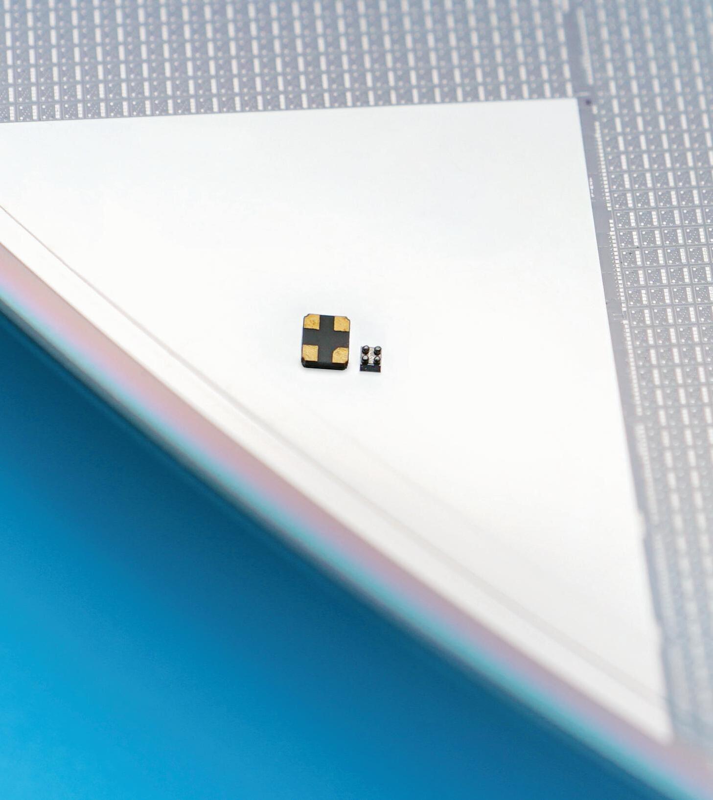
level write operations, which makes them perfect for data logging, while page/sector/block erase and page programming facilitate Over The Air (OTA) firmware management. In addition, buffer loading optimizes initial programming.
The data-read speed, at 320 Mbit/s, is faster than standard EEPROM and comparable with serial NOR Flash. On the other hand, write-cycle endurance of 500,000 cycles is several times higher than conventional serial Flash and data retention is 100 years. Also, the overall demand on the battery can be 10 times lower. While write current is at the same level as many conventional EEPROMs, there is also a deep power-down mode with fast wakeup that reduces the current to below 1 µA.
A further, novel feature of these devices is the peakcurrent control that restricts the maximum consumption to below 3 mA. This effectively stabilizes the power consumption and minimizes power supply noise, while in principle allowing smaller batteries and longer runtimes.
Unique ID EEPROMs contain a 128-bit read-only unique identity (UID) that’s pre-programmed when the device is manufactured and then permanently locked. Since the ID cannot be changed, OEMs can use this feature like an entry-level secure element to provide basic product identification and clone detection. The UID also permits traceability which, in turn, allows accurate product-reliability analysis and can simplify re-use and repair of equipment to support sustainability goals.
The UID is provided in addition to conventional EEPROM user-memory space, with up to 2-Mbit available for parameter storage and data logging. Reliability is assured, with write endurance of four million cycles and data retention of 200 years, and power consumption is extremely low. The devices also support I2C communication up to 1MHz fastmode plus and allow random and sequential read modes while providing a write-protect mode for the entire memory array.
The overall global market is valued at about $800 million annually. STMicroelectronics began producing EEPROM ICs in 1987 and is currently the world’s largest supplier; a position held since 2005. In total, the Company has shipped about 44 billion devices to date and has a portfolio that contains over 400 different part numbers including UID and Page EEPROM ICs. The many different variants offer the widest portfolio of storage density and package options, performance parameters, and temperature grades on the market, as well as support for standard operating voltages from 1.2V to 5V, supporting high-volume trends.
All devices benefit from ST’s product longevity program, which ensures availability of commercialand industrial-grade EEPROMs for 10 years, and 15 years for automotive-grade devices. The Company’s IDM (integrated device manufacturer) model gives control over all stages of the product lifecycle, including design, production, and marketing. Close in-house cooperation helps deliver reliable products more quickly and drives product and process development based on real customer feedback.
As EEPROM technology has evolved, the typical bitcell area is now more than 500 times smaller than the first-generation architecture, while memory density has increased by 1,000 times on the same die size. Endurance is also greatly increased, with the toughest devices achieving 4 million cycles and ensuring zero-failure data retention.
EEPROM continues to offer a strong value proposition, alongside Flash technologies and FRAM, in applications that need robust and reliable, highperformance NVM. While recent innovations bring important new capabilities, ongoing technological development further extends EEPROM’s underlying attributes. In today’s AI-centric, sustainabilityconscious world, the latest EEPROMs are ready to meet the needs of engineers targeting new designs. More info at www.st.com/eeprom


DK Singh Renesas Electronics
From the outside, an electronic system may seem like a single unified discipline or device that works as one. But under the hood lies a different reality: a fragmented, multilayered world where each layer is so independently complex that it spawns its own ecosystem of tools, experts, workflows, and even philosophies.
And in this layered chaos lies both beauty and challenge: It’s an Orchestra without a conductor:
Each layer operates like an independent discipline and advances at its own pace, following its own innovation curve. In semiconductors, we’ve pushed boundaries to the brink of physics—etching features at the
1nm scale, leveraging EUV lithography, and packing billions of transistors into a fingernail-sized die. Meanwhile, in PCB design, the very layer that connects these marvels—the progress has been far more incremental. We still wrestle with trace widths, impedance control, and manufacturability limits that haven’t evolved nearly as fast.
The depth and pace of innovation within each layer is staggering, yet coordination between them remains minimal.
This independence, while enabling deep specialization, also creates silos. It's rare to find an engineer—or even a company—that fully grasps all layers end-to-end. And this is not due to a lack of effort, but because each layer is a universe in itself. The asymmetry in advancement is not due to lack of effort. It’s a symptom of deep specialization and specialization leads to silos.
Over the past two decades, I’ve had the rare opportunity to experience this complexity firsthand—from system design in Japan to Silicon development & system integration in the U.S.A., and now at the intersection of AI and embedded design. Each chapter of my career brought me face-to-face with a new layer.
What struck me wasn’t just the depth of each domain—but how unaware each layer often was of the others. The analog designer rarely interacted with the embedded software engineer. The PCB layout specialist seldom had full context on application-level behavior. And system-level decisions were often made without end-to-end visibility.
Experience has thought me that the fragmentation in embedded electronics is not accidental—it's structural by design
1. Semiconductor Devices (The Foundational Layer): Microcontrollers, SoCs, memory, sensors, power ICs, specialty chips, passives. Device physics, process technology, chip architecture, IP blocks. This layer itself is a multilayered structure.
2. Architecture & Circuit Design: The Design layer that shapes the system, Analog/mixedsignal design, power trees, clock & signal
conditioning, Component selection & design trade-offs, schematic capture.
3. Simulation, Verification & Validation: Prefabrication simulation, Predictive modeling, signal integrity analysis, thermal/EMI simulation, bench testing
4. PCB Design & Physical Integration:
Implementation layer where the orchestra is played, physical constraints, trace geometry, via structures, thermals, manufacturability.
5. Embedded Firmware & Real-Time
Software: The invisible layer that brings HW to life, Real-time control, hardware abstraction, drivers, bridging HW and FW, debugging,
6. System Integration & Toolchain
Automation: The glue layer where FW, HW and applications meet reality. Bridging core HW, FW and system subblocks, testing pipelines & flow
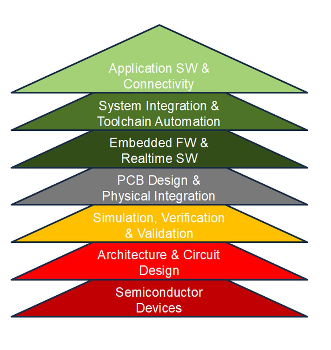
The multilayered world of embedded electronics: each layer forms its own ecosystem, advancing independently yet rarely in full harmony.
Renesas Electronics Corporation and Altium have announced Renesas 365, Powered by Altium, a pioneering solution set to redefine how modern electronic systems are conceived, designed, and managed. The launch marks a major milestone following Renesas’ acquisition of Altium, combining deep semiconductor expertise with a leading cloudnative design platform.
Renesas 365 integrates hardware, software, and lifecycle management into a single digital environment, eliminating inefficiencies and enabling continuous system context. By uniting Renesas’ comprehensive portfolio of embedded compute, analog, connectivity, and power solutions with Altium’s collaborative cloud tools, the platform addresses critical industry challenges such as manual component searches, fragmented documentation, and siloed teams.
Built on five pillars—Silicon, Discover, Develop, Lifecycle, and Software—Renesas 365 ensures that every design is optimized for performance,
collaboration, and security. Engineers can rapidly discover complete system solutions, develop within a real-time collaborative environment, and maintain persistent digital traceability across the product lifecycle. Advanced features include AI-ready development tools, over-the-air (OTA) updates, and compliance tracking to meet the demands of software-defined products.
By bridging the gap between silicon and system-level design, Renesas 365 accelerates time to market, empowers smarter decision-making, and sets a new industry standard for electronics system development. The platform is expected to be available commercially in early 2026.
For more information visit the Renesas 365 website
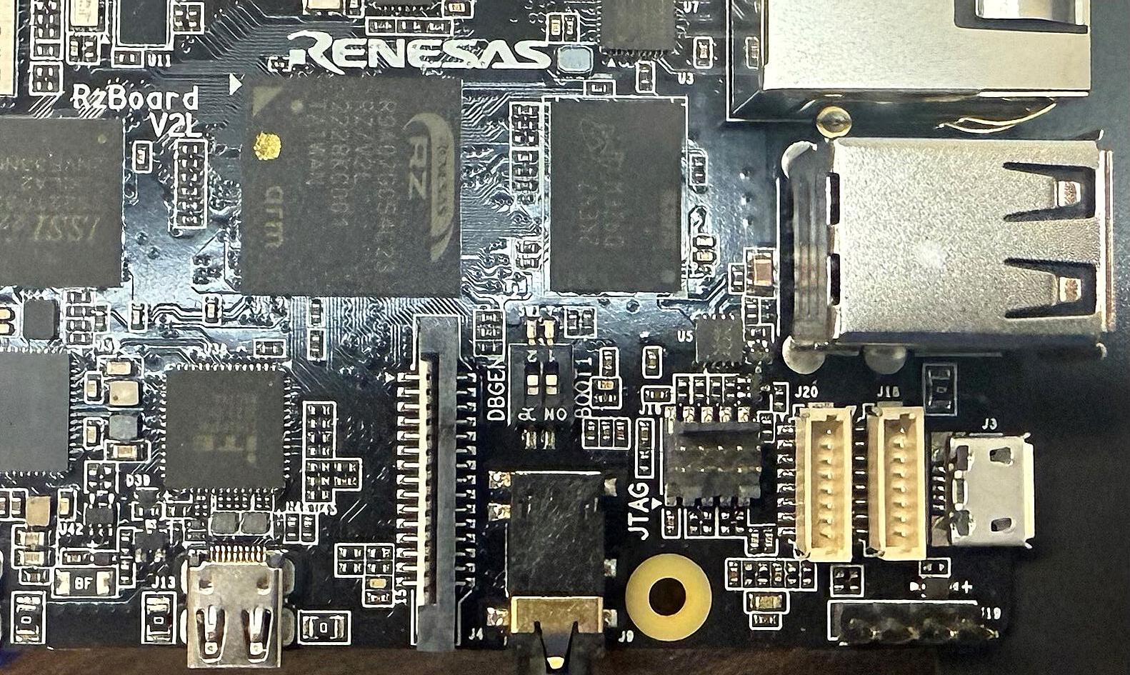
A printed circuit board (PCB) brings semiconductor devices, connectors, and power management into physical reality—one of the many layers in the fragmented ecosystem of embedded electronics.
7. Application Software & Connectivity: The user facing bridge between machines and humans. Use case and user interface, data analytics, cloud integration, mobile apps, remote control, Communication protocols, latency management, UX design
The Consequence: Fragmentation by Design: This separation is not accidental. It is the result of necessity.
Each domain has grown so deep and fast that cross-layer mastery is nearly impossible. Consequently:
• Toolchains remain isolated, leading to inefficiencies in integration and debug.
• Expertise becomes domain-locked, with few engineers able to collaborate across layers.
• Design cycles suffer delays, as insights from one layer are lost in translation across others.
In short, the embedded electronics industry is rich in capability but fractured in execution.
The next leap in embedded systems, a true system-level co-design, rapid prototyping, and AI-assisted development, will come from connecting these independent ecosystems. Not by flattening their complexity, but by creating shared abstractions, interoperable tools, and design frameworks that allow each expert to work in harmony without mastering every detail.
Until then, we’ll remain in a world where brilliant minds work in parallel, yet rarely in unison. It’s an opportunity.


Piyush Sevalia SiTime
SiTime’s Titan Platform MEMS resonators are transforming the $4B resonator market with solutions up to seven times smaller than quartz, yet tougher, more power-efficient, and easier to integrate. From wearables to medical implants, IoT, and Edge AI, Titan unlocks new possibilities for device makers to design smaller, smarter, and more reliable products.
SiTime has long been known as a semiconductor company that provides high-quality, silicon-based timing solutions that utilize Micro-ElectroMechanical Systems (MEMS) technology. These solutions, which have traditionally been dominated by a wide range of oscillators and clocks designed to replace traditional quartz products, has now grown to include a new breed of resonator, the Titan Platform™ MEMS resonator family.
These new MEMS resonators complete SiTime’s comprehensive timing portfolio, offering customers a revolutionary solution that's 2-3 generations smaller than quartz alternatives while delivering superior power performance, reliability, and
integration flexibility. This is the company’s first entry into the $4B global resonator market and transforms the company into the only supplier covering all three major categories of timing products – oscillators, clocks and now resonators.
The Titan Platform MEMS Resonator is a major advance for the developer community with SiTime now enabling a vast range of new design possibilities for small, battery-powered, connected devices that will power the next generation of wearable, medical, smart home and industrial IoT devices and more.
The key to the Titan Platform MEMS resonator’s success is in its ability to overcome limitations inherent in quartz resonators’ larger size, integration difficulties, and limited resilience to environmental stressors.
Taking size as the first example, what is immediately striking is the drastic reduction in footprint. It is at least four times smaller - and in the case of 32 MHz at least seven times smaller - than its quartz counterparts. This unprecedented level of miniaturization enables designers to create substantially smaller devices, which is essential for next-gen wearables like smartwatches, fitness rings, hearing aids and medical implants, to name a few.
The advantage of space savings is that it makes substantial amounts of precious board real estate available so engineers can readily add new features, functionality, sensors, or longer-lasting batteries on an existing board without having to resort to a larger one.
Innovative use of the newly available space, coupled with new and enhanced functionality enables the Titan Platform to provide two flexible implementation paths that simplify the design process and enable new levels of integration.
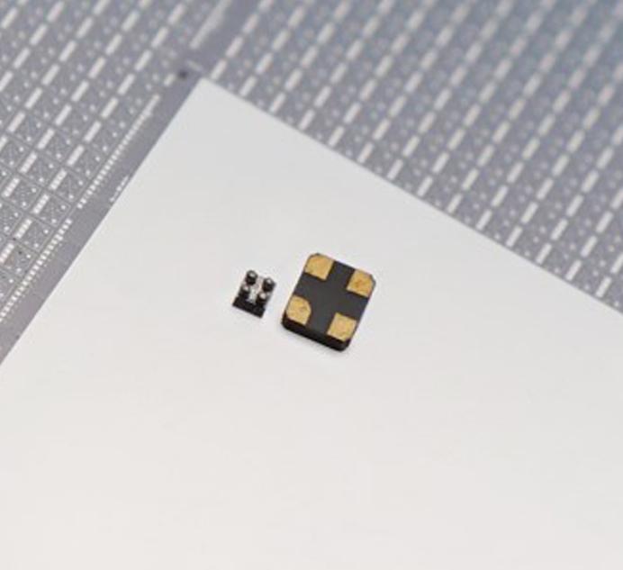
Titan with 1210 size Quartz Resonator which is 7x larger.
As a start, its bare die co-packaging with SoCs/MCUs is a genuine game-changer. This allows the resonators to be integrated directly within the same package as the System-on-Chip (SoC) or Microcontroller (MCU), eliminating the need for a discrete resonator component on the PCB. This means that there is far less design complexity, less design effort during end product development, diminished manufacturing costs, and far fewer potential points of failure.
Alternatively, for designs where direct co-packaging isn't feasible or desired, the ultra-small form factor of the Titan Platform still allows for easy PCB mounting, taking up a fraction of the PCB space compared to a quartz crystal.
This ease of direct integration is especially beneficial for SoC and MCU makers because they can now deliver a more complete and unique timing design solution to their customers, increasing the value of their products while boosting their revenue.
Beyond space efficiency, the Titan Platform delivers significant performance improvements that enable more robust and efficient devices to be created. This is in part due to improved battery life.
With a reduction in oscillator circuit power by as much as 50%, along with three times faster startup, the resonators deliver extended battery life for power-conscious devices. This means, for example, that devices like fitness rings with tiny rechargeable batteries can power on, quickly transfer data and return to a low-power state in a fraction of the time previously required, extending their battery life.
And let’s not forget durability and stabilitytraditional quartz crystals are fragile. The MEMS resonators have been tested and verified to provide up to 50 times better shock and vibration resilience, making them virtually indestructible in harsh environments. This is essential for industrial IoT, asset tracking, and a wide variety of other devices that must operate reliably under challenging environmental conditions.
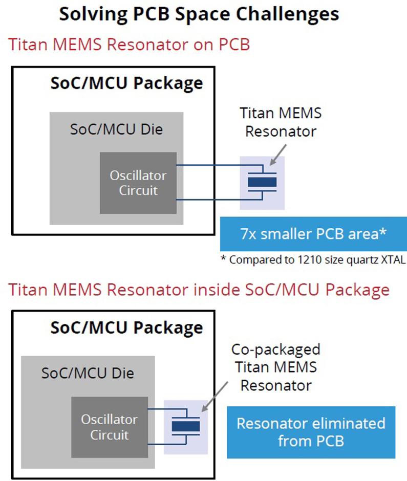
Titan MEMS resonators free up precious PCB space by being up to 7× smaller than quartz alternatives—or by being copackaged directly inside the SoC/MCU, eliminating the need for a discrete resonator on the board.
This durability includes stability under extreme temperatures. The resonator maintains tight frequency stability from40°C to 125°C and boasts up to five times better aging stability over a period of five years. Quartz alternatives typically only specify aging after one year and at 25°C, which means that by the time the crystal is mounted on the board the aging budget may already be nearly exhausted due to time elapsed since production. Titan resonators’ superior stability and aging performance ensures consistent and accurate timing, which is critical for the long-term reliability of connected devices.
These advancements collectively empower designers to push the boundaries of what's possible in terms of device size, power consumption, functionality, and ruggedness, driving innovation in Edge AI applications and beyond.
For SoC/MCU makers in particular, Titan enables true integration by co-packaging the resonator inside chip packages.
It also eliminates the need to select/qualify quartz resonators, optimize PCB placement, or manage trace coupling, which in turn avoids delays – often of several weekscaused by having to send boards back to quartz suppliers for validation.
All of this creates new revenue-generating opportunities for semiconductor partners who can produce higher-value chips and expand into differentiated offerings.
All these benefits accrue to end customers at each stage. For example, SoC vendors can now offer complete solutions to their customers with an increased ASP potential due to integrated value delivery. The customer experience itself is improved because it’s much simpler, i.e., there is no longer any need to hunt for resonators that match to the specifications of a particular SoC. All of this results in much faster time to market which is vital in a highly-competitive, rapidly-evolving market.
As already suggested, system designers can use the extra space afforded by Titan to include new features or larger batteries; and the simplified designs significantly reduce the component count and, thus, manufacturing costs. All in all, Titan empowers the creation of more advanced, reliable and innovative products across wearables, medical devices, Industrial IoT, smart home, Edge AI and beyond –accelerating their path to market.
The way that SiTime has differentiated Titan’s MEMS technology from traditional quartz crystal technology ensures that

Titan MEMS resonators empower designers to push the boundaries of what's possible in terms of device size, power consumption, functionality, and ruggedness, driving innovation in Edge AI applications and beyond.
semiconductor manufacturing can now be done with consistent quality and reliability. The use of MEMS die-level vacuums that enable plastic package integration thereby simplifying system design is truly a gamechanging innovation.The emergence of Titan has turned SiTime into a one-stop timing
solution provider as it is now the only company with a complete timing portfolio. SiTime is not just a parts supplier, it works closely with its customers to understand their unique challenges and enable them to produce cutting-edge new products.

Titan is built on SiTime’s sixth-generation MEMS technology, FujiMEMS™, delivering unmatched performance and reliability compared to legacy quartz resonators:
• Smallest size: 0505 CSP (0.46 x 0.46 mm)—7x smaller PCB area than 1210 quartz, 4x smaller than 1008 quartz.
• Up to 50% lower oscillator circuit power.
• Up to 3x faster startup with 3x lower startup energy.
• Up to 5x better aging stability and specified for 5 years at the maximum temperature.
• Tighter stability across wide temperature ranges up to –40°C to 125°C.
• Up to 50x better shock and 50x better vibration resilience.
• Titan SiT11100 (32 MHz): production samples available now.
• Titan SiT11101 (76.8 MHz), SiT11102 (38.4 MHz), SiT11103 (48 MHz) and SiT11104 (40 MHz): engineering samples will be available starting December 15, 2025.
For more information, please visit: https://www.sitime.com/products/resonators/mhz-mems-resonators

Investment and Development Agency of Latvia (LIAA)

Latvia has steadily captured the attention of Finnish entrepreneurs – not just as a nearby market, but as a genuine partner in growth and innovation. With its skilled workforce, strategic location, and increasingly favourable investment climate, Latvia is emerging as one of the most promising destinations for Finnish business expansion in the Baltics and beyond.
Finland is among Latvia’s most important economic partners, ranking as the fifth-largest import partner and ninth-largest export destination in 2023. By the end of that year, Finnish companies had invested a total of €214.8 million in Latvian equity across almost 300 firms – a clear signal of trust and longterm interest. Finnish-owned companies now operate in a wide range of sectors, from logistics and manufacturing to IT and construction.
DEFENCE, DIGITAL, AND GREEN ENERGY DRIVE FINNISH INVESTMENT
One of the clearest indicators of this close relationship is the physical presence of Finnish industry in Latvia. The Patria Latvia

joint venture in Valmiera, part of the Common Armoured Vehicle System (CAVS) programme, is a flagship example. The facility assembles Patria 6×6 armoured vehicles for domestic and export markets, strengthening both countries’ defence capabilities while creating skilled jobs and transferring high-value manufacturing knowhow.
Beyond defence, cooperation in innovation and technology is gaining momentum. Helsinki-based DataCrunch Oy, for instance, has partnered with Latvia in submitting a conceptual proposal to the European Commission for an AI GigaFactory – a major project aimed at developing secure, energyefficient computing infrastructure for Europe’s sovereign AI needs. If realised, the initiative would not only strengthen Europe’s technological independence but also highlight Latvia’s role as a digital hub capable of hosting high-impact infrastructure powered by renewable energy.
According to DataCrunch’s representative, Consortium Coordinator Michael Champion, the AI GigaFactory project is currently in a preliminary stage, as the EU has yet to
release the final call. He says the company is hopeful that the proposal will go through:
- We would like to see a facility in Latvia, and we are quite open that we ultimately want to have a Baltic–Nordic consortium built.
He explains some of the reasons why DataCrunch chose Latvia for this initiative:
- We’re committed to running our data centres on 100% renewable energy, and Latvia – already fourth in Europe for renewable generation in 2023 – is only increasing its capacity. It’s an ideal mix for us: strong green energy, excellent digital and power infrastructure, and a good regional balance. We can’t have everything in Finland, so expanding to Latvia makes sense both for energy availability and for building a distributed, resilient network in a market that’s still largely untapped for AI data centres.
These developments are not isolated success stories – they are part of a broader trend of

Finnish companies choosing Latvia as their base for manufacturing, services, and technology development. The reasons are both practical and strategic. Latvia’s geographic position at the crossroads of the Nordics, Western, and Eastern Europe offers unmatched connectivity – by air, sea, and land. Finnish and Latvian economies are naturally complementary: Finland’s strong industrial base and R&D capabilities align well with Latvia’s cost-competitive, agile, and innovation-driven environment.
Moreover, the Latvian government is actively fostering a pro-investment climate. In 2025, it approved a national plan to attract foreign investment and improve access to finance, with the goal of increasing total FDI from €22.5 billion to €32 billion by 2029. In just the first half of 2025, nine new investment projects worth €156 million were confirmed, creating more than 500 new jobs. LIAA’s dedicated support for foreign investors –including Finnish companies – ensures smooth entry, local partnership facilitation, and access to incentives for high-value projects.
Latvia’s cost advantage remains another draw. Business operational costs are significantly lower than in Finland, allowing companies to increase margins and scale operations efficiently. Yet, the quality of infrastructure, digital readiness, and workforce skills remain high – factors that
have consistently placed Latvia among the EU’s top countries for digital public services and internet connectivity.
Culturally and geographically close, Finland and Latvia share more than a border across the Baltic Sea – they share an outlook on innovation, sustainability, and pragmatic business growth. Gatis Ozoliņš, Head of the LIAA Representative Office in Finland, notes that it is already straightforward for Finns to do business with Estonia, but Latvia is still largely untapped by many Finnish companies. He shares his insight:
- Finnish companies that have established their production facilities or businesses in Latvia are usually very happy with their decision. They see that the Latvian mentality is quite similar to their own, and they benefit from strong government support. In smaller countries like Latvia, the government works closely with businesses, whereas in larger countries there tends to be a wider gap between companies, officials, and politicians.
For Finnish companies exploring where to expand next, Latvia offers a blend of opportunity, stability, and proximity that is hard to match. It is not just a convenient neighbour – it is a gateway to scalable growth in Europe.

For more information contact
Gatis Ozoliņš: gatis.ozolins@liaa.gov.lv (Finland)
Valters Jēkabsons: valters.jekabsons@liaa.gov.lv (Sweden)

The article was financed with the support of the Recovery and Resilience Facility –NextGenerationEU. The views and opinions expressed are solely those of the author(s) and do not necessarily reflect the views of the European Union or the European Commission. Neither the European Union nor the European Commission can be held responsible for them.


The world of embedded solutions is expanding rapidly, but navigating the best way to find them can be a challenge. What is the right approach for your project? What is the relationship between component suppliers and distributors?
Embedded Conference Finland is the only independent professional event focusing on embedded technology. ECF is designed for electronics designers seeking the latest advancements, corporate buyers aiming to streamline their supply chains, business leaders driving innovation in their companies, and anyone passionate about embedded electronics!
The event is free for visitors. ECF26 is planned for May 2026.
For more information see www.embeddedconference.fi
To book a place or ask for sponsor packages please contact
ETN editor-in-chief Veijo Ojanperä vo@etn.fi
+358-407072530 or Sales manager Rainer Raitasuo
+46-734171099
rr@etn.se
ETNdigi is a specialized digital magazine from ETN. We cover components, test & measurement, radios & networks, and the entire scope of embedded software. To put it simply: everything related to electronics and embedded design.
Want to join us? Just contact ETN editor-in-chief Veijo Ojanperä at vo@etn.fi or our sales manager Rainer Raitasuo at rr@etn.se. More info about the pricing can be found at etn.fi/advertise.