

JUNE 2023 The factors of accurate measurements Page 12 Automate double-pulse testing in WBG devices Page 22 Measurements verify power integrity Page 24 measurement TEST & handbook A SUPPLEMENT TO DESIGN WORLD


Many, if not most, design engineers use bench test equipment — oscilloscopes, multimeters, spectrum analyzers, function generators, and so on. Test doesn't, however, end at your bench; it goes onto the production floor. In production, test is about making sure that the manufacturing process operates within tolerances. That is, if the product is built correctly, it should pass production tests.
That's the big change we've brought to the 2023 Test & Measurement Handbook. We've added articles relating to production and manufacturing test for systems and subsystems. So far, we haven’t touched on semiconductor test, but we might just do that online over the coming year.
Test engineers have different priorities than design engineers. For example, test engineers must consider throughput, costs of test, automation, and footprint. Throughput relates directly to the cost of test. If your facility produces, say, thousands of products every day, throughput needs to be as quick as possible. To achieve high throughout, you need to automate the process of applying test signals to your DUT and measuring the results. That means software: test executives, test routines, instrument drivers, databases, test reports, and the like. Furthermore, test systems need to be easy to operate.
If you're not familiar with manufacturing test and need some background, look to the following articles:

· "How test executives automate equipment and processes" provides a toplevel view of test software.
· "How modularity benefits test systems" looks at automated test hardware such as PXI.
· "What is an instrument driver and why do I need one?" explains how test executives and individual test routines communicate directly with test instruments, be they modular or boxed. Chances are, you'll need both configurations in a production test station.
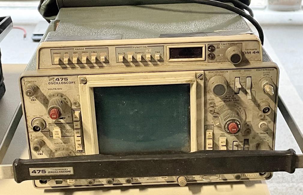
Do you work with high-speed digital signals? If you do, then you understand the importance of signal integrity. Without quality signals, bits get lost resulting in bit errors. That's something nobody wants. Power integrity, a subset of signal integrity, is the study of how power and its issues — droops, dips, ripples, and noise — affect signal integrity. Today's oscilloscopes include software written specifically for measurements on power planes. “Measurements verify power integrity” and “How to make fast and accurate powerintegrity measurements” explain why you need to measure power integrity and how to do it. While EE World focuses on modern test equipment and how to use it, we still appreciate vintage equipment. Sure, you can find all kinds of vintage test equipment online, but there's nothing quite like seeing it in person. Here's an oscilloscope I photographed at a monthly swapfest (swapfest.us) on the MIT campus in Cambridge, Mass. It needs some cleaning, and it might even still work. •


02 Editorial Test goes beyond the bench
With private networks connecting to many Iot devices, testing the device's user interface requirers updatiing test processes.

08 How Modularity benefits test systems
By understanding the key issues at every phase of the product lifecycle. ENgineers can make decisions that result in flexible, reliable, and scalable test systems. Taking a modular approach to test system development can accelerate development and mitigate risk throughout the entire product lifecycle.
12 The factors of accurate measurements
All measurements need reliable, accurate equipment that's traceable to worldwide standards. Without that, measurements have no value.

15 How test executives automate equipment and processes
Working through test-program sets and drivers, test executives let engineers prganize tests into logical sequences. They provide users interfaces for test ttechnicians and store test results for analysis.
18 Co-Packaged Optics: Promises and Complexities

Integrating optics into the same package as switching ASICs improves signal integrity and increases data rates, but challenges remain.
22 Automate double-pulse testing in WBG devices
By automating double-pulse testing of wide bandgap devices such as Sic and Gan power devices, you can cut setup and analysis time.
24 Measurements Verify PowerIntegrity Engineers should measure and analyze power integrity on the power and ground planes of a board's power distribution network. Understanding power integrity is crucial when evaluating circuit power quality because it has a direct influence on performance.
29 How to make fast and accurate power-integrity measurements
Today’s electronic devices with fast FPGAs, ASICs, and other ICs rely on ever-smaller power rail voltages with tight tolerances. Engineers who incorporate these ICs into their systems need to use oscilloscopes, probes, and measurement techniques that align with today’s tight voltage rail tolerances.
EDITORIAL
VP, Editorial Director Paul J. Heney pheney@wtwhmedia.com
Editor-In-Chief
Aimee Kalnoskas akalnoskas@wtwhmedia.com
Senior Technical Editor Martin Rowe mrowe@wtwhmedia.com
Associate Editor Emma Lutjen elutjen@wtwhmedia.com


MARKETING
VP, Digital Marketing Virginia Goulding vgoulding@wtwhmedia.com
31 Testing satellite uplink and downlink chains
Noise measurement, LO substitution, receiver stress testing, power measurement, CCDF and PAPR characterization, and antennapattern measurement play critical roles in link budget, bit-error rate, and SNR requirements.
34 Test methods for mmWave AiP designs bring tradeoffs
Engineers have several mmWave over-the-air test methods avaliable for evaluatinf phased-array antennas used in antenna-in-package designs.
38 What is an instrument driver and why do I need one?
ONLINE contents TEST & MEASUREMENT HANDBOOK • JUNE 2023
Instrument drivers take some of the sting out of controlling test measurements by adding an abstraction layer.
Digital Marketing Coordinator Francesca Barrett fbarrett@wtwhmedia.com
Digital Design Manager Samantha King sking@wtwhmedia.com
Webinar Manager Matt Boblett mboblett@wtwhmedia.com
Webinar Coordinator Emira Wininger emira@wtwhmedia.com
CREATIVE SERVICES & PRINT PRODUCTION
VP, Creative Services Matthew Claney mclaney@wtwhmedia.com
Senior Graphic Designer Mariel Evans mevans@wtwhmedia.com
Graphic Designer Shannon Pipik spipik@wtwhmedia.com
Director, Audience Development Bruce Sprague bsprague@wtwhmedia.com
DEVELOPMENT
Web Development Manager B. David Miyares dmiyares@wtwhmedia.com
FINANCE
Controller Brian Korsberg bkorsberg@wtwhmedia.com
Accounts Receivable Specialist Jamila Milton jmilton@wtwhmedia.com
WTWH Media, LLC 1111 Superior Ave., Suite 2600 Cleveland, OH 44114 Ph: 888.543.2447 FAX: 888.543.2447

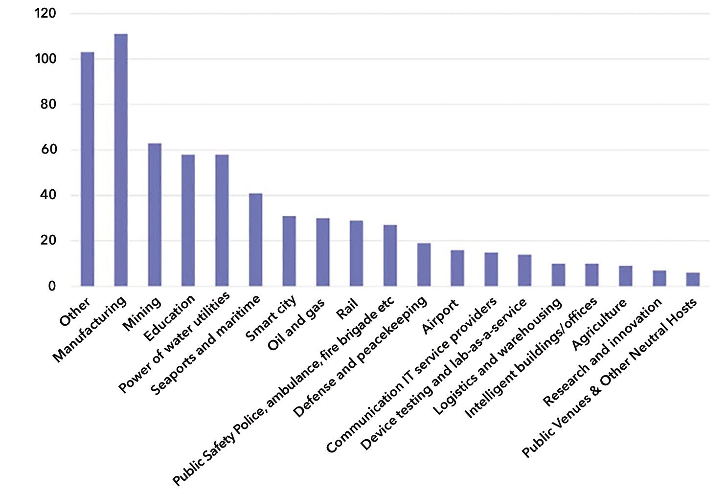
Many IoT use cases rely on private 5G networks because they offer greater network control, better security, more reliable performance, and dedicated coverage and capacity as opposed to using a public network. With these advantages, private networks play an important role in specialized use cases for vertical markets.
Based on current GSA data (Figure 1), manufacturing is the top industry vertical for private 5G, followed by mining and education. Other industries are expected to grow as long as one key hurdle—UE operation—can be overcome.
Device performance in private 5G is a challenge because, while operator and private 5G networks have similar building blocks, UE is very device-centric based on use case. Additionally, 5G introduces control user plane separation (CUPS), which enables vendors to combine RAN and core network hardware components with software from other sources. With so many varieties in vendors, testing only against 3GPP specifications compliance is not enough.
You should properly test IoT devices against different configurations and combinations and ensure the key performance indicators (KPIs) are properly measured. For engineers, understanding all elements of how users can use the UE, as well as the environments in which they are being deployed, are necessary to ensure devices meet performance parameters.
3GPP Release 16 opens doors
3GPP Release 16 paves the way to private 5G networks. It lets 5G become a substitute for private wired Ethernet, Wi-Fi, and LTE networks by including capabilities for industrial environments.
3GPP also provides standards and guidance on private 5G network deployment. Network architecture and deployment environment affect how you need to test an IoT device's UE.
The most "private" architecture is a nonpublic network (NPN), which is an enterprise with a dedicated, on-premises network. 3GPP categorizes NPNs in two ways:
· Stand-alone non-public network (SNPN): this design does not rely on network functions from a public land mobile network (PLMN). An SNPN-enabled UE must be configured with a subscriber identifier (SUPI) and credentials for each subscribed SNPN identified by the combination of PLMN ID and network identifier (NID). In addition, 3GPP Release 16 specifies the ability for
a UE to obtain PLMN services while on a stand-alone non-public RAN. This is related to when the UE has a subscription and credentials to obtain services from both PLMN and SNPN.
· Public network integrated NPN (PNI-NPN): in this model, a PLMN ID recognizes the network, while a closed-access group (CAG) ID locates appropriate cells. A CAG cell broadcasts the designated CAG identifiers per PLMN, which must be supported by UE operating on the network. Only devices that have access credentials for that specific CAG ID can latch on to such cells, thus providing access restriction.
Hybrid private 5G networks use a mix of public mobile network components and dedicated on-premises elements. UE for
With private networks connecting to many IoT devices, testing the device's user interface requires updating test processes. Adnan Khan, AnritsuFigure 1. Vertical markets implementing private 5G networks (Image: GSA).
hybrid networks has its own set of performance parameters, depending on network configuration.
Three hybrid designs exist:
· Radio access is shared with the public network; everything else is private.
· The user plane is private, but the control plane and radio access are shared.
· Network slice option; one virtual slice is dedicated to the private network while all other elements reside on a public network.
Because private 5G networks use unlicensed and shared spectrum, device integration can become complex. Systems integrators, who have become key players
Ensuring UE performance in private 5G QoS and connectivity take on an added layer of complexity in many private 5G use cases. For example, in a smart factory, there can be robots with hundreds of sensors and machinery with multiple actuators operating in an environment with considerable interference sources. Such a setting has created the need for stress testing to determine how the UE will operate under such extreme conditions.
Given the proprietary nature of many private 5G networks, the prevalence of Open RAN architecture, and data sensitivities, security is a main priority. Many UE manufacturers employ practical security testing, which uses a network
5G networks have unique requirements that are more specific and varied than open public networks. Not only are there a tremendous amount of frequency/band combinations that must be considered for "sunny-day" testing but attention needs to be given to ensure devices that are supposed to work exclusively in an NPN environment do not connect to macro networks and unauthorized UE do not connect to an NPN. For this reason, other tests must be conducted to ensure performance, including:
· Connectivity 5G IoT devices need proper testing to verify call connection, cell selection/ reselection, access control, and any mobility implications
support cellular, Wi-Fi, and short-range wireless technologies, such as Bluetooth and Zigbee. Ensuring UE can seamlessly transfer from one technology to another is essential to private 5G network performance.
· Interference: given most private 5G network use cases, interference testing is critical. In addition to supporting multiple technologies, devices must operate in less-thanideal real-world environments and in mission-critical scenarios. Engineers must have confidence product performance will not degrade due to interference before shipping to customers.
Implementing a test process to support private 5G UE requires a practical approach. The test environment must simulate realworld scenarios to efficiently verify that the UE will perform when deployed into a private 5G network. Design your test system with intuitive software to efficiently support various and ever-changing test conditions and evolving standards, which will help to control test costs.
in private 5G, must verify that UE operates according to specification, elements are integrated properly to guarantee end-to-end quality of service (QoS), and connectivity between UE and network is reliable.
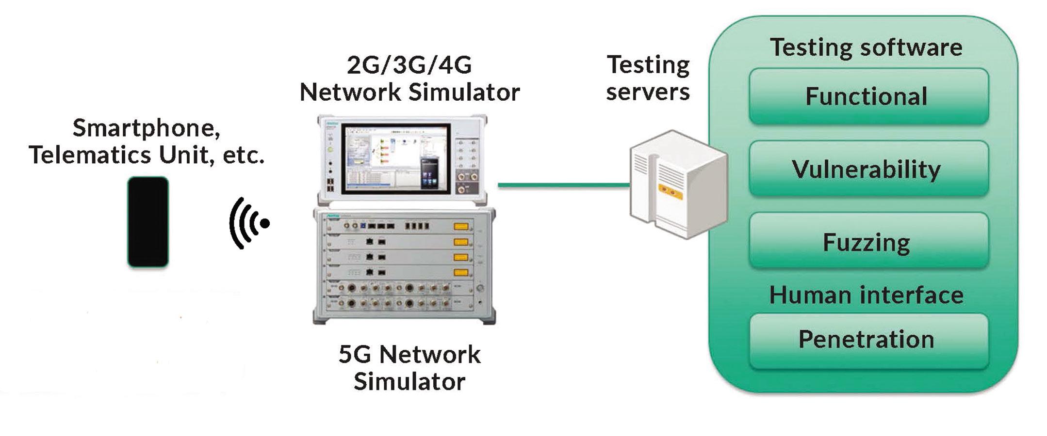
simulator to conduct necessary tests such as functional security measurements. They thoroughly test all security-related functions inside UE or other systems under test to ensure correct behavior and operational robustness (Figure 2). Stress tests and security are primary considerations but hardly the only issues for engineers. Private
in NPN environments. There are new features of 5G NPN that allow the device to selectively connect to the correct network. Verify that a private 5G network is truly only catering to private 5G devices.
· Compatibility: many devices used in a private network
Private 5G networks play a significant role in the fourth industrial revolution. Engineers responsible for developing UE in these use cases must implement test processes that follow 3GPP standards and create real-world scenarios that precisely mirror the specific private 5G network environment. Such an approach will provide greater confidence that the UE will meet established KPIs. •

From the everyday to the extraordinary, you can bring new innovations to market confidently with our proven test and measurement instruments.
We offer everything you need to make ideas real.
Discover more

By understanding the key issues at every phase of the product lifecycle, engineers can make decisions that result in flexible, reliable, and scalable test systems. Taking a modular approach to test system development can accelerate development and mitigate risk throughout the entire product lifecycle.
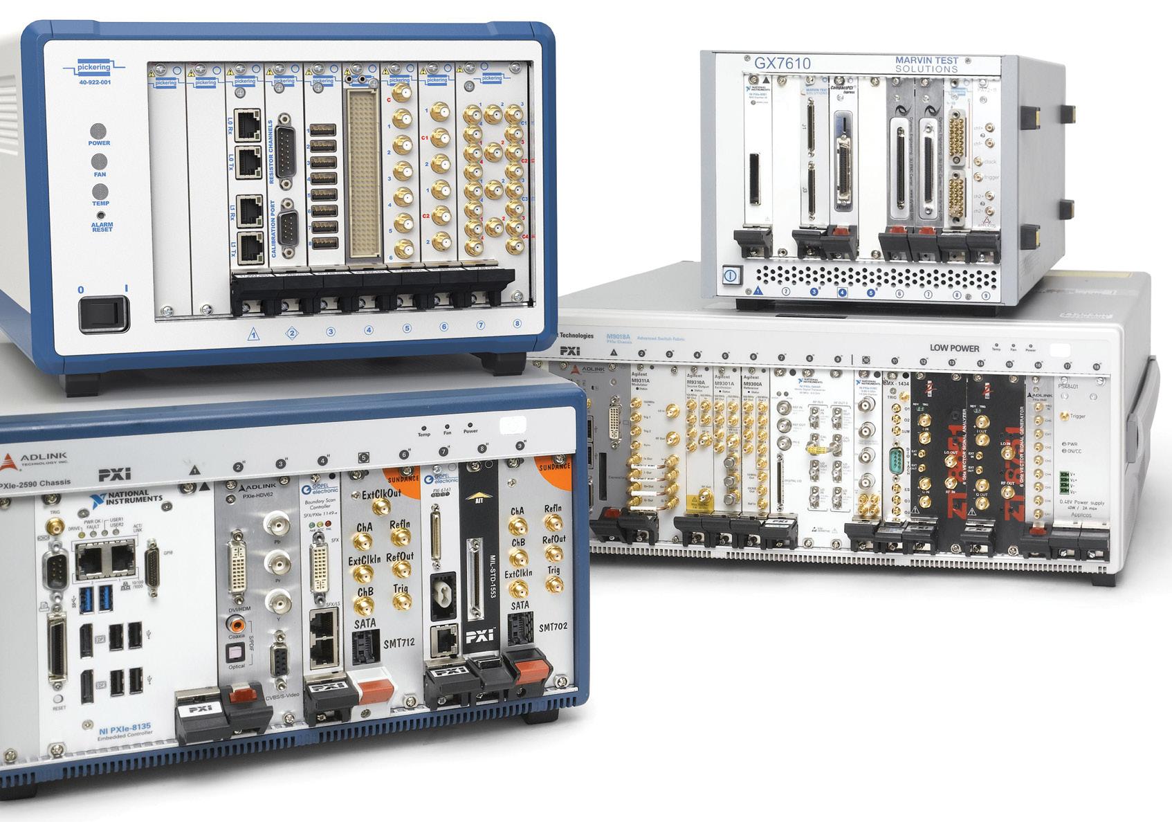
Bob Stasonis, Pickering Interfacesfor Instrumentation bus standard. Introduced in 1997, it is an open, industry-standard, chassis-based architecture that defines how engineers can connect instruments, computers, and other devices using a common bus. PXI systems use the PCI and/or PCI Express buses to interconnect modules in the chassis. PXI offers a wide range of module types from leading global T&M vendors, shown in Figure 1, and can be easily expanded with additional chassis and racks.
When it comes to designing and building automated test systems, today’s engineers find that modularity is key. By using modular hardware, organizations can more effectively manage test equipment from new product introduction (NPI) through to mass/high-volume production. This article will outline some of the key considerations for test-system design in both NPI and production phases, as well as address how modular test systems can evolve throughout the product lifecycle.
Automated test systems have different demands as products they test move through their lifecycles. During NPI, engineers verify design
requirements. As products move to mass production, test systems validate the product. Finally, as products evolve or become obsolete, test systems may need modification, or equipment can be reused for new projects.
Modular test systems typically consist of computer-controlled chassis housing multiple instruments, power supplies, and switching modules interconnected to form complete automated testing stations. Such test systems allow for easy upgrades to support new products, as well as straightforward replacements of defective modules. PXI has become the dominant modular hardware platform for electronic test, measurement, and automation applications.
Why PXI?
PXI is short for the PCI eXtensions
Phase
As products move through their lifecycles, organizations face different challenges. In the early stages of NPI, for example, there is a need to quickly and efficiently test the product to verify design requirements. This can be best accomplished by taking into consideration the following:
Bridging the gap between design and test engineers
One of the best ways to ensure an effective and efficient test system is to think about test requirements early in the design phase. Design engineers will primarily look for their designs to fulfill the product requirements without always thinking about how the product testability in a production environment. By bringing test engineers into discussions early, they can advise on any testability issues
that may need to go into the product design.
Engineers in these discussions should consider all products the system may need to test, ideally including potential future product enhancements and new designs. This will help ensure that the test system design incorporates the necessary flexibility and scalability to efficiently handle such future requirements.
Evaluating test equipment's ease of use and adaptability
Once the product specifications and test expectations are set, it’s important to get the test system up and running quickly. Rapid development and deployment of the test system lets engineers verify the product and move forward as quickly as possible.
Upon first run of a test system, issues may arise. As the debugging process takes place, erroneous connections can damage subsystems, so being able to quickly diagnose and repair
failures is imperative to keep the testing process moving forward. By using flexible test equipment, engineers can rapidly adapt the test system to design changes without having to redesign it.
Cost and availability are always important, but design engineers sometimes only consider the verification testing needed in product development. If the same test system design is needed for high volume production test, it may demand repeat purchasing of costly or scarce components, which can result in cost/time overruns in the future.
Engineers can easily reconfigure and adapt modular test systems to meet changing needs as a product is being defined. Design a new test system as early as possible in the product-design
process. Base it on an industry-standard modular architecture, which helps organizations address the considerations discussed. While modular instruments provide flexibility, some test systems require boxed instruments connected over wired buses such as USB, Ethernet, or GPIB.

Using an industrystandard platform doesn’t tie you to a specific vendor. Instead, engineers can mix and match the bestperforming components from any vendor as needed. Similarly, modular systems don’t tie you to a specific programming interface or operating system, which lets you use their preferred platform and tools, including graphical programming or automated signal routing.
Phase 2: moving from NPI to high-volume testing
When products move from the validation

testing needed for NPI to production test, engineers no longer check for product design faults; they’re looking for component or manufacturing faults. A well-planned NPI test system can evolve and scale to production testing if it is designed with the following in mind:
Considering available resources
Footprint, cost, test accuracy, and availability are all important when moving to a production test system. In the NPI phase, engineers are usually working with a full test bench, providing adequate space for equipment. On the production floor, space is limited. Component cost and availability also have implications on production testers — where an organization may only need one tester for NPI, they’ll often require multiple systems for the production floor. That might mean two to dozens of systems to address production volume.
For high-volume production, you must optimize the productivity of all test processes to minimize the number of test systems required to meet production demands. This entails minimizing the setup and test execution time of each system. The device under test (DUT) must quickly and reliably connect and disconnect from the test equipment so that time is not wasted between units as it moves through
the test system.
Making those connections requires reliable interfacing and possibly even incorporating mass-interconnect systems for products with particularly high changeover rates. In these cases, all connections are made simultaneously through reliable, high-usage connectors in a standard streamlined interface, as shown in Figure 2.
To minimize any adverse impact on production, test systems must be reliable and quick to repair if a fault develops. Also, because production testers are often handed off to test technicians in different locations, and even countries, they need to be easy to operate and well-documented. Similarly, production testers may need to integrate with factory management systems. Industrystandard controllers and programming interfaces will help facilitate these objectives.
PXI offers a rugged mechanical form factor and all the reliability benefits of the PCI and PCIe architectures, including industry adoption and
commercial off-the-shelf (COTS) technology. An industry consortium defines hardware, electrical, software, power, and cooling specifications. As a result, every PXI module benefits from a controlled, stable environment. Modular architecture means that if a module fails, it can be easily tested, swapped, or repaired without affecting the operation of the other modules in the system. Because PXI has a standard form factor, chassis are easy to integrate with standard mass-interconnect systems available from several vendors.
In production test, standard modular platforms typically have an architecture capable of maximizing throughput. For example, PXI instrumentation and switching modules can be integrated into a single chassis with builtin high-speed timing and synchronization, while standard embedded or remote controllers can be easily upgraded to faster models as they become
available. The PXI standard also supports the latest PXI Express (PXIe) format, which provides higher bandwidth for faster data transfers. Using a platform such as PXI also offers the opportunity for parallel testing of more than one DUT, as instrumentation can be readily duplicated in the same chassis, potentially speeding test throughput.
Phase 3: update test systems as products change
As products evolve, support will always be a factor — it’s inevitable that test systems will need to be modified or components will require replacement. The following considerations set production test systems up for long-term success throughout the entire product lifecycle:
Minimizing the opportunity for errors
Every test system should produce the same test
results, so engineers should look for quality and consistency of performance across multiple test systems. Interconnects can easily prove a failure point as DUTs are mechanically connected and disconnected. Other points of error can come from faulty instrumentation, unreliable or mismatched signal paths that impact signal integrity, switching damaged by DUT faults, or operator error. Regular maintenance checks, knowledge of expected component life, and high-quality documentation all help mitigate these risks.
When a test system moves out of NPI and into production, it must be easy to use, debug, and adapt to design changes. Industry-standard test hardware and software (Figure 3) will provide familiarity, scalability, and flexibility, streamlining tester deployment.
Reliable test equipment vendors and system integrators offer consistent, documented products and tools. Engineers can rely on these providers for long-term support of their products, obsolescence management, and timely updates to enhance test systems with the latest system upgrades.
Modular systems offer improved scalability compared to fixed systems, as it is far easier to add or remove modules to/from a modular system to increase or decrease its capacity. This scalability can be particularly important in applications where test requirements may change over time (such as new products added to a manufacturing line).
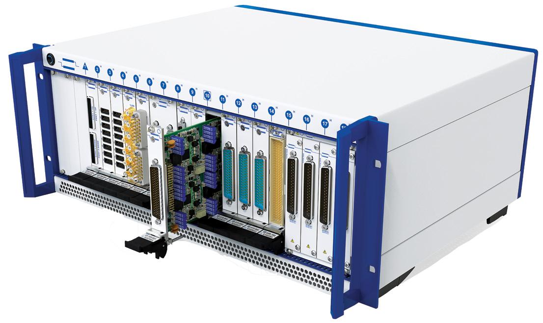
Typically, PXI vendors offer common families of instruments and switching modules, which lets engineers seamlessly scale up within those families to get more I/O connections (Figure 4). Interconnect accessories for modular instruments are also readily available to address
the increased I/O requirements (Figure 3). PXI’s compatibility with mass interconnect systems provides long-term consistent connection capabilities and reduced errors and fault points.
The PXISA, which governs the PXI standard, continues to upgrade its hardware and software specifications, as well as assuring backward compatibility, thereby reducing the risk of obsolescence and protecting the original equipment investment. Whether in the design or production phase, test is critical throughout the product lifecycle. Modular automated test systems, built on industry-standard platforms like PXI, deliver flexibility, reliability, and scalability, helping organizations accelerate development and mitigate risk throughout the entire product lifecycle. •
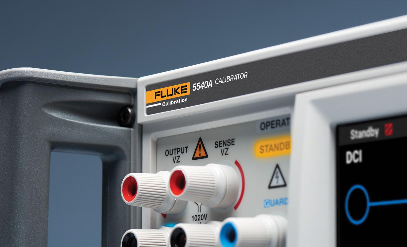
All measurements need reliable, accurate equipment that's traceable to worldwide standards. Without that, measurements have no value.
Michael Johnston, Fluke CalibrationFrom ensuring product quality in a factory to safety to letting every individual use a computer or phone, accurate measurements are critical in every aspect of our lives. In the automotive industry, accurate measurements of components and the tolerances around them ensure that the parts built fit together and that the vehicle is not only drivable but safe. In electronics, accurate measurements of components' electrical characteristics ensure that the product works and meets its specifications. For a device to meet those specifications, it needs measurement. That means measurement equipment. How do you know if the measurement equipment is operating within its required specifications, be those the manufacturer's published specifications or tighter tolerances as needed? That's where calibration and traceability come in.
Every tool used to investigate and troubleshoot your electrical systems needs calibration. The calibration standards used to calibrate them must also be calibrated by equipment that is also calibrated to a much higher accuracy level. Each calibration step in the chain must trace all the way back to the calibration standards. This is metrology, the science of measurement.
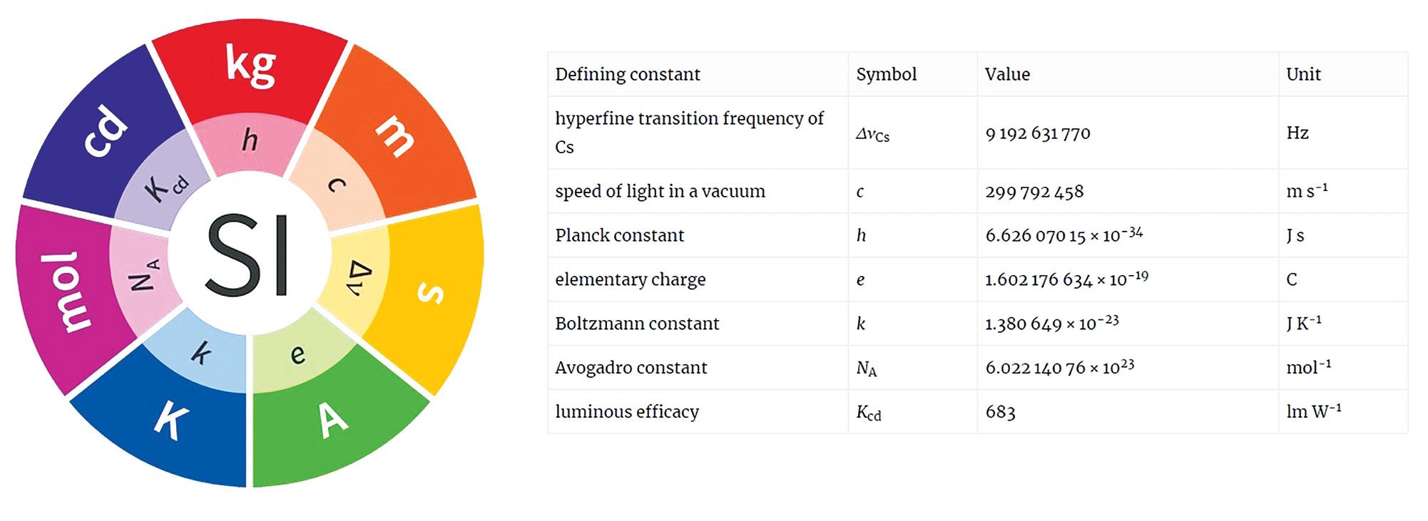
The International Vocabulary of Metrology (VIM) provides a technical definition of calibration and the constants that go with it (Figure 1). To paraphrase: it is a two-step process to first establish a relationship between measurements made with a device
and values provided by measurement standards or references. Each of these calibrations can form a part of how the VIM defines metrological traceability, adding to the measurement uncertainty of the measurement itself.
As you can see, a discussion of calibration and traceability can quickly become very technical, brought on by a string of definitions for us to understand how all the pieces fit together. For this discussion, we can simply think of traceability as a chain of measurements, instrument by instrument, that lead us back to the International System of Units (SI).
Standards are key Metrology has evolved alongside technology. Every advancement in metrology requires and enables more precise measurement capabilities, leading to research, development, and manufacturing improvements. As measurement equipment becomes more accurate, the metrology industry develops better reference devices and methods. Looking back to MIL-STD-120 in 1950, we sought references such as voltage and resistance sources that were five or ten times more accurate than the device under test. By MIL-STD-45662A in 1988, that dropped to four times better.
In 1995 with ANSI/NCSL Z540.1, we began to ensure we were looking at the uncertainty of the whole measurement. That includes all factors affecting a measurement, not just the reference devices. This includes accessories and the calibration uncertainty of the reference devices, which correlate to traceability further up the chain. This further developed in riskbased evaluations with documents such as ANSI/NCSL Z540.3; using the risk of false acceptance of the equipment under
calibration as the driving metric to ensure that our calibrations are adequate.
Each advancement in metrology pushes us forward, requiring a look back at the same time. Any calibrations or new measurement technologies require comparison against SI standards. Until recently, the SI was based in part on physical, artifact-based units that represented some of the base units (the kilogram, kelvin, ampere, and mole).
In 2019, the SI was revised to establish all seven base units of measure on physical constants, all of which are shown in Figure 1. This change was necessary because the original artifacts could erode. These physical artifacts were carefully stored and handled to prevent erosion, but over centuries it’s an inevitability. When it does happen, it can throw off any measurements made from the standard. That was just a level of uncertainty we had to live with. By adjusting the constants, that uncertainty has been removed. By referencing these units to unchanging physical phenomena, uncertainty has been reduced.
Accuracy and uncertainty go hand in hand, though according to the VIM, uncertainty and accuracy are two distinct concepts. Uncertainty is a quantitative figure while accuracy is always considered qualitative. Something can be more accurate or less accurate than something else, but when expressing a value associated with performance, we use uncertainty.
Factors that affect measurement uncertainty, and ultimately accuracy, include the calibration standard used and the associated uncertainty of its own calibrated functions, the measurement instrument's resolution, stability, repeatability, calibration interval, and the measurement environment. Each instrument used in the calibration
chain has a spot in the hierarchy, with the SI sitting at the top. A digital multimeter, for example, is calibrated by a multifunction calibrator. That multifunction calibrator needs calibration by a more accurate multi-product bench calibrator in a calibration lab. In turn, that bench calibrator was calibrated by even more accurate references in one of the National Metrology Institutes (NMI) or other high-level laboratories — Primary Standards Labs — that house their own intrinsic standards that can serve as (realize) SI units themselves.
The references used in these labs can be traced to the SI either as direct representations of the base units or through the calibration process. You can follow as the SI expands from the standards, its physical constants, to calibration instruments that have been compared directly to the standards throughout the industries.
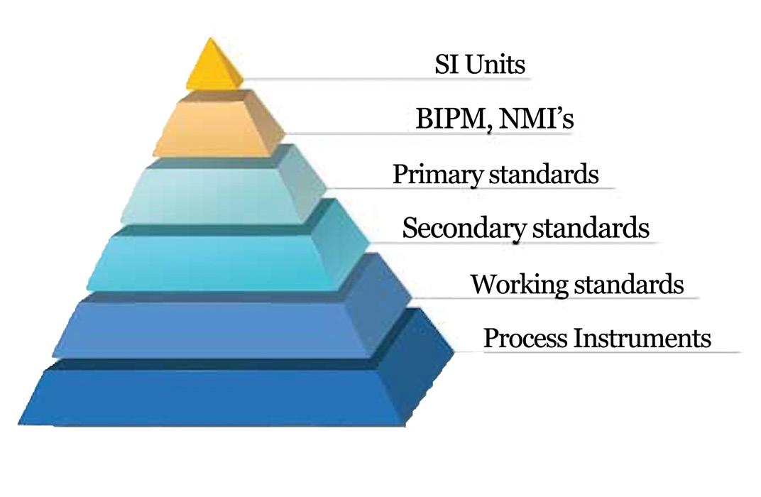
Think of the SI at the top of a pyramid, as shown in Figure 2, where everything below the tip helps pass the SI down to all levels of use. Below the SI sits the BIPM and National Metrology Institutes (NMI), or the groups that facilitate the promotion of the SI within a country.
Every lab or person within a country, however, can’t work directly with the NMIs. NMI-level calibration standards are used to calibrate primary calibration standards or instruments. Those primary calibration standards are then used to calibrate secondary
standards. Those are then used to calibrate working standards. Each of these levels allows for the SI standards to be efficiently and affordably disseminated down the calibration chain.
The need for traceability
Traceability is the process of documenting the calibration chain's hierarchy to the SI. Documenting each step along the way, ensuring that each instrument's accuracy level is within the acceptable uncertainty limit for the equipment and its work demands.
As you head down the calibration chain, or the pyramid in Figure 2, every link or block needs to be connected to the previous one so the calibration performed at any level can be traced up and attached to the SI; this is called traceability. Industries rely on tracking these series of calibrations performed against more and more accurate tools to ensure their measurements are correct. Again, keeping the standards constant around the world and being affordably disseminated.
Calibrations need not be traceable strictly through a National Metrology Institute (NMI) — NIST in the U.S. or NPL in the U.K. — or specifically your own country’s NMI. The ultimate source of truth for all measurements is the SI, and we can follow an unbroken chain of calibrations from the measurements used by industry tools to these seven base units in
a variety of ways.
In the calibration industry, we often hear the misnomer of a “NIST Traceable” calibration. Our true goal is what the VIM defines as metrological traceability to a measurement unit; "metrological traceability where the reference is the definition of a measurement unit through its practical realization."
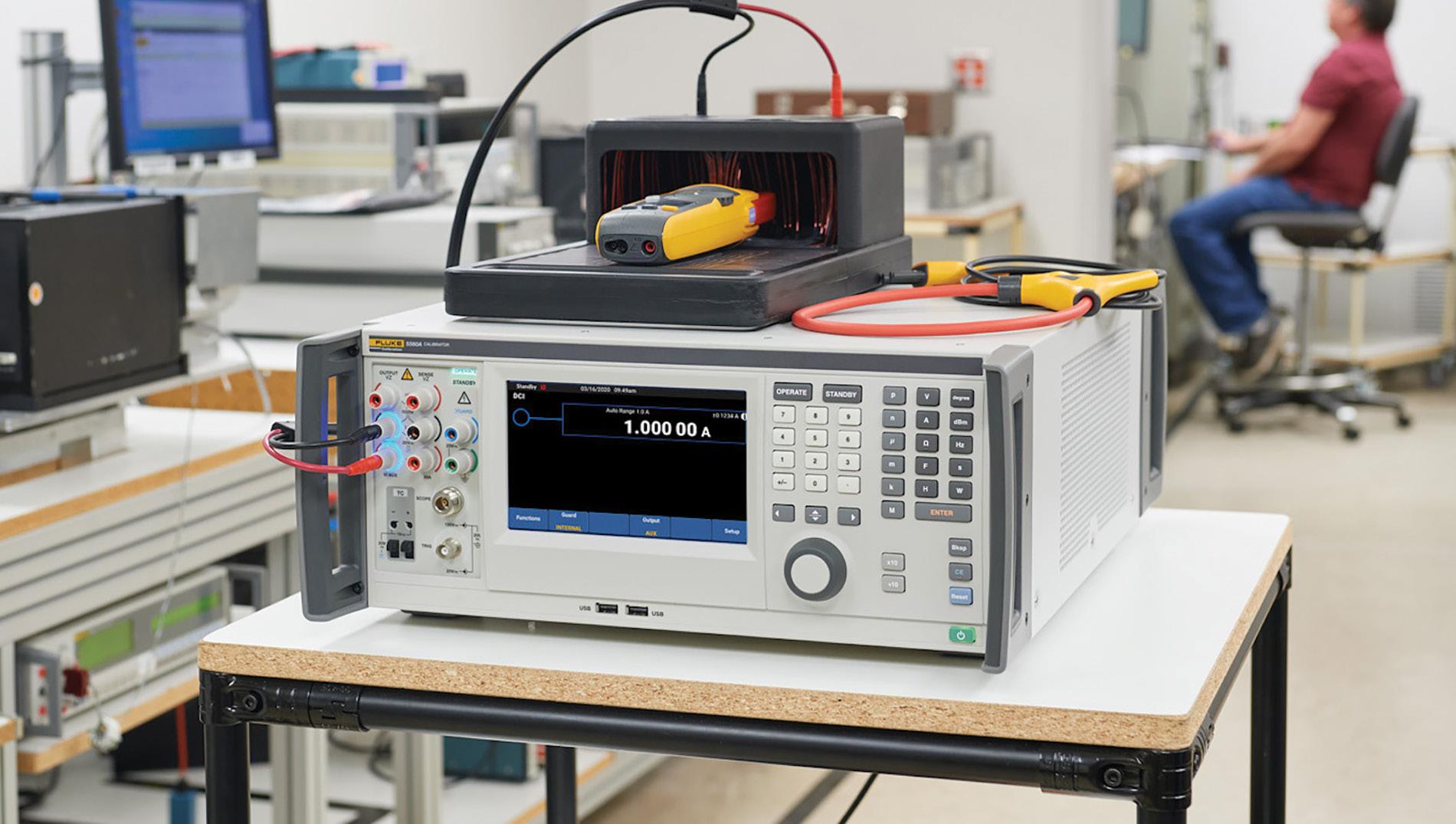
Taking this information one step further, documenting each step in the process, every link in the chain is traceable. Following a series of tools and calibrators right up the chain to the SI helps to show within what uncertainty level each tool’s accuracy sits, meaning you’ll know you can get an accurate measurement to the digit you need. Any more accuracy is wasting money on excessive calibration. Traceability steps form a chain of calibrations from the SI on down to each industry. For an example of the calibration hierarchy and its traceability. In a facility (Figure 3), a clamp meter is calibrated by a multifunction calibrator. That multifunction calibrator was sent to a calibration lab to be calibrated against a more accurate bench calibrator or measurement standard. From there, the next link in the chain is that the measurement standard was calibrated by more accurate references in one of the NMI. Finally, the references used in the NMI have been compared directly against the SI standards to determine the best possible accuracy.
Traceability allows for broad dissemination of the standards while ensuring a tool will measure what it should. Keeping traceability records for every calibration is an important part of the process, not only for metrology as a science, but for the industries using the tools. Many technical and quality
industry standards require proof of the unbroken chain to the pertinent SI units.
Currently, when a tool is calibrated, the calibration work done comes with a certificate as well as records of what measurements were tested and what steps were taken to calibrate. This certificate often includes a statement of traceability, or a list of calibration standards used for the calibration of that specific tool. So far, this process has led each lab to keep its own records. Plus, the actual statement varies from lab to lab, as not all calibration laboratories followed the same industry standards or fit in the same place on the calibration hierarchy. This process involves a lot of paperwork or printing out and storing documents in the hope you can find them if needed later.
With nearly everything becoming digital, so is traceability. Calibration labs are working to digitize calibration certificates. Doing so allows the industry, and each facility, to have a database of traceability for each instrument. The traceability pyramid can become a digital calibration chain, containing information about measurements performed on a tool, as well as what was used above, below, or level with.
The original desire behind creating the SI was one set of measurements "for all times, for all people." Something accessible by everyone, for everyone. Digitizing calibration certificates, in partnership with the refreshed SI constants, brings the world one step closer to that idea. •


Manufacturers of electronic and electromechanical devices rely on test instruments to generate stimuli and measure responses. While manually performing tests on the engineering bench might work for some early prototypes, it's often not given the sheer complexity of today's designs and certainly not feasible for production. That's where automation comes in. Using computers, software, and switching systems lets you automate tests and store test results for analysis.
Because today's products are so complex, you need to logically organize test sequences. You may also need to perform similar tests on several designs. After all, you surely don’t want to write new software each time if possible. You also need an organized process to collect, store, and transmit test data. Therefore, a modular approach to automated test software is essential. At the top of that software chain sits the test executive.
Before explaining what you can do with a test executive, let's start with the hardware that does the actual work.
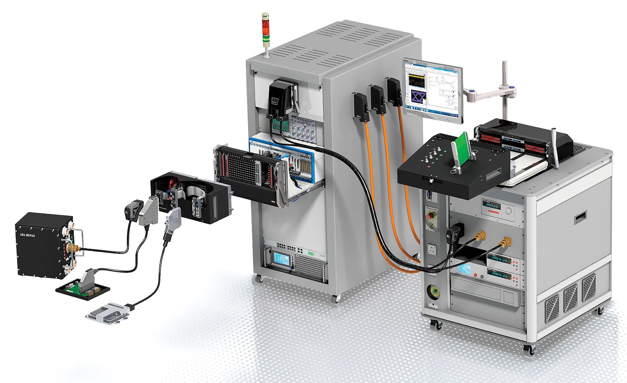
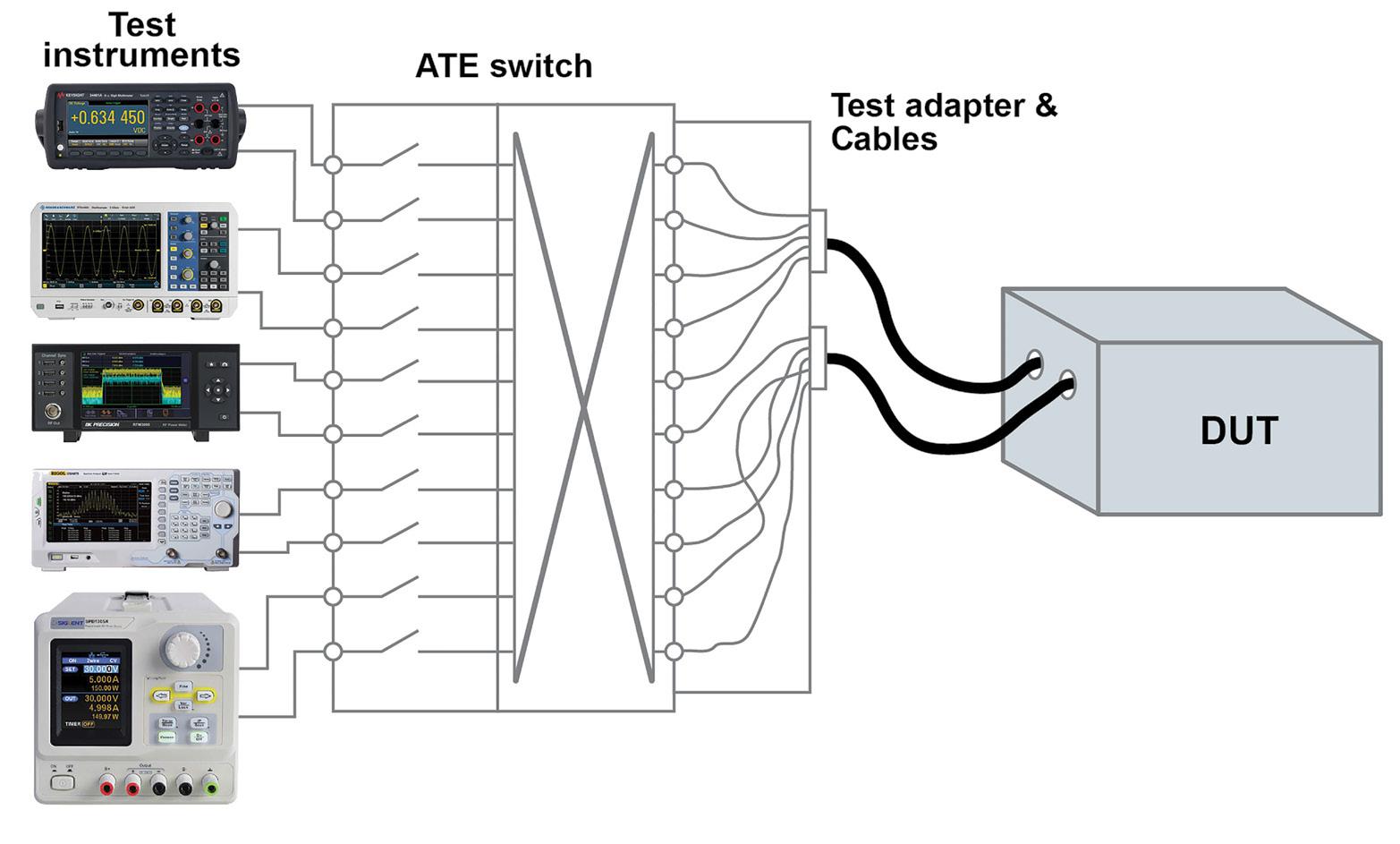
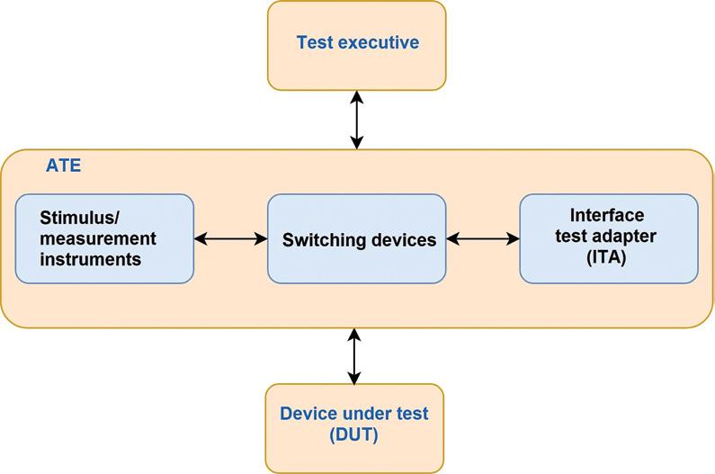
Figure 1 shows a typical (automated test equipment (ATE) hardware setup consisting of test instruments, switches, and a DUT. Many ATE systems include a test fixture and perhaps an interface test adapter (ITA) from the switches to the fixture.
ATE systems need a computer and several software layers that reside between a test operator and the DUT. These layers provide abstractions that shield test operators from the details. They also provide programming interfaces so that engineers developing tests and test sequences don't necessarily need to work
with every instruction that an instrument supports. Instead, engineers can focus on the task of testing.
The details of communicating with an instrument typically fall to an instrument driver. "What is an instrument driver and why do I need one?"[1] explains how instrument drivers create a layer of abstraction between a test engineer writing a test programming set (TPS) and the instrument itself [1]. The TPS tells the driver what it wants the instrument to do. For example, measure an analog voltage without having to deal with the instrument's exact syntax.
What does a TPS do?
A TPS typically contains a sequence of steps needed to perform a specific test, which often involves communication with more than one instrument.
A simple but typical sequence might include:
1. Set a signal source to a specific amplitude and frequency.
2. Set a digitizer to the appropriate range.
3. Set the switches to connect the instruments to the DUT.
4. Collect the test results and take appropriate action.
5. Set the instruments back to a quiescent, stable state and disconnect the DUT from the instruments.
Test engineers program a TPS using a test-programming language (LabVIEW, ATEasy), general-purpose language (C, C++), or scripting language (Python).
What is a test executive?
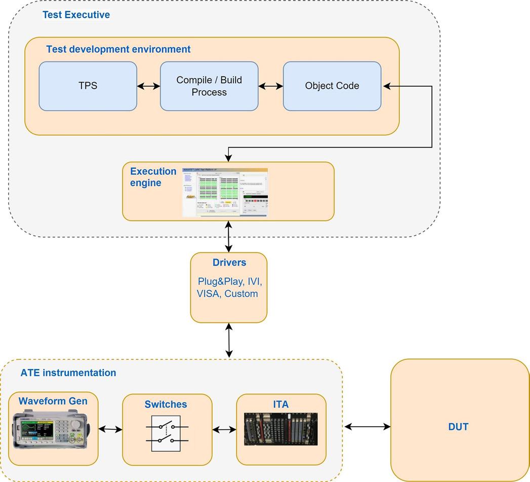
At the top of the software stack sits the test executive (Figure 2), which contains the test operator's user interface and controls the overall test sequence.
A test executive typically contains two main modules:
Working through test-program sets and drivers, test executives let engineers organize tests into logical sequences. They provide user interfaces for test technicians and store test results for analysis.
Bartek Blazejczyk, Astronics Test SystemsFigure 1. An automated test equipment (ATE) station typically includes modular or box instruments and connections to the DUT.
In some applications, these modules are separated and function as two GUIs. In other cases, a single GUI covers both.
Test-development environments come in many flavors. They let test engineers create, develop, and organize TPSs. Some test-development environments require programming knowledge while others let users create test sequences through visual block diagrams.
A test execution engine (Figure 3) executes TPSs by communicating with ATE instrumentation and the DUT (or DUTs) through drivers. A test execution engine takes an input from a built/compiled TPS and executes the test.
A test executive can target multiple UUTs sequentially or in parallel. Semiconductor testing is an example where a test executive stimulates multiple DUTs simultaneously. Depending on the test executive, a GUI could let the operator monitor the test flow status, read the measurement results, and report pass/fail tests. In some
cases, the test executive could store results in a database and present the test outcome as a report. Some environments can interface with automated documentation tools as well as post-processing applications.
Engineers can implement test organization within the test executive differently depending on the platform. The common goal, however, is to create a test flow that includes a series of desired tests starting with setup, which will include all the routines and calls that initialize the test instruments. Once the test executive establishes communication with the instruments, it can move on the executing a test.
Next comes the main test. Typically, it will include all the routines to stimulate the DUT with and measure its responses. Obviously, test looping, branching off based on measurement results, and other conditional execution techniques are available based on the functionality offered a test executive. After all the main tests run, the final module should be responsible for the reset and cleanup. In this stage, all the instruments should be
brought to their quiescent state so there are no longer any active signals present in the station. All switches should be open, thus breaking the paths between the ATE and the DUT. Other functions in this stage can finalize the data recording and make the proper input for reports and data analyses.
How does the test executive communicate?
Engineers can apply different approaches on how to handle communication between the modules of the test system. In cases where there is a separation between the testdevelopment environment and the execution engine, you would need to compile/ build the project first before invoking the execution engine and commencing the test. The main input into the compile/build process is the TPS source code. Once the source gets built into the binary code, the execution engine will take over and start the execution. The code must also have the information that the TPS requests such as data for signals and routines requested in the TPS. That data lets the execution engine call the appropriate instrument driver. In cases where there is no separation between the test development environment and the execution engine, all the compilation and building processes are not visible to the user and they occur in real time when the test commences.
After the engine properly allocates a TPS signal to an
ATE instrument, it makes a call to the driver. As a result, the ATE instrument gets instructed to perform a task described in a TPS. An example of such a task could be applying an AC signal. The driver that the engine selects will call the allocated instrument, in this case, a function generator producing a signal with a specified amplitude, shape, and frequency. The ATE connects to the DUT through the switching instruments and ITA. To route the voltage signal from the function generator to a particular DUT test pin, specific relays in the switching device will close, establishing the path between the ATE instrument and the DUT.
Instrument drivers used in today's test stations typically support interchangeable virtual instrument (IVI) drivers, or some other plug-and-play type that relies on Virtual Instrument Software Architecture (VISA). Test executives routinely support bus interfaces such as GPIB, PXI, VXI, serial (RS232/ RS485), Ethernet/LXI, and USB.
You can write your own test executive but it's a large undertaking. At Astronics, we use commercial test executives as well as those we develop in-house, depending on customer specifications. For example, we use two platforms
developed in-house: PAWS Developer’s Studio, which uses Abbreviated Test Language for All Systems (ATLAS) as a TPS language, and ActivATE test software, which uses C# or VBScript to develop test sequences. The standard options available on the market provide a robust and complete package that typically took decades of development effort to bring them to their current form. The objective of the universal and well-designed test executive is to improve the productivity of test engineers and developers through modern graphical interfaces, different programming languages, reuse, and a host of other techniques. Test executives enable customization, backward compatibility, and legacy protection, which reduces the project lifecycle costs.
Test executives reduce the risk of ATE and software obsolescence. During a test system's lifecycle, which can exceed 20 years, there will be a need to re-host the test station to the current operating system (OS). New test instruments often require an


updated instrument driver. The modular architecture and ability to decouple the TPSs from hardware and driver dependency can make the re-host and upgrade process more manageable, seamless, and cost-effective.
Typically, each TPS undergoes a validation process before formal release. The need to adjust and re-validate the TPS because of the ATE upgrade or OS re-host is time-consuming, costly, and should be avoided or minimized. Some test executives do better in this area than others. These objectives are not easily achievable when developing your own test executive unless you have many experienced developers available. Creating your own test executive will be more of a dedicated solution, which will most likely fulfill the simple test requirements for a given scenario but will lack flexibility and support for long lifecycles. Well-architected test executives can easily interface with third-party tools such as test-require-
ment editors, test-program generators, and automated documentation tools, which might be an additional argument against developing your own.
Commercial test executives have a universal approach, which lets you design test stations that target various DUTs. Creating your own Test Executive solution is certainly a challenging and time-consuming task. •


[1] Rick Nelson, "What is an instrument driver and why do I need one?"
Test and Measurement Tips, Feb. 16, 2023. https://www.testandmeasurementtips.com/what-is-an-instrumentdriver-and-why-do-i-need-one/

The constant need for more throughput in data centers pushes engineers to develop ever-faster optical and electrical links. In addition to designing for more speed, engineers must optimize these links for physical space, power consumption, cost, reliability, and scalability.
Most of the data-center traffic moves into and out of the data centers (north-south traffic). A shift is, however, happening toward distributed computing, which increases server-to-server traffic (eastwest traffic). As east-west traffic exponentially increases, unprecedented levels of data center traffic threaten to outpace the development of new switches. Co-packaged optics can help mitigate signal integrity and power consumption problems, both of
which introduce new test issues.
At the heart of a switch lies a specialized applicationspecific integrated circuit (ASIC) capable of terabits-persecond throughput. Previously, most of these ASICs were developed in-house by the switch manufacturers. That paradigm has, however, shifted with the rise of merchant silicon — ASICs developed by third-party silicon vendors and sold to switch manufacturers for final-product integration.
In traditional switches, the switching ASIC drives the data over multiple channels across the printed-circuit board (PCB) to ports on the switch chassis' front panel. The ports and their pluggable modules have evolved alongside the switching silicon in the form of increasing speed or number of channels per link.
As Figure 1 shows, the throughput per port has grown exponentially from the original small form factor (SFP) 1 Gb/sec links to the
latest Quad-SFP double-density form factor (QSFP-DD 800) supporting up to 800 Gb/ sec. Modules with copper cabling, otherwise known as direct-attach copper (DAC), can connect switches to one another. Unfortunately, copper cannot handle the speeds and distance necessary for most data-center communication. Instead, data centers leverage fiber-based optical interconnects between switches to preserve signal integrity over long distances with the added benefit of lower power consumption and better noise immunity. Fiber cabling requires transceiver modules in the switch ports to convert signals from the electrical domain of the switching silicon to the optical domain of the cabling and back. Figure 2 shows a conventional transceiver with
two key components: the transmit optical subassembly (TOSA) manages the electricalto-optical conversion while the receive optical subassembly (ROSA) manages conversion in the opposite direction. The copper fingers of the transceiver plug into the switch while an optical connector plugs into the other end. The optical connectors come in an entirely separate variety of form factors and variants. Multisource agreement groups (MSAs) work to ensure standardization and interoperability between vendors as new transceivers and cable technologies enter the market.
The path between the pluggable transceiver and the ASIC consists of copper-based serializing and deserializing
Integrating optics into the same package as switching ASICs improves signal integrity and increases data rates, but challenges remain. Near-packaged optics could emerge as an interim solution to the problem.
(SerDes) circuitry. As the switching silicon scales, the copper interconnects must equally scale, which switch vendors achieve by increasing either the number or speed of SerDes channels. The highest-bandwidth switch silicon today supports 51.2 Tb/sec, which manufacturers accomplished by doubling the number of 100 Gb/sec PAM4modulated SerDes lines from 256 to 512.
If a 51.2 Tb/sec ASIC serves a front panel of 16 ports, the switch requires a 3.2T link at each port to fully utilize the provided switching capacity. While today’s highestbandwidth pluggable implementations provide 800 Gb/sec per port, standards groups are actively working to expand the capacity of these links through channel density and speed (e.g., 16 channels at 200 Gb/s to reach 3.2T). Table 1 shows the progression of symbol rate, data rate, channels, and aggregate capacity over the years.
Research is underway into 224 Gb/ sec technology, which yields a 200 Gb/sec SerDes data rate and would enable the use of 1.6 Tb/sec interfaces at the front panel. With increased speed, however, comes the added challenge of more complex signal transmission methods and higher power consumption per bit. Evolutions moving toward 224 Gb/sec have helped to avoid the ominous predictions made in the early 2010s that forecasted skyrocketing power consumption scaling with traffic through data centers. Figure 3 shows how competing factors have kept data center power consumption relatively steady.
Along with updates to network layouts and cooling systems, the increased data rate for a single switch allowed for a smaller number of devices, thus reducing the footprint and overall power consumption. Technology experts suggest that we are approaching a physical limit of copper channel data rates within the existing server form factor. While breakthroughs in interconnect technology have supported scaling to 800 Gb/sec links and 1.6T, driving beyond these data rates will require a fundamental change in switch designs.
As the SerDes speed and density continue to increase, so does the power required to drive the signal and preserve the signal across PCBs. A large component of the power increase comes from the additional
re-timers used to ensure proper data recovery at the receiver. To reduce the power that the switch needs, research groups and standards bodies have been pursuing methods to shorten the copper distance over which the signal must travel.
The Consortium for On-Board Optics (COBO) represents the earliest collaboration to move the signal conversion away from the front panel closer to the ASIC. On-board optics (OBO) move the primary functionality of the pluggable transceiver to a module on the switch’s PCB, shortening the copper channel where electrical signals cross. This methodology relies on recent advancements in silicon photonics, where optical functions are built into the die fabrication process. Silicon photonics enable more compact conversion options in the form of optical engines (OEs), which have lower costs and use less power than conventional pluggable transceivers. While these improvements help to reduce the copper channel length, the improvements have not yet outweighed
the complications introduced in deviating from the industry-standard pluggable architecture. Based on this, the industry may leapfrog OBO to a more advanced form of integration.
Beyond OBO, the terminology becomes debatable. The term nearpackage optics (NPO) describes optical engines placed on the PCB or interposer along the boundary of the switching silicon’s substrate. This method reduces the electrical channel path even further than OBO but still requires significant power to reliably drive the SerDes signals. Near-package optics could prove to be a great transitionary step as it provides significant signal benefits and reuse of the existing silicon designs — at the small price of requiring a new approach to relaying optical signals from the front panel to the optical engine.
Co-packaged optics (CPO) is a design approach that integrates the optical engine and switching silicon onto the same substrate without requiring the signals to
traverse the PCB. The levels of integration between the optical and electrical functions of the package exist on a spectrum, some of which appear in Figure 4.
For instance, some devices leverage a 2.5D co-packaging strategy, which places the optical engines on the same substrate as the ASIC with millimeter-scale connections between the two. Some manufacturers use a 2.5D chiplet integration system to provide flexible interface options to the silicon (e.g., mixed-use of co-packaged optics and pluggable transceivers), demonstrated in Broadcom’s Tomahawk 5 co-packaged optics switch.
Even more integrated co-packaged optic designs are in their nascence, including:
· Direct-drive configurations where the digital signal processing migrates from the optical engine to the ASIC
· 3D (stacked) integration between the optical and electrical functions
· Integration of the driving lasers into the package
· Fully integrated monolithic electro-photonic ICs
Impact on test
While technologies such as CPO and NPO reduce the span over which electrical signals must travel, providing both signal integrity and power consumption benefits, the interoperability requirement remains. That is, the optical data signal from the transmitter must traverse an optical channel and be correctly received at the other end by a receiver that may have been produced by another vendor. The signals will likely need to comply with specifications such as those developed in IEEE 802.3.
A key difference compared to testing pluggable optics is in the difficulty and expense to correct a problem once the CPO/ NPO has been integrated into the switch. The CPO/NPO cannot be easily swapped out like a pluggable module. Test strategies must evolve to not only verify signal performance for compliance
but also identify problems early in the manufacturing process, with additional testing to ensure long-term reliability. While the electrical path to the CPO/NPO may be over shorter distances, the high symbol rates will require careful design, validated with the same test and measurement methods employed for classic chip-tomodule interfaces.
While there are many paths to co-packaged optics, challenges around these new technologies work against rapid adoption. Adopting new technologies overnight and the progression toward new standards requires a path for data centers to gradually upgrade or replace their infrastructure while also getting component manufacturers to incorporate new technology by iterating on existing designs.
Key challenges manufacturers and data centers face include:
· Development and standardization of new fiber-based front panel connections
· Silicon flexibility that allows for the co-existence of pluggable, onboard, near-packaged, and/or co-packaged optics
· Service and replacement of components
· Manufacture and yield of advanced packages
· Return-on-investment for data investment remains unproven
While these hurdles may ultimately outweigh the benefits achieved by co-packaged optics, it is difficult to deny the possibilities created by moving in this direction. Whether or not copackaged optics see widespread adoption, the explosive forecast in data traffic signals an approaching and necessary end to how we do things today, ushering in a new approach to data center interconnect technology. •

Theneed to reduce carbon emissions drives investments in electrical technologies, particularly in data centers and electric vehicles. In its most recent Elective Vehicle Outlook report, Bloomberg estimates a 27% increase in global electricity demand caused mostly by electrifying nearly all of road transport by 2050 [1].
Wide bandgap (WBG) semiconductors, including gallium nitride (GaN) and silicon carbide (SiC), are replacing silicon-based power MOSFETs and IGBTs in switch-mode power supplies and motor drives. GaN and SiC devices have faster switching speeds, higher power density, higher frequency response, lower leakage, lower ON resistance, and higher operating temperatures than silicon. These characteristics result in greater operating efficiency. They can reduce energy use, making it easier to comply with regulatory and certification requirements as well as current JEDEC JC-70 wide bandgap power electronic conversion semiconductor standards. Compliance requires testing.
WBG brings new test methods to the table. As engineers continue to study WBG technologies, they learn more about the behaviors of these devices and their performance. The common transistor architecture for SiC and GaN is the MOSFET and HEMT, respectively. Both offer advantages over the other, but both come with their own set of measurement challenges.
While the tests required during design and production are like those of silicon-based devices, the adoption of WBG materials requires added rigor for
higher voltage and current levels to accurately measure performance and long-term reliability. High-power devices such as SiC MOSFETs operate at voltages well over 1000 V, even as high as 5000 V. With current levels in the tens to hundreds of amps, it’s becoming more common for engineers to talk about kilowatt to megawatt power levels. These levels require new testing strategies and — more importantly — an emphasis on safety.
To fully validate SiC or GaN-based WBG devices, engineers must test several parameters using a test setup such as that shown in Figure 1. Parameters include:
∙ Switching loss: precise time alignment is critical. Nanosecond errors in capturing signals can result in incorrect results.
∙ Peak voltage: voltage spikes commonly occur during high-current, high-speed hard switching.
∙ Peak current: fast switching operation of WBG transistors causes sharp current spikes that stress devices and may reduce lifespan.
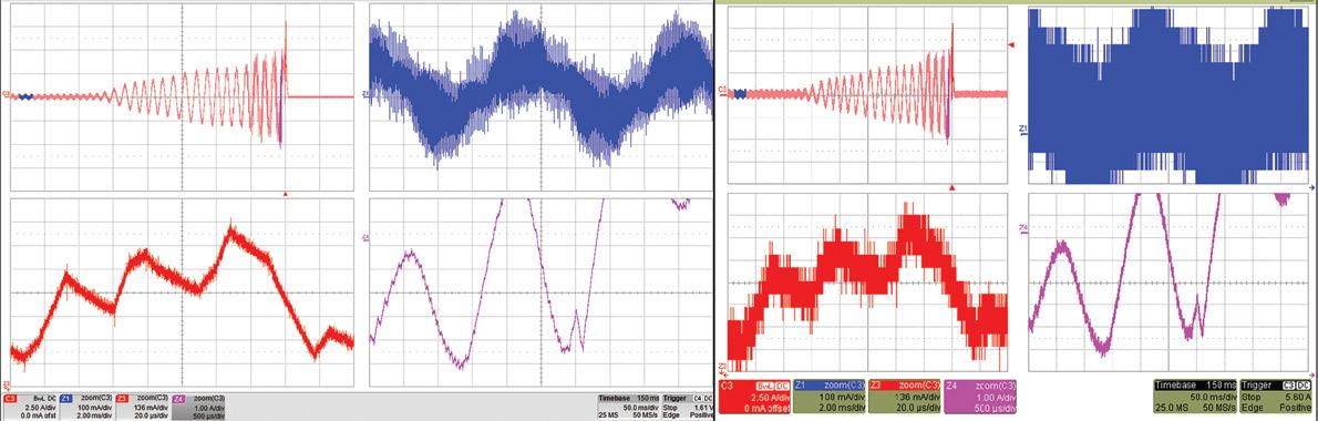
∙ Reverse-recovery charge: this behavior must be quantified to understand its contribution to total losses. Figure 2 shows reverse-recovery charge waveforms.
The preferred test method to measure the switching and diode reverse-recovery parameters of WBG devices is the double-pulse test (DPT). DPT can be an efficient process for making several critical measurements to help validate and optimize these power converter designs. Figure 3 shows a typical test circuit.
Performing DPT lets you:
By automating double-pulse testing of wide bandgap devices such as SiC and GaN power devices, you can cut setup and analysis time.
Jonathan Tucker, TektronixFigure 1. Double Pulse Test Setup uses oscilloscopes, a multimeter, and a source-measure unit. Figure 2. The reverse-recovery waveforms in the top part of the display show an overlapped plot of multiple events.
∙ Guarantee specifications of power devices like MOSFETs and IGBTs.
∙ Confirm the actual value or deviation of the power devices or power modules.
∙ Measure switching parameters under various load conditions and validate performance across many devices.
To define a DPT signal, you need two pulses of different widths (Figure 4). The first, longer pulse establishes current in the inductor (shown in Figure 3) that replicates circuit conditions in a converter design. You'll need to adjust the pulse width to get to the desired test current.
The second pulse is shorter than the first pulse to prevent the device from overheating but long enough to make the measurements.
You can use manual methods to create pulses with varying pulse widths, which can be time-consuming. Some of these methods include creating waveforms on a PC and uploading them to a function generator. Others use microcontrollers that can require more time to program.
As materials researchers and device engineers explore new and more advanced devices, such as those that could be based on Gallium Oxide, Aluminum Nitride, and even Diamond, new approaches to DPT methodology may arise.
Instead of the arbitrary function generator (AFG) outputting a programmed double pulse sequence, it can be programmed to output a series of equally-sized pulses. Cumulatively, these pulses can deliver the same current as the initial pulse in a normal DPT. Such an approach has been suggested in this peer-reviewed journal paper [3]. The good news is that the instrumentation and the software that runs the test can be modified for new approaches.
Engineers interested in understanding the switching, timing, and reverse-recovery behaviors of WBG power devices can use automated DPT methods to shorten test time. Oscilloscopes with measurement software can automate test setup, execution, and analysis.
Figure 5 shows a typical setup screen. Adjust the first pulse width to get the desired switching current values. Then, adjust the second pulse to avoid destroying the power device. You can also set time gaps between the pulses.
Careful probing and optimization will help you get good results. You can take steps to make accurate and repeatable measurements. For example, removing voltage, current, and timing errors from the measurement. Automated measurement software eliminates manual steps, saving time and providing repeatable results.
Conclusion
DPT is the preferred test method to measure the switching
achieve worldwide progress on carbon reduction can only go so far. By researching and testing new materials, we can get closer to the goal of meeting energy demands and adopting new efficiency standards. There's still time to reduce Bloomberg's estimated 27% increase.
[1] Electric Vehicle Outlook 2022, BloombergNEF, https:// about.bnef.com/electric-vehicleoutlook.
[2] JC-70 Wide Bandgap Power Electronic Conversion Semiconductors, JEDEC, https:// www.jedec.org/committees/ jc-70.
[3] Mohammad H. Hedayati, Harry C. P. Dymond, Rajib Goswami, and Bernard
parameters and evaluate the dynamic behaviors of power devices. Automated DPT setup and analysis can greatly reduce test times and achieve faster time to market for nextgeneration power converters. Tests can easily run with full remote control, letting you keep your distance from the highvoltage, high-current DUT for added safety.
Without the ability to measure critical values and ensure functionality, your ability to meet energy demands and
H. Stark, "Investigating GaN power device double-pulse testing efficacy in the face of VTH-shift, dynamic Rdson, and temperature variations," 2021 IEEE Applied Power Electronics Conference and Exposition (APEC), https://ieeexplore.ieee. org/document/9487358.

Power integrity is a subset of signal integrity, whose assessment ensures that signals have suitable amplitude, rise time, noise, transient, and other characteristics for proper circuit performance under all operating conditions. Power integrity focuses on these same characteristics for the power distribution network (PDN) power rails to ensure that devices receive supply voltages that fall within the device’s specified operating ranges under all circuit operating conditions. Measurements play a significant role in power integrity.
Supply voltages in the PDN must be kept within a specified tolerance of their nominal value. A PDN's noise, droop, and transients also need tight control. Cumulatively, this might mean an allowable power-rail variation of less than 1%, depending on the circuit. Therefore, a 1 V power rail might need to have variations in the rail voltage limited to ±10 mV (or
less). Moreover, bandwidth of the noise and transient signals on the power rail can extend beyond 1 GHz. Measuring the small (millivolt) variations of the power rail at relatively high bandwidths can prove challenging.
Figure 1 shows a typical embedded system. Its PDN includes voltage regulator modules (VRMs), low dropout (LDO) regulators, board interconnects, PCB power and ground planes, and bulk decoupling capacitors. Packaged semiconductor devices have internal power rails not shown in Figure 1 and are the focus of additional on-die power integrity analysis.
Noise and transients encountered in power-integrity
measurements arise from many sources. Self-aggressive noise can arise from VRM to VRM, or the noise could originate at a processor core, I/O signals, or the VRMs. Mutual crosstalk between any of the circuit elements may also contribute.
When making power-integrity measurements, your goal is to assure the voltage levels of the rails (regulation) and to characterize the noise on the rails (e.g., ripple, droop under transient load conditions, pollution from other sources, etc.). Figure 2 shows an example of typical power-integrity measurements.
This analysis of a 1.5 V rail uses automated measurements to find the mean rail voltage and the peak-to-peak noise amplitude. A Fast Fourier Transform (FFT) lets you view the rail's frequency spectrum. The frequency-domain view is a useful tool for analysis and troubleshooting. Most oscilloscope manufacturers create a dedicated spectrum analyzer user interface within the oscilloscope.
The key oscilloscope specifications relevant to power-integrity measurements are amplitude resolution, bandwidth, sample rate, vertical offset range, and memory length.
Amplitude resolution specifies the smallest amplitude difference in the
Ken Johnson, Teledyne LeCroy
is crucial when evaluating circuit power quality because it has a direct influence on performance.
acquired waveform that the oscilloscope can resolve. It is usually specified in terms of the number of bits of the oscilloscope’s digitizer. Assume you're measuring 5 mV of ripple or noise riding on a 1 V rail. The ripple voltage is 46 dB (200:1) lower than the rail amplitude. A rule of thumb is that an oscilloscope’s theoretical amplitude dynamic range is 6 dB per bit. An 8-bit oscilloscope may have a usable dynamic range of 48 dB (at best), while a finer-resolution oscilloscope oscilloscope will have a wider dynamic range. This difference appears in the comparative signal clarity of the two captures in Figure 3.
An oscilloscope's bandwidth limits the range of frequencies that the instrument can measure. While the rail signals are nominally at DC, rail noise and transients can have a wide frequency range. In general, PDN powerintegrity measurements require oscilloscope bandwidth from 500 MHz to 2 GHz to accurately capture noise and transient events on the board-level power rail, with even more bandwidth required to measure closer to or on the die rails.
An oscilloscope's maximum sample rate must be greater than twice its bandwidth. Most modern instruments have minimum oversampling of four or five times the bandwidth, and this increases the horizontal (timing) resolution and the ability to accurately capture high-speed transients. The sample rate also sets the upper-
frequency limit of the FFT at half the sampling rate.
The vertical offset range sets the maximum vertical sensitivity you can use to measure a power rail, depending on the probe you use. The oscilloscope's offset shifts the DC rail voltage and centers the power rail signal vertically on the oscilloscope grid. Adjusting the oscilloscope's gain sensitivity to 10 mV/div or less lets you view small amplitude changes on the power rail. A typical oscilloscope may have 1 V of offset (or less) at the highest sensitivities (e.g., below 100 mV/div or 50 mV/ div) — not enough to center the power rail and view transients at the highest sensitivities. Oscilloscopes optimized for power-integrity measurements provide enough offset at higher sensitivities to not limit rail measurements. Furthermore, attenuating probes, such as the 10:1 passive probe supplied with your oscilloscope, restrict the instrument's offset range because the probe's attenuation factor shifts the oscilloscopeplus-probe combination offset range by the attenuation factor. An oscilloscope with an offset specification of 1 V at 5 mV/div will, for example, be restricted to
1 V of offset at 50 mV/div (10 times 5 mV/div) when using a 10:1 passive probe. This restricts the highest sensitivity gain setting that you could use to view small voltage ranges. Using a home-built coaxial rail probe or a specialized power rail probe can minimize the impact of the offset range either by reducing the attenuation or increasing the offset range.
The oscilloscope’s acquisition memory length sets the record's maximum duration, which is important for operations such as measuring power sequencing at startup and shutdown. Large amounts of acquisition memory can help you understand and debug complex cause-effect scenarios in an operational system when looking at many power rails at once. The maximum acquisition length also determines the FFT's frequency resolution.
Viewing power rails requires a probe. There are several considerations in the choice of an oscilloscope probe for power-integrity measurements. The first is that the signals of interest are often small voltages atop larger DC voltages, and the noise that the measurement system (oscilloscope plus probe) contributes must be smaller than the signals of interest. The oscilloscope-probe combination must have sufficient bandwidth to not alter signal components of interest. The PDN’s power rail may carry only a small amount of current, and the probe should not load the power rail (draw too much current in comparison to what it is designed to carry).
Impedance differences between the probe and the PDN will also cause reflections of highfrequency components. Finally, the instrument system should have sufficient offset to match the rail voltage when the probe is connected.
The first probing option is the use of the 10:1 passive probe usually supplied with the oscilloscope. This passive probe uses a 9 MΩ resistor in series with the oscilloscope’s 1 MΩ input, forming a 10:1
attenuator. This attenuator is compensated by using a small capacitor in parallel with the 9 MΩ resistor, forming a highpass filter that compensates for the low-pass characteristic of the oscilloscope’s input. An adjustable capacitor in the probe compensates the attenuator by making the highpass and low-pass filter cutoff frequencies equal. Always compensate this type of probe whenever you connect it to an input channel.
An oscilloscope's 10:1 passive probe has some limitations. The 10:1 attenuator reduces the input signal supplied to the oscilloscope input, which the oscilloscope must then scale back up. Therefore, the additive noise of the probe is ten times, or 20 dB, greater than the actual noise.
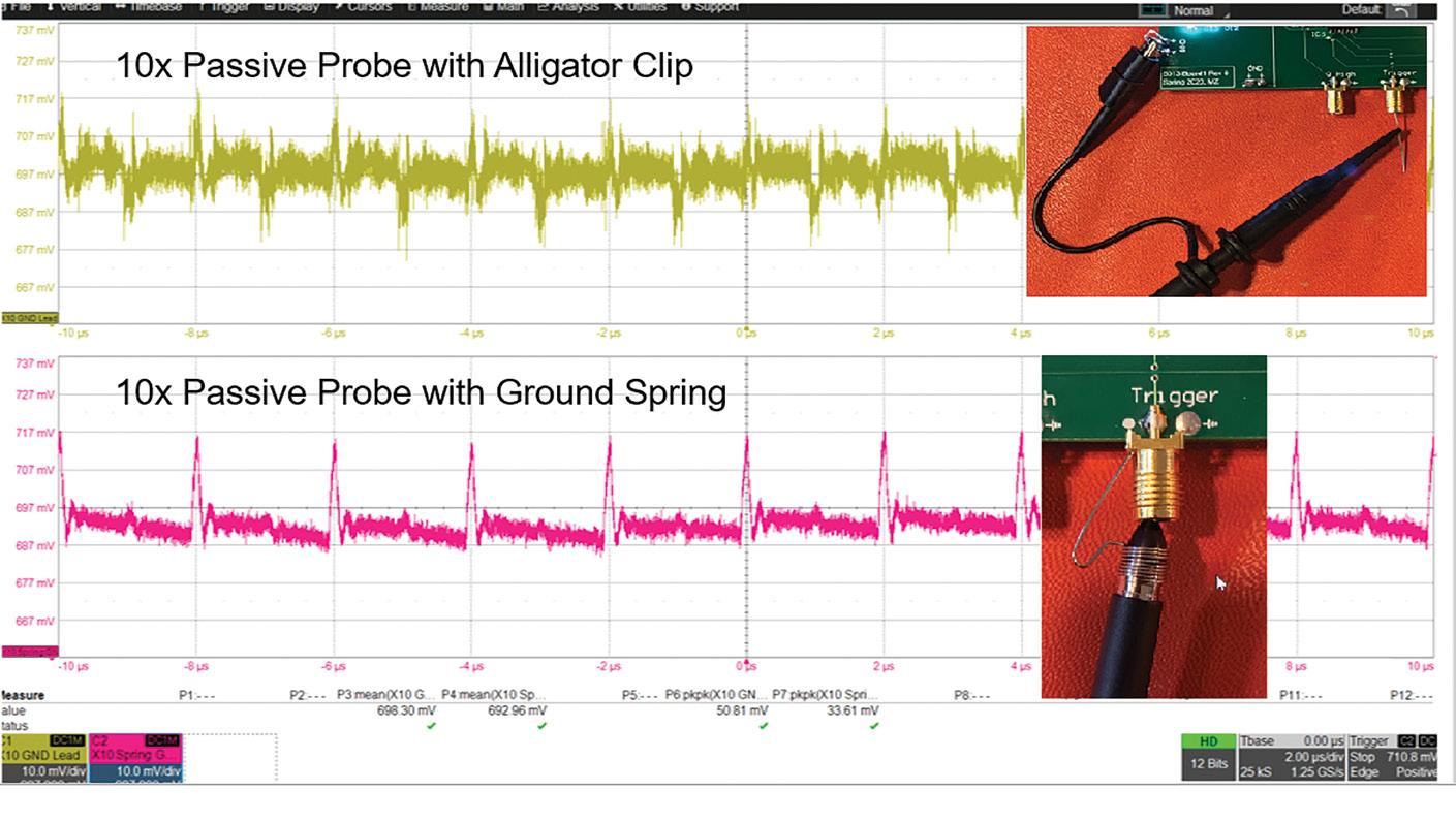
The 10:1 passive probe often comes with a variety of tip accessories for different interconnection methods, the choice of which can affect its performance. The most often used accessory is the spring hook, which uses a long ground wire terminated with an alligator clip. This combination
works well for low-frequency signals — higher frequency measurements will incur noise because the probe's ground wire forms an antenna through the ground loop. Instead, use a ground spring accessory, which employs a spring wrapped around the probe’s ground ring with a very short projection. This minimizes the high-frequency pickup. Figure 4 shows the variation in noise pickup for each method.
A coaxial connector adaptor accessory may also come with the passive probe, or you can purchase it from third-party suppliers. It can mount on the board, which reduces noise pickup.
You can also use 10:1 transmissionline probes that terminate into the oscilloscope's 50 Ω input. These probes offer short leads and wide bandwidth (greater than 1 GHz). Like the 1 MΩ coupled 10:1
passive probe, the transmission line probe attenuates the input and increases internal noise scaled to the connection point. External noise pickup is low, but this type of probe has a lower input impedance of 500 Ω, which may cause loading problems.
You can also connect a 50 Ω coaxial cable directly to the power rail to use as a probe. There is no attenuation with this connection, so there is no additive noise. If the coaxial cable is terminated into the 50 Ω input of the oscilloscope, then the cable input is a 50 Ω load on the connection point. This can cause circuit loading problems, especially if the power rail supplies very small currents. For example, for a 5 V rail, the oscilloscope input would draw 100 mA, and this could be a considerable load current for a battery-powered device. Most oscilloscopes also limit the maximum voltage at the 50 Ω input to 5 V or less — make sure you don’t exceed this input limit or you could damage the oscilloscope's input amplifier.
Using a coaxial cable terminated into the oscilloscope’s 1 MΩ input may
work for low-bandwidth (below 500 MHz) measurements, but this arrangement will result in high-frequency reflections. If you can recognize the signature of these reflections (and ignore them in your circuit assessment), this may be a good, low-cost technique that minimizes loading and reduces additive broadband noise.
The final probing method is a power-rail probe. The power rail probe, as the name implies, is designed specifically for measuring power rails. It has a dual-path connection offering high input impedance (50 kΩ) at DC to minimize circuit loading and 50 Ω input impedance above 1 MHz Bandwidth is typically 2 GHz to 8 GHz, depending on the supplier. Its coaxial connections minimize pickup, with only small (nominally 1x) attenuation so that it doesn’t increase broadband noise by adding gain to an attenuated signal. The power rail probe has a built-in internal offset in the range of 24 V to 60 V. The downside of this probe is that it does cost more, but it is overall the bestperforming solution.
Figure 5 compares the performance of the five probing methods described above when analyzing a 900 mV rail. The coaxial connection at 50 Ω and the power rail probe provide the
This
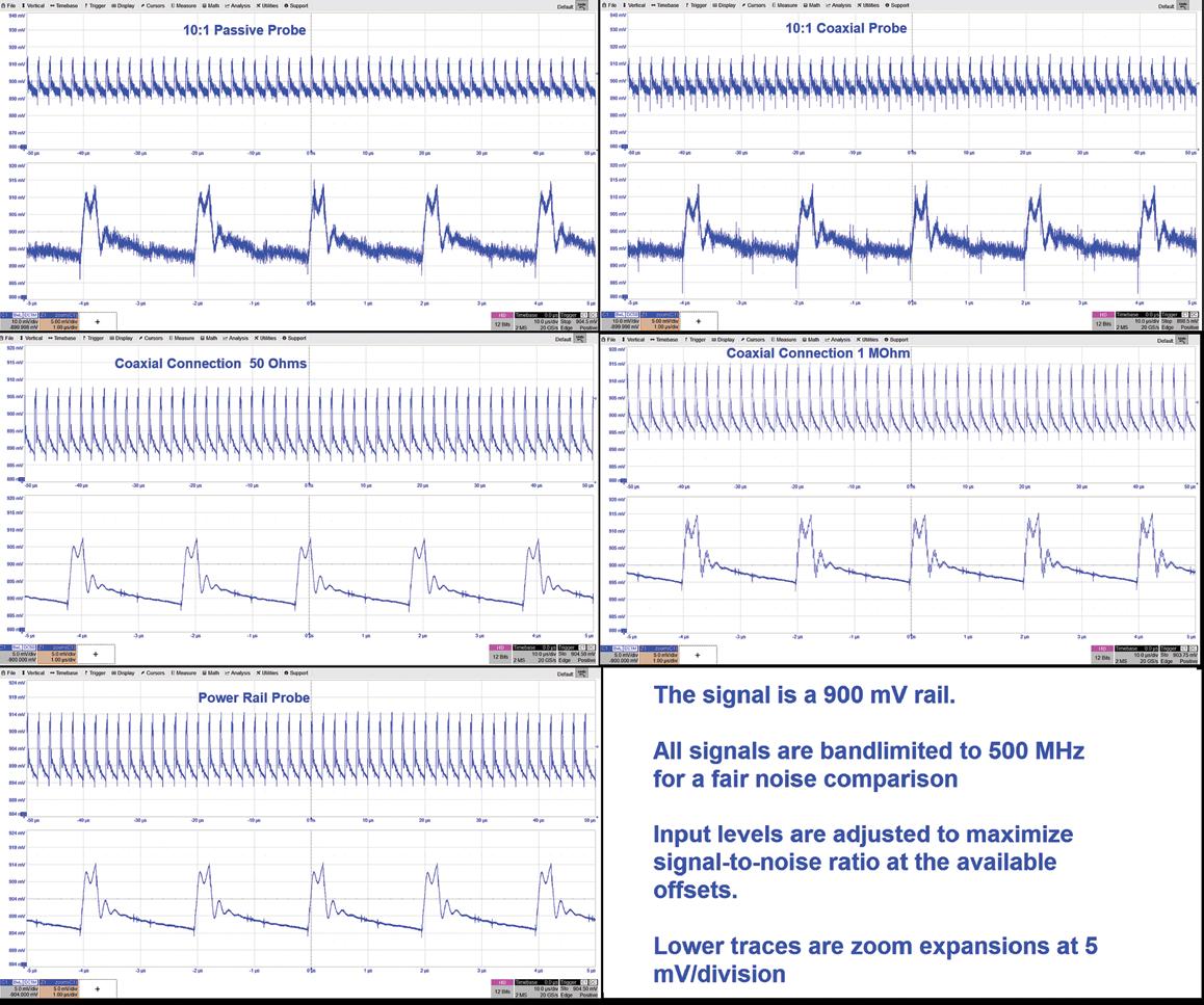
best signal integrity. Both 10:1 probes show additive broadband noise, as expected. The coaxial connection terminated into 1 MΩ shows the reflections of the fast edges due to the impedance mismatch.
Although the 50 Ω terminated coaxial connection produces excellent results at 900 mV, it has a limited offset range (requiring sufficient offset to be available in the oscilloscope) and potential loading issues due to its low impedance. If, however, the oscilloscope has sufficient internal offset and circuit loading is not a concern, this is a very low-cost and high-performance solution to probing a power rail.
A summary of the probing options for power-integrity measurements appears in Table 1. With attention to specific situations, you can use any of these probing methods for powerintegrity measurements. The power-rail probe offers the best performance under almost all conditions. Unfortunately, it's also the highest cost.
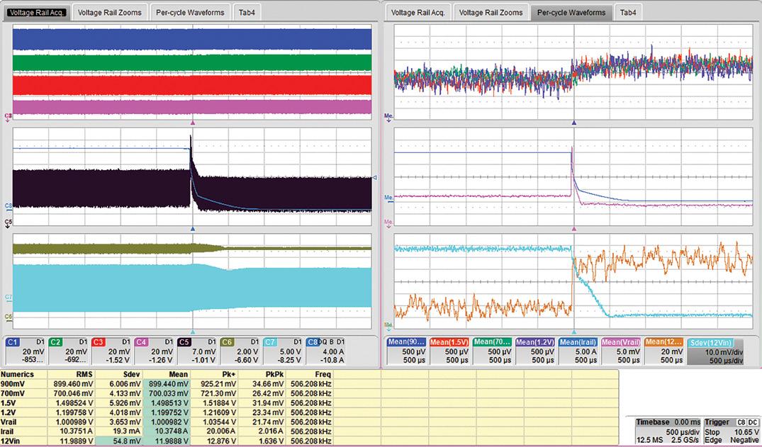
Many oscilloscope manufacturers also offer specialized power integrity software to simplify the measurements, such as that shown in Figure 6.
These software packages capture power rail signals over thousands of switching periods and display statistical data values of the necessary measurements. They also perform a cycle-bycycle analysis of the rail voltages and plot the changes in rail voltage over time as per-cycle waveforms. This vividly displays the behavior of the power rails in a highly intuitive and useful manner.
Recommendations for making power-integrity measurements are listed below:
∙ Remember that it's easy to make a measurement, but it is hard to make a measurement without artifacts.
∙ Know the capabilities and limitations of the probe you choose to use.
∙ If you chose to use a 10:1 probe, remember to use the low inductance tips and adaptors.
∙ For the best performance, use a power rail probe if cost is not an issue. •
Making an accurate ripple measurement with an oscilloscope on a 1 V power rail with a 2% tolerance can be difficult. An oscilloscope's noise floor can get in the way. You can, though, make fast and accurate powerintegrity measurements with oscilloscopes using hardware and software tools.
Noise comes not only from the oscilloscope but from probes and probing accessories. Most oscilloscope manufacturers publish typical RMS noise values for specific models. Figure 1 shows a typical oscilloscope measurement of a DC power rail. You can see the noise, which is a characteristic, not a specification, of the oscilloscope. Moreover, manufacturers only publish typical RMS noise values, but peak-to-peak noise values matter for accurate ripple measurements.
Start by checking the instrument and the accessories that you will use for the measurement instead of relying on published values. A quick characterization takes just a few minutes and requires no external equipment. Disconnect all inputs from the front of the oscilloscope, turn on a peak-topeak (VPP) measurement, set the
vertical scale and sample rate that you will use for the proposed measurement, and let the oscilloscope run until it gives a stable and consistent VPP noise value. Noise levels are dependent on the vertical sensitivity setting, the bandwidth setting, and the path selection (50 Ω or 1 MΩ), and will vary slightly from channel to channel on the same oscilloscope.
Vertical scale and bandwidth settings
Noise is a function of an oscilloscope's fullscreen vertical value. Thus, using a more sensitive vertical resolution will reduce the amount of total noise measured. Furthermore, scaling the signal to fill most of the vertical grid space uses more of the oscilloscope’s ADC resolution, making VPP measurements more accurate. Turning on bandwidth limit filters also reduces broadband noise, additionally improving the accuracy of power-rail measurements. There is, however, a trade-off. Higherfrequency anomalies are hidden if you set the bandwidth limiting too low.
What is the right bandwidth to use?
That depends on the signals. While switching speeds in power supplies may be at kilohertz or low megahertz frequencies, fast edges produce harmonics that can go high into the megahertz range. Higher frequency coupled signals, including clock harmonics, need more bandwidth to capture these higher frequencies. Figure 2 shows noise in the time domain and its frequency distribution.
All major oscilloscope manufacturers offer power-rail probes that incorporate several attributes to make them superior to standard probes. Power-rail probes let you make accurate measurements on small voltages with tight tolerances. This includes the probes’ minimal DC loading impact on the power rail, built-in offset to take advantage of small vertical scaling, and a 1:1 attenuation ratio to minimize noise. Probing power rails with a direct SMA or soldered 50 Ω SMA pigtail coax delivers the lowest noise.
You might be tempted to use the everreadily-available passive probes that ship standard with oscilloscopes for power rail measurements. These probes have a 10:1 attenuation ratio and hence will produce roughly ten times more noise than a 1:1 probe.
If you choose to make a quick measurement using a passive probe across the blocking capacitor, then use a ground that minimizes ground loop area, such as a ground spring. Doing so improves measurement accuracy by reducing the long ground loop that picks up noise. Figure 3 shows how soldering a coax cable directly across a bypass capacitor results in the shortest possible ground loop and thus minimizes noise from a probe.
Characterizing power rails typically involves ensuring there are no unwanted signals coupled onto the rail. That's where signal integrity affects power integrity. Using an
Today’s electronic devices with fast FPGAs, ASICs, and other ICs rely on ever-smaller power rail voltages with tight tolerances. Engineers who incorporate these ICs into their systems need to use oscilloscopes, probes, and measurement techniques that align with today’s tight voltage rail tolerances.
Joel Woodward, Rohde & SchwarzFigure 1. Noise is the largest contributor to inaccuracies in DC rail ripple measurement. Choose a scope, vertical setting, and probing that minimizes measurement noise.
oscilloscope’s spectrum analysis provides a much better method than looking at the rail waveform in the time domain.
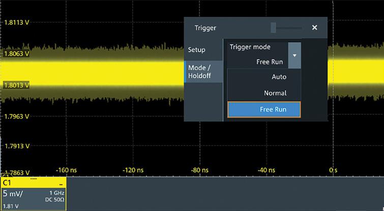
As rail voltage is directly related to the rail’s impedance response, evaluating both signal integrity and power integrity in the frequency domain can shed light on the relationship. Required bandwidth for frequency domain views depends on the potential signals including clocks and potential emissions that may couple onto the power rail. Coupled signals tend to pop out in the frequency domain.
Try looking at the signal integrity and power integrity relationship. A power rail is typically shown as a flat waveform where you measure the peak-to-peak voltage. For clock signals, you often measure jitter. In the time domain, these two elements don’t appear to have a direct relationship. The relationship gets interesting when you look at clock jitter and rail voltage independently in the frequency domain. Plotting a loglog spectrum of the power-rail voltage shows that most of the energy is at lower frequencies as shown in Figure 4. This relates to the impedance of the rail.
Oscilloscopes measure a clock signal's jitter by comparing the rise and fall times of each clock period, or time-interval error (TIE). The oscilloscope can plot this
value, from which you can then apply a log-log spectrum to the TIE measurement. Remarkably, the spectrum of the clock’s TIE and the spectrum of the power rail voltage match shape almost identically. Changes to the power-rail impedance will show equally for both the clock’s TIE spectrum and the power rail-voltage spectrum at similar frequencies.
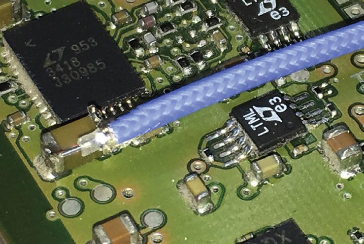
Finding the worst-case amplitudes is a key element of measuring power rails. Getting high-confidence results often necessitate hundreds or thousands of measurements across an extended time window. Power integrity is all about finding outliers. How much measurement time is needed? More
instrument computes all waveform values and produces a corresponding histogram that shows what vertical values occurred in the waveform and the percentage of acquisition samples at a specific amplitude. In a sense, histograms are very compact representations of waveform amplitude values at each sampled point. The histogram does not retain the detail related to the shape of each waveform, but rather just the vertical values. This is exactly what is needed for powerintegrity measurements.
measurement increase confidence.
Unlike just about any other oscilloscope measurement, power integrity doesn't require a trigger. Many oscilloscopes incorporate a less common trigger mode known as free run (Figure 5). With the trigger set to free-run mode, the oscilloscope captures data, processes the data, and captures the next acquisition without waiting for a trigger event. The trade-off is that the acquisition won't occur at the same point of the waveform each time. It's not needed. Free-run trigger mode yields a waveform update rate dramatically faster than in auto or normal trigger modes.
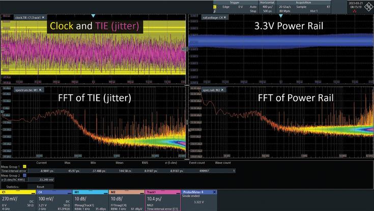
Many oscilloscopes offer a less commonly known feature called waveform histogram (Figure 6). The
Why should you use a histogram? For voltage tolerance testing, the shape of the waveform is not important, but the minimum and maximum values matter. Ripple, noise, and disturbances present themselves as anomalies that exceed voltage-tolerance levels. A histogram is a great visualization tool to see if tolerance levels have been violated.
With waveform histograms, oscilloscopes can measure 20 times faster than using a VPP measurement on each acquisition.
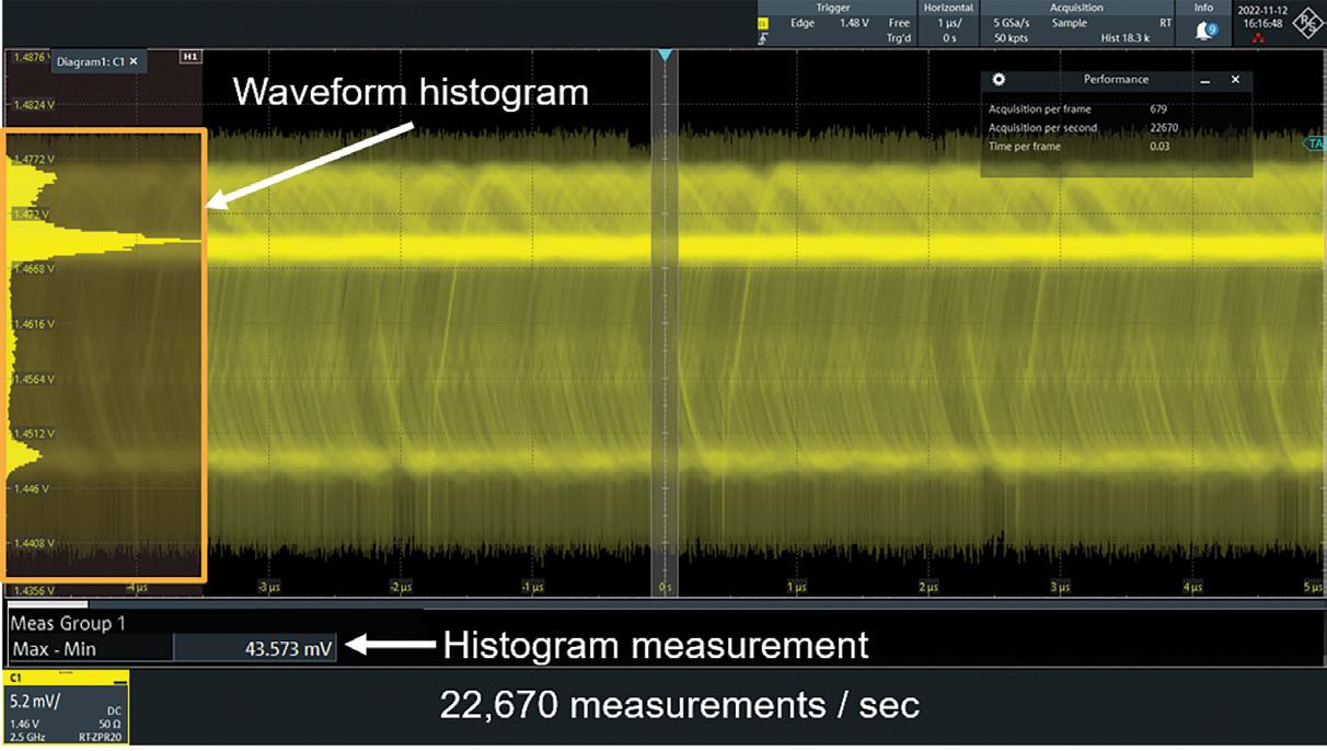
Industry dynamics drive decreases in rail voltage values and tighter tolerances. Choosing the right equipment and applying techniques to reduce measurement noise and speed testing makes the task more accurate and faster. •
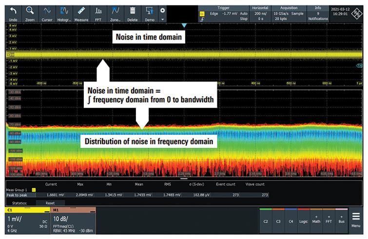
Noise measurement, LO substitution, receiver stress testing, power measurement, CCDF and PAPR characterization, and antennapattern measurement play critical roles in link budget, bit-error rate, and SNR requirements.
Low-Earth orbit (LEO) satellite systems are being deployed for mission-critical use cases at an accelerating rate. This brings associated critical test requirements that, if not performed accurately, could lead to degraded system performance. Using a gateway as an example, this article looks at measurements and the type of equipment required for uplink and downlink physicallayer testing.
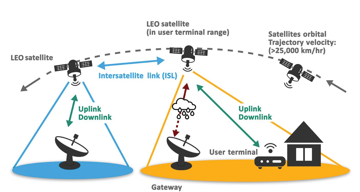
Satellite deployments range from geostationary orbit (GEO) and medium-Earth orbit (MEO) to LEO. Deployment rates of LEO satellites keep increasing. For example, the SpaceX Starlink system currently has approximately 3,500 satellites in low Earth orbit. In December 2022, the FCC approved the deployment of 7,500 next-generation satellites [1]. Due to the low latency of LEO systems, they are becoming the system of choice for both civil and military applications including, but not limited to, 5G and military battlefield communications. Ukrainian use of the Starlink system, although limited, is a recent example of the latter. The use of LEO
Bob Buxton, Wireless Telecom Groupsystems for these types of operations leads to a requirement for high-accuracy testing to ensure reliable operation.
Ground stations, also referred to as gateways when connecting to the terrestrial network, are a key element of uplink and downlink operation, as shown in Figure 1. The various modules comprising the uplink and downlink paths require a variety of tests to ensure reliable operation. Such testing may be performed during the development and production of the modules, during integration, as part of fault-finding, and during operational monitoring. Figure 2 shows a simplified block diagram of the RF and microwave paths in a gateway and examples of where test equipment would be used to assess physicallayer performance.
Table 1 shows additional information and the importance of performing measurements at the points shown in Figure 2. Next, we’ll look at these use cases in more detail.
Many factors contribute to the performance of satellite uplinks and downlinks and several of them, such as the signal purity of the local oscillators, impact bit errors. Excessive phase noise increases error vector magnitude (EVM) and can lead to symbol and hence bit errors because the position of the constellation points on the I-Q diagram cross over symbol decision boundaries as shown in Figure 3.
When making this measurement, ask yourself if you need to make absolute phasenoise measurements of the local oscillator (LO) to measure additive noise from amplifiers.
Phase noise measurement
Local oscillator (LO) substitution
During development to ensure the spectral purity of the designed-in local oscillators meet specifications.
During development or fault-finding to diagnose a problem in a upconverter or downconverter, or when designed-in LO is not available.
Phase noise analyzer
High performance synthesizer
Reduce likelihood of poor phase noise causing bit errors
Fix issues prior to deployment
Receiver stress testing
During development to ensure correct operation of the receiver in the presence of noise or other interference.
Programmable noise generator or signal-to-noise generator, signal source, BERT, and test loop translator
Ensure signals can be received to meet the required BER under poor signal/noise conditions
Output power
Gain and gain compression
During development of power amplifiers and upconverters. Also measured for monitoring during operational use.
Peak power sensor and meter
Ensure power level is sufficient to meet requirements of link budget
During development of power amplifiers. Peak power sensor and meter
Antenna Pattern measurement During development
LO substitution is an important technique when testing upconverters and downconverters in communication systems. It lets you evaluate signal chains without the characteristics of the LO masking their performance. This technique also lets you determine if the LO is the source of issues when the system is not performing properly.
Whether in a gateway or in a satellite, it is important to stress test the receiver to ensure that signals can be received and demodulated correctly under impaired conditions. To ensure performance observed in the lab is replicated after deployment, satellite communication receivers must operate in real-world RF interference
conditions. These tests are performed at IF and at RF.
When performed at IF, you will need:
∙ Signal-to-noise ratio (SNR) noise generator to set levels of either SNR or Eb/No
∙ Bit error rate tester (BERT).
The uplink IF is looped back to the downlink IF through the SNR generator. If the testing is at RF/microwave frequencies, a test loop translator will also be needed to complete the loop back. Figure 4 shows the general test setup for the two cases.
To perform the test, the SNR generator adds a precise amount of noise to produce the desired SNR level. The level of noise is increased until the desired error rate limit, as monitored by the BERT, is reached. Additionally, a signal generator may be used to inject an interfering signal.
Fast measurement RF/ microwave power sensor and meter
This brings us to one of the most fundamental RF and microwave measurements: power. Power measurement can also uncover some critical issues that could impact system performance.
Figure 5 shows a setup for evaluating the performance of the uplink high-power amplifier (HPA).
In addition to the measurement of gain and return loss, power sensor P2 provides
Avoid amplifiers in compression clipping signal peaks and causing bit errors
Ensure gain and main beam directivity meets requirement of link budget and beam positioning works correctly
a measure of the output power level. You can also use this setup to assess the degree of signal compression being caused by the HPA.
Historically, satellite links have used low peak-to-average power ratio (PAPR) modulation formats. Newer applications, such as 5G non-terrestrial networks (NTN), however, require the use of higher-order modulation schemes and OFDM [2]. This means that the PAPR of the signal will be higher, and
it will be necessary to take care that amplifier compression does not distort the peaks leading to symbol and hence bit errors. There have been several studies of the effect of PAPR reduction on bit error rate due to signal compression. A study by Usman et al showed that reducing the PAPR from 10 dB to ~4dB would degrade the BER from ~8 x 10⁻⁴ to ~1.3 x 10⁻³ for an SNR of 10 dB at the receiver [3]. This highlights the importance of knowing the impact of power-amplifier distortion on PAPR and of having a means to clearly observe it.
You can assess amplifier non-linearity and compression using average-detecting power sensors or network analyzers
to get a plot of POUT vs PIN This does not, however, reveal the impact on the PAPR of a complex m-QAM OFDM signal. Fortunately, there is a simple solution that you can apply. This is to use high sample rate peak power sensors with video bandwidth that is wider than the signal channel being measured. Those power samples are used to determine the signal PAPR and plot complementary distribution function (CCDF) curves. A CCDF curve is a plot of the probability of a modulated signal exceeding a specific PAPR. The setup is simple and uses power sensors P1 and P2 shown in Figure 6; the sensors must measure peak and not just average power. Using those sensors, together with the appropriate analysis software, provides the CCDF at the input and output of the amplifier thus revealing the PAPR reduction.
Figure 6 shows this result using peak power sensors and power analyzer software. The y-axis shows the probability of exceeding the PAPR level indicated on the x-axis. Figure 6 shows that 99.99% of the time, the input signal has a PAPR of
~9.4 dB while the amplifier compression reduced the output signal PAPR to ~7.4 dB, which could lead to bit errors.
Lastly, let’s look at antenna pattern measurement. Whether the antenna is a mechanically steered dish or an electronically steered phased-array panel with multi-beam spatial multiple access capability and the ability to point nulls towards interferers, you must characterize the antenna pattern. This is usually represented by polar plots in azimuth and inclination planes. Power sensors provide a simple and convenient way to make these measurements.
The antenna is mounted on a turntable. One power sensor is coupled to its feed monitoring the transmit power level to ensure it remains constant during the antenna rotation. A second power sensor, coupled to a standard-gain horn, is in the antenna's far field. The measurements taken from this power sensor are used to produce the antenna pattern plots. To have an optimum combination of angular resolution and speed of measurement, it is desirable to choose a power sensor that provides a fast measurement rate.
We’ve touched on several key physical-layer measurements that help to provide confidence that the individual system blocks and the overall system, when deployed, will perform reliably. The measurement techniques presented here do not only apply to gateways. You can apply similar techniques to terminals and satellites. •
[1] https://www.fcc.gov/ document/fcc-partially-grantsspacex-gen2-broadbandsatellite-application
[2] ETSI Technical Specification
TS 138 211 V17.1.0 Physical channels and modulation
[3] Usman et al, PAPR reduction and digital predistortion for 5G waveforms in digital satellite payloads. Advances in Communications Satellite Systems. 37th International Communications Satellite Systems Conference (ICSSC-2019).
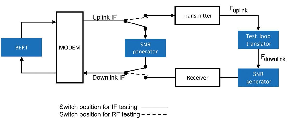
Jami Brownlee jbrownlee@wtwhmedia.com 224.760.1055
Jim Dempsey jdempsey@wtwhmedia.com 216.387.1916
Mike Francesconi mfrancesconi@wtwhmedia.com 630.488.9029
Customer Service Manager Stephanie Hulett shulett@wtwhmedia.com
Customer Service Representative Tracy Powers tpowers@wtwhmedia.com
Customer Service Representative
Trinidy Longgood tlonggood@wtwhmedia.com
WTWH Media, LLC 1111 Superior Ave., Suite 2600 Cleveland, OH 44114
Ph: 888.543.2447
FAX: 888.543.2447
Courtney Nagle cseel@wtwhmedia.com 440.523.1685
Jim Powers jpowers@wtwhmedia.com 312.925.7793
Publisher Mike Emich memich@wtwhmedia.com 508.446.1823
Managing Director Scott McCafferty smccafferty@wtwhmedia.com 310.279.3844
EVP
Marshall Matheson mmatheson@wtwhmedia.com 805.895.3609
Customer Service Representative JoAnn Martin jmartin@wtwhmedia.com
Customer Service Representative Renee Massey-Linston renee@wtwhmedia.com
DESIGN WORLD does not pass judgment on subjects of controversy nor enter into dispute with or between any individuals or organizations. DESIGN WORLD is also an independent forum for the expression of opinions relevant to industry issues. Letters to the editor and by-lined articles express the views of the author and not necessarily of the publisher or the publication. Every effort is made to provide accurate information; however, publisher assumes no responsibility for accuracy of submitted advertising and editorial information. Non-commissioned articles and news releases cannot be acknowledged. Unsolicited materials cannot be returned nor will this organization assume responsibility for their care.
DESIGN WORLD does not endorse any products, programs or services of advertisers or editorial contributors. Copyright© 2022 by WTWH Media, LLC. No part of this publication may be reproduced in any form or by any means, electronic or mechanical, or by recording, or by any information storage or retrieval system, without written permission from the publisher.
SUBSCRIPTION RATES: Free and controlled circulation to qualified subscribers. Non-qualified persons may subscribe at the following rates: U.S. and possessions: 1 year: $125; 2 years: $200; 3 years: $275; Canadian and foreign, 1 year: $195; only US funds are accepted. Single copies $15 each. Subscriptions are prepaid, and check or money orders only.
SUBSCRIBER SERVICES: To order a subscription or change your address, please email: designworld@omeda.com, or visit our web site at www.designworldonline.com
POSTMASTER: Send address changes to: Design World, 1111 Superior Ave., Suite 2600, Cleveland, OH 44114
Today’s electronic engineers are challenged by multiple factors. Research over the years has illustrated common trends that you, as engineers, deal with including keeping your skills up-to-date, shrinking time-to-market windows, fewer engineers and smaller design teams for large projects and evolving technological trends. The bottom line is that you must continually update your engineering knowledge base to be successful in your work.


Throughout 2023, we are presenting a series of online educational days where you can learn how to address specific design challenges, learn about new techniques, or just brush up your engineering skills. We are offering eight different Training Days. Each day will focus on helping you address a specific design challenge or problem. These are not company sales pitches! The focus is on helping you with your work.
AVAILABLE ON DEMAND THERMAL MANAGEMENT
JUNE 14TH DESIGNING FOR SUSTAINABILITY
JULY 12TH EMI/RFI/EMC
AUGUST 9TH BATTERY MANAGEMENT
SEPTEMBER 13TH MOTOR DRIVES DESIGN
OCTOBER 11TH IOT DESIGN / WIRELESS
For more information and to register for these webinars, go to:
EETRAININGDAYS.COM
NOVEMBER 8TH ELECTRIC VEHICLE DESIGN
DECEMBER 6TH 5G / RF DESIGN
All-new features
• 4:1 test TUR for most popular 6.5-digit multimeters
• 30 A continuous current output to extend AC/DC measurement ranges
• Calibrate AC/DC voltage, current, resistance, capacitance, and inductance
• Automated with MET/CAL™ Calibration Management Software

• 7-inch color touch screen
A family of multi-product calibrators designed to match your electrical workload