Mouser Electronics offers a vast selection of over 6.8 million products from more than 1200 leading manufacturers. As a global authorised distributor, Mouser empowers engineers and procurement professionals by providing seamless access to the latest semiconductors and electronic components, enabling them to accelerate their design processes. With Mouser’s ‘no minimum order quantity’ policy, customers can order just one or countless other components to fulfil all their exact design requirements, fully meeting the demands of Fortune 500 companies, startups, inventors and universities. The company’s website hosts an extensive library of technical resources, including product data sheets, design tools, reference designs and application notes, giving customers the tools they need to explore new possibilities and create innovative solutions. Mouser’s commitment to customer satisfaction is reflected in its global support network and state-of-the-art distribution facilities, providing fast and reliable service. Focused on delivering high-quality products and expert technical support, Mouser is a trusted partner for engineers and innovators across a variety of industries. Go and instantly access an entire world of semiconductors and electronic components at au.mouser.com — in stock, ready to ship.
Mouser Electronics au.mouser.com
MOUSER ELECTRONICS:
CONNECTIVITY — EVER-INCREASING POSSIBILITIES
Initially, efforts aimed at implementing the 5G network were met with a dose of resistance and doubt from society. However, with time, more and more users have started taking advantage of this new technology.
It supports rapid mobile data transmissions and connections spanning a huge number of various devices, including environmental sensors or units detecting specific events or objects. This, in turn, facilitates forecasting, monitoring, remote control and other operations that were previously inaccessible or even impossible due to the technological limitations of wireless networks.
Initially, the implementation of the 5G transmission technology was based on the formerly used 4G LTE technology, and it involved deploying software updates in base stations. However, this solution made it rather hard to make use of the full potential of 5G, and its main effect was on marketing and advertising the new network. That being said, it must also be admitted that it did offer some advantages over LTE. Firstly, the transmission speed was increased, and secondly, the network capacity was enhanced without any physical infrastructure expansion. Instead, now that the ‘old’ infrastructure has been in place for some time, higher carrier frequencies (“C” band) are used to allow transmission speeds reaching several gigabits per second.
The 5G network is even capable of operating one million devices within a 1 km2 area. This capability has an enormous impact on
the development of IoT, smart city, modern agriculture, Industry 4.0 and other applications, such as illumination and water supply management systems, road traffic intensity analysis software, and programs running car parks or supervising autonomous vehicle operation. Moreover, thanks to the impressive network capacity, devices not only transmit data to the system that supervises their operation or creates forecasts, but also communicate with one another. Even today, solutions implemented in some autonomous vehicles make it possible to share data on accidents, traffic jams and detours. There are also solutions that are able to control traffic lights depending on actual traffic, thus eliminating congestion.
5G technology — basic overview
The main spectrum of radio frequencies operated in 5G networks ranges from 3.3–4.9 GHz. Lower frequency bands (<1 GHz) are reserved for devices providing larger area coverage and designed to penetrate rooms. Millimetre waves (frequency range: from 24–28 GHz and 39 GHz) are used in local hot-spots and applications providing outdoor and indoor connectivity. The 5G network radio frequency interface has been developed in a manner ensuring maximum flexibility, as it
makes it possible to combine waves from various frequency ranges.
Other important features of the new interface include MIMO technology and antenna array deployment. The antennas (also referred to as Massive MIMO) are installed in base stations to facilitate not only the correct forming of the frequency characteristics, but also of the radiation characteristics, to ensure the area has coverage and direct radio frequency beams away from the user’s head (in mobile devices). As such, the MIMO antennas made it possible for the LTE and 5G technologies to ‘coexist’ within the same area during the initial stages of the implementation process.
The 5G radio network includes the ORAN (Open Radio Access Network) interface operating between the RF path and cloud edge devices. It facilitates flexible service deployment and provides access to cloud resources and services. The processing operations required for correct radio frequency path functioning are performed by cloud edge devices, ensuring that the network capacity is quickly adapted to actual requirements.
The LTE networks support the following modulation schemes: QPSK, 16QAM, 64QAM and 256QAM. All the above-mentioned modulation types are also used by the 5G network radio frequency interface. Moreover,
the 3GPP specification also includes the n/2BPSK scheme to facilitate further reduction of the peak-to-medium power ratio at low transmission speeds, which is important in the context of selected services.
This feature is particularly useful while collecting data obtained from IoT sensors. The power ratio reduction in wireless paths provides energy savings to ensure longer operation of battery-operated equipment. A lower peak power rating may enhance network performance and mitigate the risk of interferences, which translates into higher connection quality and reliability. This is particularly important in areas characterised by high density of devices. Additionally, the peak power reduction ensures more efficient use of the available frequency resources (decreased harmonic levels), which in turn translates into higher network capacity, ie, the ability to simultaneously operate a larger number of connected devices.
The spectrum of the new 5G network applications is even more extensive, so the list of modulation schemes is likely to be extended as well. For example, the 1024QAM modulation scheme may become part of the radio frequency interface specification, as the fixed connection designed to transmit data from the main network to sub-networks already uses a
higher modulation scheme than 256QAM. The radio frequency interface specifications may also include modulation schemes dependent on the terminal equipment.
For the operation of diverse services within a broad frequency range, the scalable OFDM technology is required. It involves multiplexing in the frequency domain, ie, a simultaneous transmission of multiple data streams using orthogonal carrier frequencies. Wider carrier spacing may be available for small-area, highcarrier-frequency services, where latency is a key factor. If individual carrier frequencies are lower, the spacing among them can be decreased, which is particularly useful for large-area services, narrow-band equipment and multimedia services, eg, eMBMS. It may also be possible to simultaneously support multiple services with different requirements using the same carriers by multiplexing two different channel splits.
5G — main assumptions
The 5G network architecture has been designed with a view to operating the following three key service areas:
Enhanced mobile broadband (eMBB) connectivity: This service area extends and enhances the services currently used in mobile data transmission applications. It
ensures the 10 Gb/s transmission rates for high-throughput applications, such as video streaming or VR/AR gaming.
Massive machine-type communications (mMTC): This service is designed to connect a massive number of devices. It is expected to be used mainly in applications related to smart city solutions and other IoT applications.
Ultra-reliable low latency communications (URLLC): URLLC is a perfect solution for critical applications which require network reliability, minimum latency (below 1 ms), and short response times. Such applications include autonomous vehicles or remote control systems for industrial machinery.
Enhanced mobile broadband (eMBB)
Initially, during the process of the 5G implementation, emphasis was put mainly on multiplying the data transmission speeds to enhance the mobile broadband application capabilities.
The 5G technology makes it possible to obtain very high transmission rates, due to the fact that broadband transmissions supported by the MIMO technology are implemented. The typical maximum bandwidth for the carrier frequency below 1 GHz is 20 MHz, which translates into 200 Mb/s TDD (time-division duplex) speeds at 2×2 MIMO. The 100 MHz TDD band and 4×4 MIMO application provide transmission rates even up to 2 Gb/s. Also, 24–28 GHz frequency range millimetre waves make it possible to obtain 10–20 Gb/s at the 1 GHz bandwidth and 2×2 as well as 4×4 MIMO.
Thanks to the implementation of the 5G technology in existing LTE networks, much larger network capacities and higher data transmission speeds were obtained, mainly as a result of using antenna matrices and the MIMO technology. In real-life networks, an LTE cell with 20 MHz bandwidth ensures throughput amounting to 40 Mb/s, at medium-level traffic intensity. A 5G network cell with 100 MHz bandwidth makes it possible to connect 20 times more users, as a 5 times broader frequency band is used. So far, the 5G technology has ensured the highest capacity increase in the history of mobile telephony networks.
mMTC = millions of connected devices
Massive machine-type communications facilitates transmission of massive numbers of small-sized data packages (eg, sensor data) to/from a large number of devices. mMTC streamlines using applications collecting IoT sensor data to enhance the quality of users’ life or services they provide.
iStock.com/Jian Fan
NOVEL BIOSENSOR INCREASES ELEMENT EXTRACTION EFFICIENCY
QUT synthetic biologists have developed a prototype for an innovative biosensor that can detect rare earth elements and be modified for a range of other applications.
Lanthanides (Lns) are elements used in electronics, electric motors and batteries. The problem is that we can’t extract enough of them to meet the growing demand and current extraction methods are expensive and environmentally damaging.
Professor Kirill Alexandrov and colleagues, from the QUT Centre of Agriculture and Bioeconomy and the ARC Centre of Excellence in Synthetic Biology, engineered proteins to create molecular nanomachines that generate easily detectable signals when they selectively bind to Lns.
Along with Professor Alexandrov, the international research team involved QUT researchers Dr Zhong Guo, Patricia Walden and Dr Zhenling Cui, in collaboration with researchers from CSIRO Advanced Engineering Biology Future Science Platform and Clarkson University (USA).
Publishing their findings in Angewandte Chemie International, the team describe engineering a hybrid protein, or “chimera,” by combining a lanthanide-binding protein, LanM, with an antibiotic degrading enzyme called beta-lactamase.
HARNESSING ELECTROMAGNETIC WAVES TO IMPROVE WIRELESS COMMUNICATION
A team of researchers from the University of Ottawa has developed innovative methods to enhance frequency conversion of terahertz (THz) waves in graphene-based structures, unlocking new potential for faster, more efficient technologies in wireless communication and signal processing.
THz waves, located in the far-infrared region of the electromagnetic spectrum, can be used to perform non-invasive imaging through opaque materials for security and quality control applications. Additionally, these waves hold great promise for wireless communication. Advances in THz nonlinear optics, which can be used to change the frequency of electromagnetic waves, are essential for the development of high-speed wireless communication and signal processing systems for 6G technologies and beyond.
THz technologies are rapidly evolving as they are poised to play a critical role in health, communication, security and quality control. Jean-Michel Ménard, Associate Professor of Physics from the Faculty of Science and a team of researchers have paved the way for developing devices capable of up-converting electromagnetic signals to higher oscillation frequencies, effectively bridging the gap between GHz electronics and THz photonics.
These findings — published in Light: Science & Applications — demonstrate innovative strategies for enhancing THz nonlinearities in graphene-based devices. “The research marks a significant step forward in improving the efficiency of THz frequency converters, a critical aspect for multi-spectral THz applications and especially the future of communication systems, like 6G,” said Ménard, who collaborated on the project with fellow uOttawa researchers Ali Maleki and Robert W. Boyd.
lanthanides are present. It can be used to detect and quantify Lns in liquids, producing a visible colour change or an electrical signal.
Impressively, bacteria modified with these chimeras were able to survive in the presence of antibiotics that otherwise would kill them — but only when lanthanides were present. This highlights how precisely the proteins respond to these rare metals.
“This work opens up exciting possibilities for using biology to detect and recover rare earth metals,” Professor Alexandrov said.
“The prototype can also be modified for various biotechnological applications, including construction of living organisms capable of detecting and extracting valuable metals.”
The research team now plan to work on increasing the specificity of the molecular switch to better differentiate between closely related rare earth elements. It also explores the possibility of developing switches for other critical elements. The team is in active discussions with potential industry partners who are interested in this technology.
“We also want to explore using the tool to engineer microbes that can directly extract rare earth minerals from ocean water,” Alexandrov said.
“This is probably one of the best performing switches made and has given us a lot of insight into the mechanics of protein switches.”
This new research showcases methods to leverage the unique optical properties of graphene, an emerging quantum material made of a single layer of carbon atoms. This 2D material can be seamlessly integrated into devices, enabling new applications for signal processing and communication.
Previous works combining THz light and graphene primarily focused on fundamental light–matter interactions, often examining the effect of a single parameter in the experiment. The resulting nonlinear effects were extremely weak. To overcome this limitation, Ménard and his colleagues have combined multiple innovative approaches to enhance nonlinear effects and fully leverage graphene’s unique properties.
“Our experimental platform and novel device architectures offer the possibility to explore a vast range of materials beyond graphene and potentially identify new nonlinear optical mechanisms,” added Maleki, a PhD student in the Ultrafast THz group at uOttawa, who collected and analysed results for the study.
“Such research and development are crucial for refining THz frequency conversion techniques and eventually integrating this technology into practical applications, particularly to enable efficient, chip-integrated nonlinear THz signal converters that will drive future communication systems.”
Image credit: QUT.
Conceptual artwork of a biosensor.
IMPROVING THE WAY FLASH MEMORY IS MADE
The right recipe creates the narrow, deep holes needed for dense data storage twice as fast. To store ever more data in electronic devices of the same size, the manufacturing processes for these devices need to be studied in greater detail. By investigating new approaches to making digital memory at the atomic scale, researchers engaged in a public-private partnership are aiming to address the endless demand for denser data storage.
One such effort has focused on developing the ideal manufacturing process for a type of digital memory known as 3D NAND flash memory, which stacks data vertically to increase storage density. The narrow, deep holes required for this type of memory can be etched twice as fast with the right plasma and other key ingredients, according to a new study published in the Journal of Vacuum Science & Technology A . The study involved simulations and experiments conducted by scientists at Lam Research, the University of Colorado Boulder and the U.S. Department of Energy’s Princeton Plasma Physics Laboratory (PPPL).
NAND flash memory is a type of non-volatile data storage, meaning that it retains data even if the power to the device is off. “Most people are familiar with NAND flash memory because it’s the kind that is in the memory cards for digital cameras and thumb drives. It is also used in computers and mobile phones. Making this type of memory denser still — so that more data can be packed into the same footprint — will be increasingly important as our data storage needs grow due to the use of artificial intelligence,” said Igor Kaganovich, a principal research physicist at PPPL.
Stacking memory cells to save space
Digital memory saves information in units called cells. Data is saved as the cell’s state, where each cell is either on or off. With traditional NAND flash memory, the cells are arranged in a single layer. In 3D NAND flash memory, many memory cells are stacked on top of each other to fit more data in a smaller footprint. It’s akin to replacing a bungalow with a 10-storey apartment to house more people.
A critical step in creating these stacks involves carving holes into alternating layers of silicon oxide and silicon nitride. The holes can be etched by exposing the layered material to chemicals in the form of plasma (partly ionised gases). Atoms in the plasma interact with atoms in the layered material, carving out the holes.
Researchers want to refine how they make these holes so each one is deep, narrow and vertical, with smooth sides. Getting the recipe just right has been tough, so scientists have continued to test new ingredients and temperatures.
Using plasma to create deep, narrow channels
“These processes use plasma as a source of high-energy ions,” said Yuri Barsukov, a former PPPL researcher now working at Lam Re-
fluoride plasma instead of the separate hydrogen and fluorine gases. While the effect for silicon nitride was more pronounced than for silicon oxide, etching both materials simultaneously yielded the most significant increase. In fact, the etching rate for the alternating silicon oxide and silicon nitride layers more than doubled, increasing from 310 nanometres per minute to 640 nanometres per minute. (A human hair is roughly 90,000 nanometres in width.)
“The quality of the etch seems to have improved as well, and that’s significant,” Lill said.
The researchers also studied the impact of phosphorus trifluoride, an essential ingredient when etching silicon dioxide at any significant degree. While it has been used before, the researchers wanted to better understand and quantify its impact. They found that adding phosphorus trifluoride quadrupled the etch rate for silicon dioxide, though it only marginally increased the silicon nitride etch rate.
search. Using the charged particles found in plasma is the easiest way to create the very small but deep, circular holes needed for microelectronics, he said. However, the process, known as reactive ion etching, isn’t fully understood and could be improved. One recent development involves keeping the wafer — the sheet of semiconductor material to be processed — at a low temperature. This emerging approach is called cryo etching.
Traditionally, cryo etching uses separate hydrogen and fluorine gases to make the holes. The researchers compared results from this process to a more advanced cryo-etching process that uses hydrogen fluoride gas to create the plasma.
“Cryo etch with the hydrogen fluoride plasma showed a significant increase in the etching rate compared to previous cryo-etch processes, where you are using separate fluorine and hydrogen sources,” said Thorsten Lill of Lam Research. Headquartered in Fremont, California, Lam Research supplies wafer fabrication equipment and services to chipmakers.
Doubling etch rates
When silicon nitride and silicon oxide were tested separately, the etch rate increased for the nitride and the oxide layer using the hydrogen
Another chemical compound the researchers studied was ammonium fluorosilicate, which forms during the etching process when the silicon nitride reacts with the hydrogen fluoride. The research showed that ammonium fluorosilicate can slow down etching, but water can offset this effect. According to Barsukov’s simulations, water weakened the ammonium fluorosilicate bonds. “The salt can decompose at a lower temperature when water is present, which can accelerate etching,” Barsukov said.
Laying a foundation for future research
Kaganovich said the research is also important because it shows how scientists in industry, academia and national laboratories can work together to answer important questions in the microelectronics field. It also brings together information gathered from experimentalists and theorists. “We are building bridges to the greater community,” he said. “This is an essential step in gaining a better understanding of semiconductor manufacturing processes for everyone.”
Lill said he appreciates working with PPPL on semiconductor manufacturing research because PPPL research offers a range of capabilities in plasma simulation for microelectronics.
Alternating layers of silicon dioxide and silicon nitride (left) are etched to create a deep, vertical hole (right).
Kyle Palmer/PPPL Communications Department.
iStock.com/lyash01
CIRCUIT DESIGN
then scaled to other circuits, sub-systems and systems, making the design process extremely complex and time consuming, particularly for modern, high-performance chips behind applications like wireless communication, autonomous driving, radar and gesture recognition.
“Classical designs carefully put these circuits and electromagnetic elements together, piece by piece, so that the signal flows in the way we want it to flow in the chip. By changing those structures, we incorporate new properties,” Sengupta said. “Before, we had a finite way of doing this, but now the options are much larger.”
It can be hard to comprehend the vastness of a wireless chip’s design space. The circuitry in an advanced chip is so small, and
the geometry so detailed, that the number of possible configurations for a chip exceeds the number of atoms in the universe, Sengupta said. There is no way for a person to understand that level of complexity, so human designers don’t try. They build chips from the bottom up, adding components as needed and adjusting the design as they build.
The AI approaches the challenge from a different perspective, Sengupta said. It views the chip as a single artefact. This can lead to strange but effective arrangements. He said humans play a critical role in the AI system, in part because that AI can make faulty arrangements as well as efficient ones. It is possible for AI to hallucinate elements that don’t work, at least for now. This requires some level of human oversight.
“There are pitfalls that still require human designers to correct,” Sengupta said. “The point is not to replace human designers with tools. The point is to enhance productivity with new tools. The human mind is best utilised to create or invent new things, and the more mundane, utilitarian work can be offloaded to these tools.”
The researchers have used AI to discover and design complex electromagnetic structures that are co-designed with circuits to create broadband amplifiers. Sengupta said future research will involve linking multiple structures and designing entire wireless chips with the AI system.
“Now that this has shown promise, there is a larger effort to think about more complicated systems and designs,” he said. “This is just the tip of the iceberg in terms of what the future holds for the field.”
The AI design features unusual, and efficient, circuitry patterns.
Emir Ali Karahan, Princeton University.
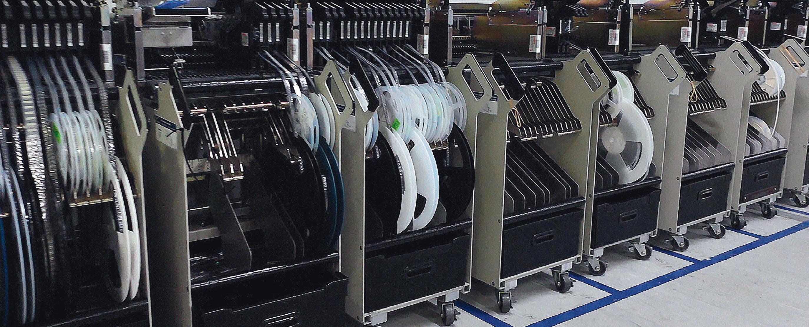
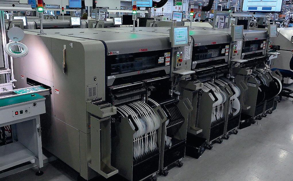
start a product in Australia or New Zealand and then transfer the product to China. The Yamahas have been integral in making that transfer process very easy.
Having four identical lines in Australia gives us great capacity and flexibility. We can run any product on any line, there are no planning considerations. Our four lines have three modules in each line, which offers a huge feeder account. We build some products which have over 6,000 parts on a board. We can set up those products to run both sides in the one set-up, so lots of flexibility and capacity.
You have made some significant investments over the years that enable GPC to offer impressive capabilities for Electronics Manufacture. How important is it for you to measure each part of the production process to ensure maximum efficiency and productivity?
We verify the performance of major equipment after we have purchased it. When running a surface mount line, we can see the actual machine output and compare that to what is in our ERP system to see whether we are on track with effi ciency. We also have automatic optical inspection stations at the end of each line, which look at the quality of the product going through. This information feeds back into a real-time SPC chart so we can verify the quality of the product.
We also ensure that the equipment is utilised correctly. With the surface mount equipment, we went through a quick changeover process, looking to optimise all steps in the process.
One of the outcomes was to invest in more surface mount tables, feeders and software. We could do complete offline setups while machines were running other product. When the changeover occurred, it was quite easy just to move the old
tables out, scan new tables to the machines and then we were right to run. We saw huge benefits in that, in the order of 80% reduction in changeovers.
With offices/facilities in Sydney, Christchurch in New Zealand, and Shenzhen in China, how important is it for GPC to draw business from the Australasian market and overseas? Some businesses like to have manufacturing close to where they are located. They can look at the progress of new products, or there may be special security requirements and, therefore, products must be made in a certain location. GPC can support all these options for customers.
GPC can offer manufacturing from a low labour cost market such as China. The advantage with GPC is that we manage all processes locally for the customer. The customer doesn’t have to deal with China directly. They deal with GPC, and we organise the purchasing, planning, and all aspects of the builds.
We have an International Procurement Offi ce in China and do a lot of our purchasing for the group from there. We can also perform quality audits on products before they ship. Noncompliant product is detected before it is shipped to GPC, improving quality and eliminating delays.
Hawker Richardson has been an SMT equipment supplier to GPC for over a decade. How important is it that your suppliers understand your business and your requirements?
Our suppliers must have a very good knowledge of GPC equipment and processes. If we have breakdowns, they need to make sure we are up and running as soon as possible.
In terms of equipment spares, Hawker Richardson identifies which ones are critical and stores them locally so that if something were to happen, we can be up and running very quickly.
Knowing what we currently do means that they provide good solutions for new equipment straight away rather than going through a process where there’s lots of discussion working out what is best for GPC.
Could you share your overall experience with Hawker Richardson’s service and support?
The overall experience with Hawker Richardson is very positive. We have been working together for a long time, and they have very good knowledge of their product. If something happens to their equipment, we know that they will sort it out quickly.
Hawker Richardson is also willing to help in difficult situations. With the recent purchase of surface mount equipment, we were going to have a long delay due to transport issues at the wharf. Hawker Richardson reduced the delay. We moved the equipment off the boat earlier and transported it across land to get it onsite earlier. The machines were up and running quickly.
Would you recommend Hawker Richardson to anyone else based on your experience?
They are easy to deal with, reliable and always on time. Our experiences have been very good over many years. So, very happy to recommend Hawker Richardson.
Hawker Richardson www.hawkerrichardson.com.au
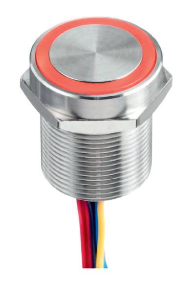
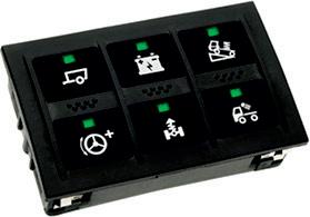
PIEZO ELECTRIC SWITCH
Control Devices has launched a reinforced PBAK series (19 mm diameter) of piezo electric switches. The anti-vandal switches are designed with a stainless steel (316L) body and polycarbonate illumination ring to extend protection. They are sealed to IP69K and can withstand impacts of up to IK06 (equivalent to one joule), with a long life expectancy of up to 50 million cycles.
The switches also feature bright RGB illumination feedback for increased visibility in all types of conditions. The switches are suitable for various outdoor applications such as bike sharing stations, emergency call boxes or parking meters, as well as applications that require impact resistance.
Control Devices Australia www.controldevices.com.au
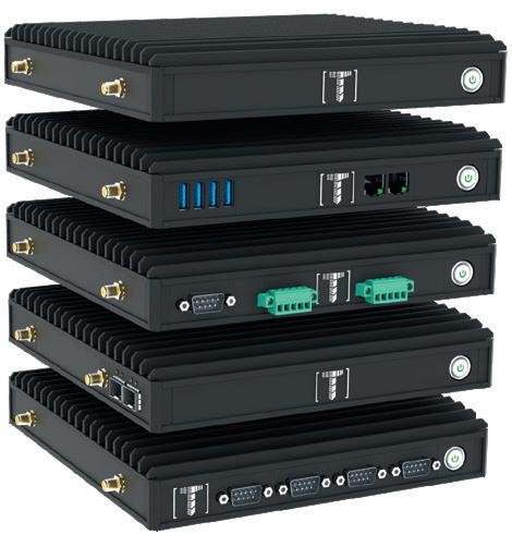
AI ACCELERATION MODULES
MINIATURE DC MOTORS
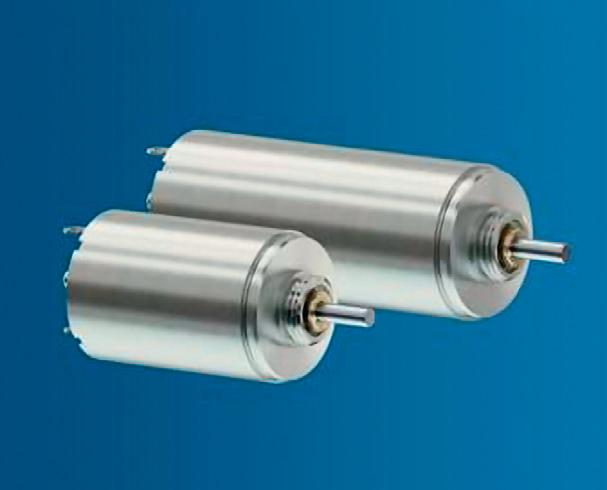
FAULHABER has expanded its DC motor line-up with the 1218 SXR and 1228 SXR; these high-performance miniature motors feature optimised rotor balancing for smooth operation and extended lifespan, making them suitable for precision-driven industries.
The SXR series stands out with its innovative hexagonal coil technology, offering a high copper fill factor and straight wiring for enhanced efficiency. A new magnet grade boosts magnetic induction and temperature stability, providing consistent performance in challenging environments.
With flexible voltage options (3–18 V), multiple bearing configurations and customisation possibilities (including vacuum and high-temperature adaptations), these motors cater to diverse needs. They are RoHS compliant and easily integrate with FAULHABER’s planetary gearheads, like the 14GPT, for compact, high-power solutions.
Targeting industries such as prosthetics, surgical tools, metrology, semiconductor processing and automation, the SXR family is designed to deliver exceptional power-to-volume ratio and precision. The SXR motors are also suitable for medical devices and high-tech automation.
ERNTEC Pty Ltd www.erntec.net
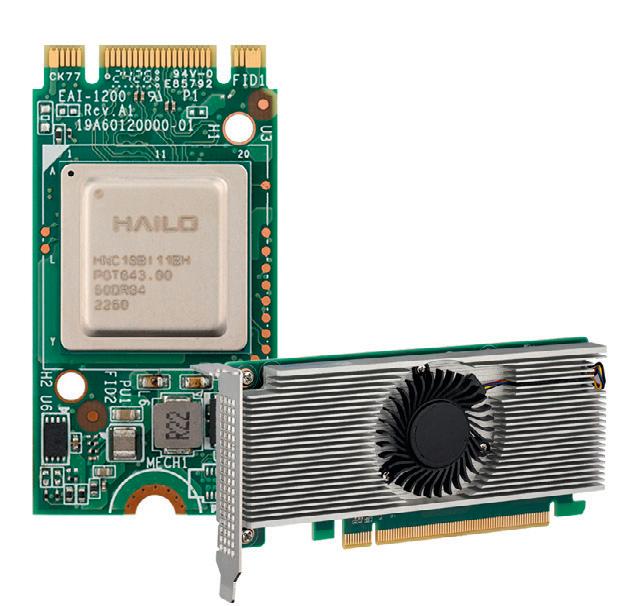
Advantech has launched the EAI-1200 and EAI-3300 AI acceleration modules, powered by Hailo-8 AI processors. Delivering up to 52 TOPS with over 12 times the power efficiency of comparable AI modules and GPUs, the modules come in standard M.2 and PCIe form factors. They can be integrated with x86 and ARM-based platforms, thereby enabling quick AI upgrades for existing systems. By offloading inference tasks to the Hailo-8 NPU while managing application processing on the CPU, the modules also enhance resource efficiency. A user-friendly software suite — including Edge AI SDK, Dataflow Compiler and TAPPAS — streamlines AI deployment and development.
The EAI-1200 M.2 AI module, powered by a single Hailo-8 VPU, delivers up to 26 TOPS while consuming just 5 W. Designed for integration, it operates in temperatures from -40 to 65°C with an optional heatsink. Suitable for applications like baggage screening, workforce safety and autonomous mobile robots (AMR), it pairs with Advantech systems such as ARK-1221L, AIR-150 and AFE-R770.
Featuring dual Hailo-8 VPUs, the EAI-3300 PCIe AI card provides 52 TOPS of AI processing at just 15 W. Its low-profile design and efficient cooling enable operation from -40 to 70°C. Compatible with AIR-510, AIMB-279 and ARK-3534D, it is designed for medical imaging, traffic monitoring and defect inspection.
Advantech Australia Pty Ltd www.advantech.net.au
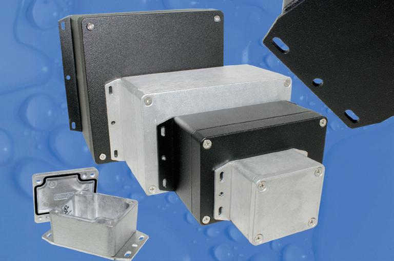
ALUMINIUM ENCLOSURE
Hammond has introduced the IP68 1550ZF range, flanged versions of all 18 sizes in the established 1550Z rugged thick wall heavy-duty diecast enclosure family. The full-size flange is spot-welded to the base to provide a strong and smooth mounting plate for use when the units are secured to a surface.
The 18 sizes range from 50 x 45 x 30 mm to 223 x 147 x 83 mm, with the lids’ thickness ranging from 5–33 mm in depth depending on the size. The tongue and groove design and a pre-formed one-piece silicone rubber gasket gives the IP68 environmental protection so the enclosures are suitable for installation in environments where dust and water will be present.
They are UL and cUL Listed and have been independently tested to IP66, IP67 and IP68; they are also rated to NEMA Type 4, 4X, 12 and 13. All sizes except the smallest have an impact rating of IK08, defined in IEC 62262 as the equivalent to the impact of a 1.7 kg mass dropped from 300 mm above the impacted surface.
They are available in a natural finish or with a tough polyester black powder finish to both the outside and inside of the enclosure.
Hammond Electronics Pty Ltd
www.hammfg.com
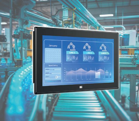
15.6″ FANLESS PANEL PC
ICP Electronics Australia has introduced iEi’s PPC2-CW156A-ADLP 15.6 ″ fanless panel PC.
The fanless industrial panel PC is designed for demanding environments and powered by Intel Alder Lake-P and Raptor Lake-P processors. It offers good performance and versatility, supporting 12th and 13th Gen Intel Core i7/i5/i3 mobile processors, with 8 GB of DDR4 SO-DIMM memory (expandable to 64 GB).
The 15.6 ″ full HD display features a 10-point capacitive touchscreen with anti-glare and anti-UV coating, enabling clear visibility even in challenging light conditions. The device also supports 4K UHD output via HDMI, making it suitable for highresolution visual applications.
For connectivity, the panel PC is equipped with dual 2.5 GbE LAN ports, four USB 3.2 Gen1 ports, and multiple M.2 expansion slots, allowing for extensive peripheral integration. Remote management is enabled with optional IPMI 2.0 support, facilitating system monitoring and maintenance from afar.
Built with a durable aluminium and SECC enclosure, the panel PC is IP65-compliant, ensuring protec tion against dust and water. Additionally, its fanless design allows for operation in harsh environments, withstanding temperatures ranging from -20 to 60°C, making it suitable for industrial applications.
ICP Electronics Australia www.icp-australia.com.au
FANLESS INDUSTRIAL COMPUTER
The Tensor i22 Fanless Industrial Computer is a rugged, high-performance system designed for industrial and edge computing applications.
Built with reliability in mind, it features a fanless design for silent operation and resistance to dust and debris, making it suitable for harsh environments.
Equipped with Intel 12th Gen Alder Lake processors, the computer can provide robust computing power and energy efficiency for demanding tasks such as industrial automation, machine vision and IoT edge deployments.
The compact system supports dual 2.5GbE LAN ports for high-speed network connectivity, multiple USB and serial ports for peripheral integration, and optional expansion slots for custom configurations. It also offers wide operating temperature ranges and is tested for shock and vibration resistance to enable good performance in challenging conditions.
It supports advanced storage solutions, including NVMe SSDs, providing rapid data access and secure storage for critical applications. With its compact form factor and versatile mounting options, it integrates seamlessly into industrial set-ups, vehicles or control cabinets.
Metromatics provides local sales, service and support for the Tensor i22 to help Australian users with expert assistance and ongoing support for their industrial computing needs.
Metromatics Pty Ltd www.metromatics.com.au
How AI is remodelling the IoT
Back in 1956, Allen Newell, Cliff Shaw and Herbert Simon put together a computer program called The Logic Theorist. Funded by the RAND Corporation, the program intended to mimic the problem-solving skills of a human and is considered by many to be the first example of artificial intelligence (AI).
Fast forward to today, and the poster child for AI is the large language model (LLM). LLMs are computational algorithms that achieve general-purpose language generation and other natural language processing tasks by learning statistical relationships from text documents during an intensive training process. OpenAI’s ChatGPT is perhaps the best-known example.
Useful though they are, for the IoT it is not the potential of LLMs that’s driving things forward. Where things get exciting is when huge volumes of data collected by automated systems are used to train machine learning (ML) algorithms that are later deployed to make IoT devices make better and smarter decisions. ML is an application of AI that involves training algorithms on large datasets, enabling computers to make predictions or decisions based on patterns and insights derived from the data, without being explicitly programmed to perform specific tasks. This process enhances the capabilities and intelligence of machines over time as they process more data.
The IoT can be described as a global interconnected network with the capacity to collect a virtually limitless volume of data. That data can be fed to computers in the cloud and used to fuel ML algorithms that enhance the intelligence of the billions of connected devices making up the network. Even the most modest IoT device can become continually smarter, offering huge potential for the future of industry, commerce, education, medicine and more. iStock.com/Userba011d64_201
RESEARCHERS CREATE
QUANTUM ‘SCHRÖDINGER’S CAT’ IN SILICON CHIP
A team led by UNSW quantum engineers has created a ‘Schrödinger’s cat’ — a famous quantum thought experiment — inside a silicon chip.
UNSW engineers have demonstrated a well-known quantum thought experiment in the real world. Their findings deliver a new and more robust way to perform quantum computations — and they have important implications for error correction, one of the biggest obstacles standing between them and a working quantum computer.
Quantum mechanics has puzzled scientists and philosophers for more than a century. One of the most famous quantum thought experiments is that of the “Schrödinger’s cat” — a cat whose life or death depends on the decay of a radioactive atom.
According to quantum mechanics, unless the atom is directly observed, it must be considered to be in a superposition — that
is, being in multiple states at the same time — of decayed and not decayed. This leads to the troubling conclusion that the cat is in a superposition of dead and alive.
“No one has ever seen an actual cat in a state of being both dead and alive at the same time, but people use the Schrödinger’s cat metaphor to describe a superposition of quantum states that differ by a large amount,” said UNSW Professor Andrea Morello, leader of the team that conducted the research, published recently in the journal Nature Physics
Atomic cat
For this research paper, Professor Morello’s team used an atom of antimony, which is much more complex than standard ‘qubits’, or quantum building blocks.
“In our work, the ‘cat’ is an atom of antimony,” said Xi Yu, lead author of the paper.
“Antimony is a heavy atom, which possesses a large nuclear spin, meaning a large magnetic dipole. The spin of antimony can take eight different directions, instead of just two. This may not seem much, but in fact it completely changes the behaviour of the system. A superposition of the antimony spin pointing in opposite directions is not just a superposition of ‘up’ and ‘down’, because there are multiple quantum states separating the two branches of the superposition.”
This has profound consequences for scientists working on building a quantum computer using the nuclear spin of an atom as the basic building block.
“Normally, people use a quantum bit, or ‘qubit’ — an object described by only two quantum states — as the basic unit of quantum information,” said co-author Benjamin Wilhelm.
“If the qubit is a spin, we can call ‘spin down’ the ‘0’ state, and ‘spin up’ the ‘1’ state. But if the direction of the spin suddenly changes, we have immediately a logical error: 0 turns to 1 or vice versa, in just one go. This is why quantum information is so fragile.”
But in the antimony atom that has eight different spin directions, if the ‘0’ is encoded as a ‘dead cat’, and the ‘1’ as an ‘alive cat’, a single error is not enough to scramble the quantum code.
“As the proverb goes, a cat has nine lives. One little scratch is not enough to kill it. Our metaphorical ‘cat’ has seven lives: it would take seven consecutive errors to turn the ‘0’ into a ‘1’! This is the sense in which the superposition of antimony spin states in opposite directions is ‘macroscopic’ — because it’s happening on a larger scale, and realises a Schrödinger cat,” said Yu.
Scalable technology
The antimony cat is embedded inside a silicon quantum chip, similar to the ones we have in our computers and mobile phones, but adapted to give access to the
quantum state of a single atom. The chip was fabricated by UNSW’s Dr Danielle Holmes, while the atom of antimony was inserted in the chip by colleagues at the University of Melbourne.
“By hosting the atomic ‘Schrödinger cat’ inside a silicon chip, we gain an exquisite control over its quantum state — or, if you wish, over its life and death,” said Holmes.
“Moreover, hosting the ‘cat’ in silicon means that, in the long term, this technology can be scaled up using similar methods as those we already adopt to build the computer chips we have today.”
The significance of this breakthrough is that it opens the door to a new way to perform quantum computations. The information is still encoded in binary code, ‘0’ or ‘1’, but there is more ‘room for error’ between the logical codes.
“A single, or even a few errors, do not immediately scramble the information,” said Morello.
“If an error occurs, we detect it straight away, and we can correct it before further errors accumulate. To continue the
‘Schrödinger cat’ metaphor, it’s as if we saw our cat coming home with a big scratch on his face. He’s far from dead, but we know that he got into a fight; we can go and find who caused the fight, before it happens again and our cat gets further injuries.”
The demonstration of quantum error detection and correction — a ‘Holy Grail’ in quantum computing — is the next milestone that the team will address.
The work was the result of a vast international collaboration. Several authors from UNSW Sydney, plus colleagues at the University of Melbourne, fabricated and operated the quantum devices. Theory collaborators in the USA, at Sandia National Laboratories and NASA Ames, and Canada, at the University of Calgary, provided precious ideas on how to create the cat, and how to assess its complicated quantum state.
“This work is a wonderful example of open-borders collaboration between worldleading teams with complementary expertise,” said Morello.
This is a modified version of a news item published by UNSW Sydney.
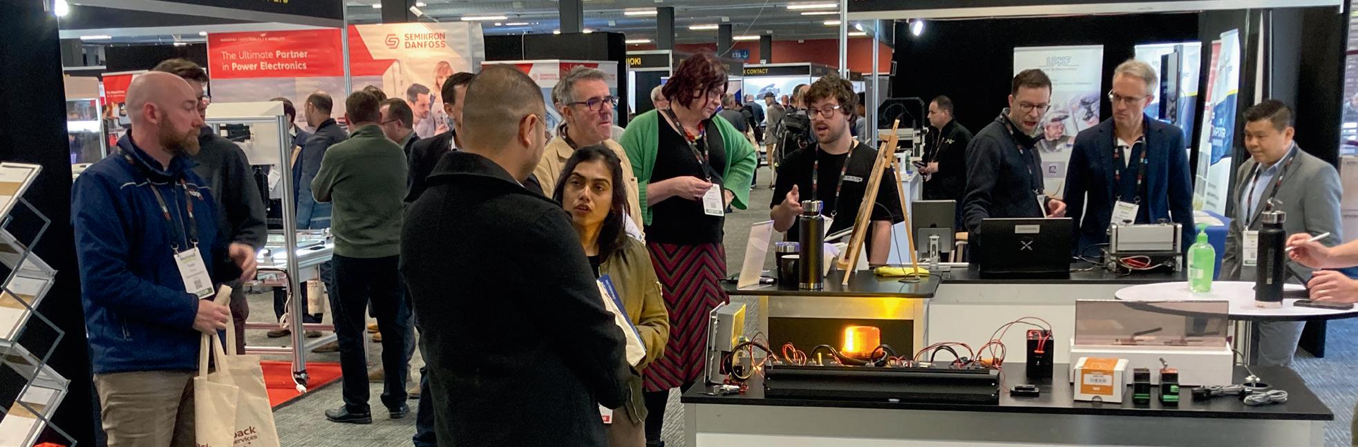
ELECTRONICS EXPO RETURNS TO MELBOURNE AUSTRALIA’S LARGEST
Electronex — The Electronics Design and Assembly Expo & Conference — will be held in the Melbourne Convention and Exhibition Centre from 7–8 May 2025.
Electronex is Australia’s major exhibition for companies using electronics in design, assembly, manufacture and service in Australia.
Electronex will be co-located with Australian Manufacturing Week, with trade visitors able to attend both events on the Wednesday and Thursday. Noel Gray, Managing Director of Electronex and Organiser AEE, said, “Following the success of the co-location in 2023 we are delighted to again be holding Electronex alongside Australia’s premier manufacturing event. Hundreds of exhibitors will be meeting face to face with thousands of trade visitors, creating the largest event for the manufacturing sector in Australia. Electronex focuses on the hi-tech end of manufacturing and visitors will be able to see the entire spectrum of the latest products, technology and turnkey solutions for the electronics and manufacturing industries at the one venue.”
Electronex features a wide of range of electronic components, surface mount and inspection equipment, test and measurement and other ancillary products and services. Companies can also discuss their specific requirements with contract manufacturers that can design and produce turnkey solutions
for their products. Many companies will be launching and demonstrating new products and technology at the event and over 100 local and international companies will be represented at this year’s Expo, making it the largest ever held. The show attracts designers, engineers, managers and other decision-makers who are involved in designing or manufacturing products that utilise electronics and is the only specialised event for the electronics industry in Australia. With many Australian manufacturers now focusing on niche products and hi-tech applications, the event provides an important focal point for the industry in Australia.
Free seminars and competitions
A series of free seminars will also be held on the show floor with visitors able to attend on the day with no pre-booking required. These sessions will provide an overview of some of the hot topics and key issues for the industry. Topics include: Reliability in Programmable Power Supplies, Affordable Yet Versatile Multifunction 12 in 1 Test & Measurement Devices, Successful Product Development, Handling Complexity in PCB Manufacturing and Assembly, Compliance and
Regulatory Approval to Sell Your Products in AU & Globally, Microchip’s AI-Centric 64-Bit Processors, Smart AI In Conformal Coating and Dispensing, Software-defined Test: A More Efficient Way to Automate and Validate, High Mix SMT Manufacturing, Leveraging Strategic Partnerships to Transform Traditional Products into Smart Innovations, Advancing Edge Computing with AMD, Technology & Process Capabilities for SMT PCB Assembly in Australia, and Building a Product Test System the Right Way. Visit the show website for times and session details.
Competitions will also be held on the show floor where visitors can test their skills against their peers. Could you be Australia’s champion wire harness assembler or hand soldering expert? The SMCBA, with the support of IPC International, will once again be conducting the Australian Round of the IPC Hand Soldering Competition (HSC) and — excitingly — the Australian Round of the inaugural IPC/WHMA Wire Harness Competition (WHC)!
The WHC will be a timed event where entrants assemble a multi-wire harness with various connectors and termination types! The winner will have the opportunity to compete in the international finals at the iEMi Expo, Bengaluru India, January 2026! Free Expo registration: www.electronex.com.au
Australasian Exhibitions and Events Pty Ltd www.electronex.com.au
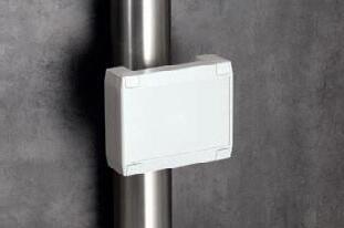
ENCLOSURES FOR MOUNTING ARM SYSTEMS
OKW Gehäusesysteme offers a range of advanced enclosures for mounting arm and suspension systems. These systems enable flexible positioning of medical devices and monitors, making them vital in operating theatres and intensive care units.
The Carrytec enclosure features a functional handle and large surfaces suitable for user interfaces (small = 8.4 ″, medium = 10.4 ″, large = 13.4 ″). It enables users to align and position displays and operating surfaces, with clean cable routing.
The slightly smaller Interface-terminal is a multifunctional electronics enclosure with numerous design options, a range of accessories and optional IP54 protection.
ROLEC OKW Australia New Zealand P/L www.okw.com.au 7–8
For added robustness, the Smart-terminal aluminium profile enclosure, with its recessed control panel for installing and protecting displays, membrane keypads and control elements, is also a suitable choice to support medical devices.
The choice of appropriate enclosure depends on the specific application requirements and spatial conditions.
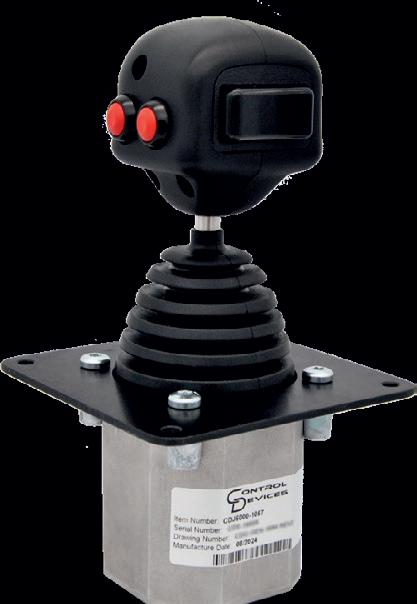
SMART AND SAFE CONTROL SOLUTIONS FOR MOBILE MACHINERY
In the rapidly evolving landscape of mobile machinery, the demand for efficient, safe, and adaptable control systems is paramount. HYDAC’s MATCH software platform emerges as a comprehensive solution, addressing these needs with precision and reliability.
What is MATCH?
MATCH is a TÜV-certified software suite designed for the development and maintenance of control software in mobile machinery. It offers optimally coordinated solutions throughout the machine’s entire life cycle, ensuring both innovation and safety are at the forefront.
Key Features and Benefits
1. Rapid Development and Redesign With MATCH, engineers can swiftly design new applications for complex vehicle or machine controls. It also facilitates quick redesigns of existing machines, components, and functions, leading to time savings of up to 50%.
2. Functional Safety Standards
Safety is integral to MATCH. The suit of tools is designed for functional safety from the outset, with all tools, libraries, and components being TÜV-certified. This ensures that control systems are future-proof and compliant with stringent safety standards.
3. Comprehensive Toolchain
MATCH’s toolchain comprises the Project Definition Tool (PDT), Test and
Simulation Environment (TSE), and Machine Service Tool (MST). These tools work seamlessly together, supporting development according to the V-model. This integrated approach enhances efficiency and traceability across all stages of development.
4. Hardware Independence and Robustness
The platform offers hardwareindependent programming, MATCH abstracts programming away from the hardware layer, allowing for flexibility in hardware selection. Its robust middleware and extensively tested and safety certified library function blocks ensure reliability and ease of portability to other hardware systems.
5. Multi-Controller Capability
MATCH supports application development at the machine level, enabling the seamless integration of multiple control units and displays. This multi-controller approach ensures cohesive functionality and communication across the entire system.
Applications Across the Machine’s Life Cycle
MATCH is designed to support various stages of a machine’s life cycle:
• System Definition & Embedded Software Engineering : From requirements management to software design and programming, MATCH
provides a structured approach to developing control systems.
• Software Test & Machine Validation: MATCH facilitates testing through all steps of the V-model, including module and integration tests, system tests, and vehicle validation. Integrated modules support a plug-and-play test environment.
• Production & End-of-Line Support : The platform streamlines end-of-line commissioning, software downloads, machine configuration, and final validation, ensuring a smooth transition from production to deployment.
• Service Organisation & Field Service Engineering : MATCH provides comprehensive tools for service and maintenance, including user-related access rights, and machine-specific diagnostic pages.
Conclusion
HYDAC’s MATCH software platform stands as a pivotal advancement in mobile machinery automation. By integrating safety, efficiency, and flexibility, it empowers engineers and developers to meet the evolving demands of the industry, ensuring that machinery is both innovative and reliable throughout its life cycle.
To learn more about MATCH software, click here.
HYDAC International
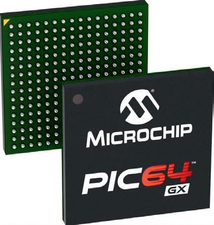
MICROPROCESSOR UNITS
The 64-bit PIC64 series of MPUs from Microchip Technology offers a range of robust solutions for various markets, from commercial to space applications.
The PIC64-GX MPUs feature a 64-bit RISC-V quad-core processor with asymmetric multiprocessing (AMP), capable of running Linux, real-time OS and bare-metal in a single processor cluster. This makes it suitable for mid-range intelligent edge computing needs.
The series of microprocessing units also features an Athena F5200 TeraFire Crypto Processor; Cryptography Research Incorporated (CRI)-patented differential power analysis (DPA) protection; integrated dual physically unclonable function (PUF), 56 kilobytes of non-volatile memory; built-in tamper detectors; and digest integrity check for sNVM and eNVM. The microprocessor units are designed to serve industrial, automotive, communications, IoT, aerospace and defence segments, making them versatile for various high-demand applications.
The series also supports a range of operating systems, build systems and drivers/middleware. It is also backed by both open-source and commercial tools.
Microchip Technology Hong Kong Limited www.microchip.com
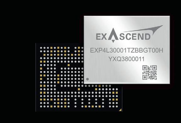
SOLID-STATE DRIVE
Control Synergy www.controlsynergy.com.au STAND A12
The Exascend AS500 BGA solid-state drive (SSD) is designed to power the future of automotive innovation, delivering high-speed and compact storage for connected vehicles, ADAS, infotainment systems and autonomous driving applications. With a PCIe 3.0 NVMe 1.3 interface, the product facilitates fast data transfer, minimal latency and enhanced responsiveness, making it suitable for real-time, mission-critical automotive workloads.
Built with automotive-grade 3D TLC NAND, the SSD features wide temperature tolerance (-40 to 105°C) and rugged durability to withstand a range of environmental conditions. Advanced error correction, power loss protection and intelligent thermal management enable data integrity under continuous operation. With its ultra-compact BGA form factor, the SSD can be integrated into space-constrained automotive designs while supporting storage capacities up to 1 TB. Whether for high-definition navigation, real-time sensor fusion or AI-powered vehicle systems, the product enables fast performance and the endurance needed for next-generation automotive applications.
OPTICAL MEMORY UNIT
BOOSTS PROCESSING SPEED
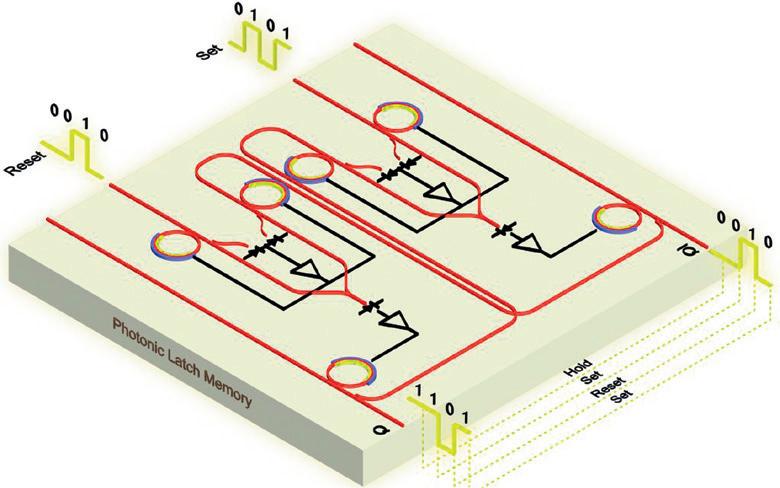
Researchers have developed a new type of optical memory called a programmable photonic latch that is fast and scalable. This fundamental memory unit enables temporary data storage in optical processing systems, offering a high-speed solution for volatile memory using silicon photonics.
The new integrated photonic latch is modelled after a set-reset latch, a basic memory device used in electronic devices to store a single bit by switching between set (1) and reset (0) states based on inputs.
“While optical communications and computing have seen significant progress over the past decades, data storage has been predominantly implemented using electronic memory,” said the study’s author Farshid Ashtiani from Nokia Bell Labs. “Having a fast optical memory that can be used with optical processing systems, as well as other optical systems used in communications or sensing, would make them more efficient in terms of energy and throughput.”
In the Optica Publishing Group journal Optics Express , the researchers describe a proof-of-concept experiment in which they demonstrated the photonic latch using a programmable silicon photonic platform. Features such as optical set and reset, complementary outputs, scalability and compatibility with wavelength division multiplexing (WDM) make this approach promising for faster and more efficient optical processing systems.
“Large language models like ChatGPT rely on massive amounts of simple mathematical operations, such as multiplication and addition, performed iteratively to learn and generate answers,” Ashtiani said. “Our
memory technology could store and retrieve data for such systems at high speeds, enabling much faster operations. While a commercial optical computer is still a distant goal, our high-speed optical memory technology is a step toward this future.”
Advancing integrated optical memory
Optical technologies have been instrumental in advancing communication systems, from long-haul data transmission and data centre connectivity to emerging technologies like optical interconnects and computing. However, data storage remains predominantly electronic due to its scalability, compactness and costeffectiveness. This presents challenges for optical processing systems because transferring optical data to electronic memory — and
This new type of optical memory unit, called a programmable photonic latch, is fast and scalable. It could offer a high-speed silicon photonics solution for volatile memory.
back — increases energy consumption and introduces latency.
Although there has been extensive research in the area of optical memory, most implementations rely on bulky, costly and energyintensive setups or specialised materials that are not typically offered in commercially available silicon photonic processes, leading to higher costs and lower yields.
To overcome these challenges, the researchers created an integrated programmable photonic latch based on optical universal logic gates using silicon photonic micro-ring modulators. These devices can be implemented in commercially available silicon photonic chip fabrication processes. They combined two optical universal logic gates to create an optical latch that can hold optical data.
Farshid Ashtiani, Nokia Bell Labs.
Creating memory that is scalable and fast
Ashtiani says that one key advantage of the new system is its scalability. “Because each memory unit has an independent input light source, it is possible to have several memory units working independently without affecting each other through optical power loss propagation,” he said. “The memory units can also be co-designed with the existing silicon photonic systems and be built reliably and with very high yields.”
Another advantage is the photonic memory unit’s wavelength selectivity, which allows it to work seamlessly with WDM. This is because the unit’s microring modulators are designed to operate at specific wavelengths, enabling multi-bit data storage within a single memory unit. Additionally, it enables fast memory response time, measured in tens of picoseconds, outpacing the clock speeds of advanced digital systems and supporting high-speed optical data storage.
To demonstrate this approach to optical memory before making dedicated chips, the researchers used a programmable photonic platform to implement the universal logic gates and the optical latch through experiments and realistic simulations.
The researchers tested the gates under different input scenarios. Even in the presence of random variations, the gates reliably generated the desired outputs. Similarly, the latch also performed all functions — set, reset and hold— accurately in the presence of input power variations.
Next, the researchers would like to pursue several research directions to make the new memory units more practical. This includes scaling the technology to a larger number of memory units and fabricating dedicated photonic memory chips. This, combined with the WDM compatibility, would enable higher on-chip photonic memory density. They would also like to develop a way to use a single manufacturing process to integrate both the photonic memory circuit and the electronics needed to control it.
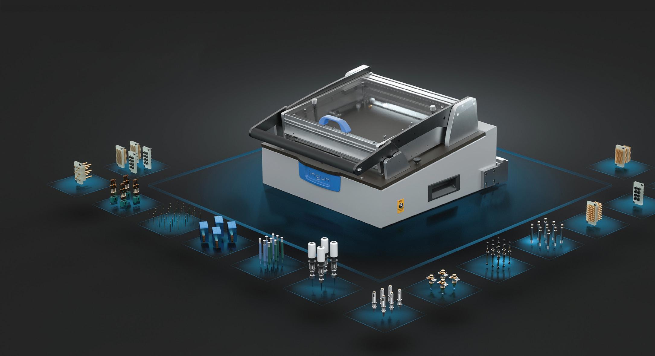
MICRO DISPENSING SYSTEM
The BDTronic Mini Dis is a micro dispensing device designed for high-precision fluid applications. Engineered to meet the demands of modern manufacturing, it offers control down to the nanolitre range for dispensing adhesives, sealants and conductive materials, making it suitable for microelectronics and medical applications.
The micro dispensing system’s modular and flexible design make it adaptable to various production environments. The system’s contactless jet dispensing enables rapid application without substrate contact. The system is also compatible with automated production lines.
Onboard Solutions www.onboardsolutions.com.au
7–8 MAY 2025
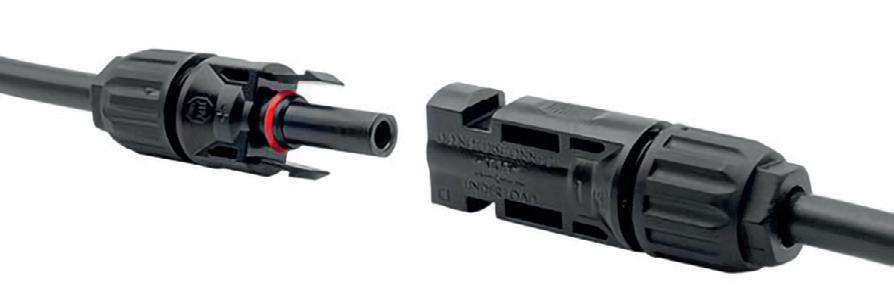
PHOTOVOLTAIC/SOLAR CONNECTOR
The Multicomp Pro MP013877 photovoltaic/solar connector is designed for use in solar power systems. The connector enables secure and efficient connections between solar panels and other components within the PV system.
Both male and female couples are included in one pack. The couplers provide a stable connection to facilitate the operation of solar power systems. The connectors are built to withstand harsh environmental conditions, making them suitable for outdoor applications. They feature high voltage and current ratings and meet compliance and flammability standards, for safe operation within PV systems. element14 au.element14.com
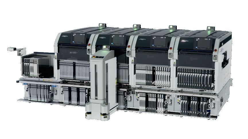
PICK AND PLACE MACHINE
The NXTR A model, part of the FUJI Smart Factory Platform, is a pick and place machine that is designed to enhance productivity, maintain high-quality standards and reduce the need for manual intervention, thereby streamlining the production process.
The pick and place machine is an automated part supply and exchange system. This system is enabled by the Smart Loader, which automates part supply and changeover for the next production according to the production schedule. In a line equipped for automatic part supply, the Smart Loader automatically supplies machines with cassette-type feeders from a buffer station within the line. This allows for the necessary parts to be set in the buffer station in advance, thereby enhancing the efficiency of the production process. This system eliminates short stops due to part supply errors, but also mitigates issues caused by delays and mistakes during supply work.
Another key feature of the pick and place machine is its ability to handle a range of panel sizes. The model supports panels up to 750 x 610 mm on single-lane conveyors and up to 370 x 280 mm on dual-lane conveyors. This expanded conveyable panel size allows the NXTR A model to support a greater variety of production, from large panel production to the efficient production of double-sided, small to medium-sized panels.
The pick and place machine’s automated part supply and exchange system, automatic feeders and ability to handle a range of panel sizes make it a versatile and efficient solution for any production line. With its focus on maintaining high-quality placements and reducing manual intervention, the NXTR A model is suitable for a range of smart factories.
Kobot Systems smt.fuji.co.jp/en
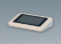
SOLID-BOX ADVANCED ENCLOSURES
In the realm of medical technology, suspension systems offer a multitude of applications, enabling flexible positioning of medical devices and monitors. These systems are necessary for patient monitoring, tracking vital functions such as heart rate, blood pressure and oxygen saturation.
Additionally, they are indispensable in operating theatres and intensive care units, where the ability to adjust equipment flexibly is needed for high-precision work. Even the less critical applications, such as patient information displays, should not be overlooked.
OKW Gehäusesysteme offers a variety of suitable models in its product range.
The CARRYTEC enclosure, for instance, features a functional handle and large surfaces suitable for user interfaces (S: 8.4 ″/21 cm; M: 10.4 ″/26 cm; L: 13.4 ″/34 cm), making it suitable for aligning and positioning displays and operating surfaces, as well as enabling clean cable routing.
The smaller INTERFACE-TERMINAL is a multifunctional electronics enclosure with numerous design options, a range of accessories and optional IP54 protection.
The SMART-TERMINAL aluminium profile enclosure, with its recessed control panel for installing and protecting displays, membrane keypads and control elements, is also a suitable choice for added robustness.
The selection of the appropriate enclosure depends on the specific application requirements and spatial conditions.
ROLEC OKW Australia New Zealand P/L www.okw.com.au
AI ACCELERATION MODULES
Advantech has introduced the EAI-1200 and EAI-3300 AI acceleration modules, powered by Hailo-8 AI processors. Delivering up to 52 TOPS with 12x the power efficiency of traditional AI modules, these M.2 and PCIe solutions enable AI upgrades for x86 and ARM platforms. Developers can run inference on the Hailo-8 NPU while offloading application processing to the CPU, thereby optimising system performance.
Paired with user-friendly software toolkits — including the Edge AI SDK, Dataflow Compiler and TAPPAS — these modules streamline edge AI development for vision applications.
The EAI-1200 features a single Hailo-8 VPU, delivering up to 26 TOPS while consuming just 5 W. Its compact M.2 form factor enables easy integration, with an optional heatsink supporting operation from -40 to 65°C. Designed for security and automation, it also enhances AI applications such as baggage screening, workforce safety and autonomous mobile robots (AMR). The module is also compatible with Advantech systems including ARK-1221L, AIR-150 and AFE-R770.
Equipped with dual Hailo-8 VPUs, the EAI-3300 delivers 52 TOPS at up to 15 W. Its low-profile PCIe design enables easy deployment across various chassis, with an optimised cooling system for operation between -40 and 70°C. Supporting medical imaging, traffic monitoring and defect inspection, it integrates with AIR-510, AIMB-279 and ARK-3534D.
Advantech Australia Pty Ltd www.advantech.net.au
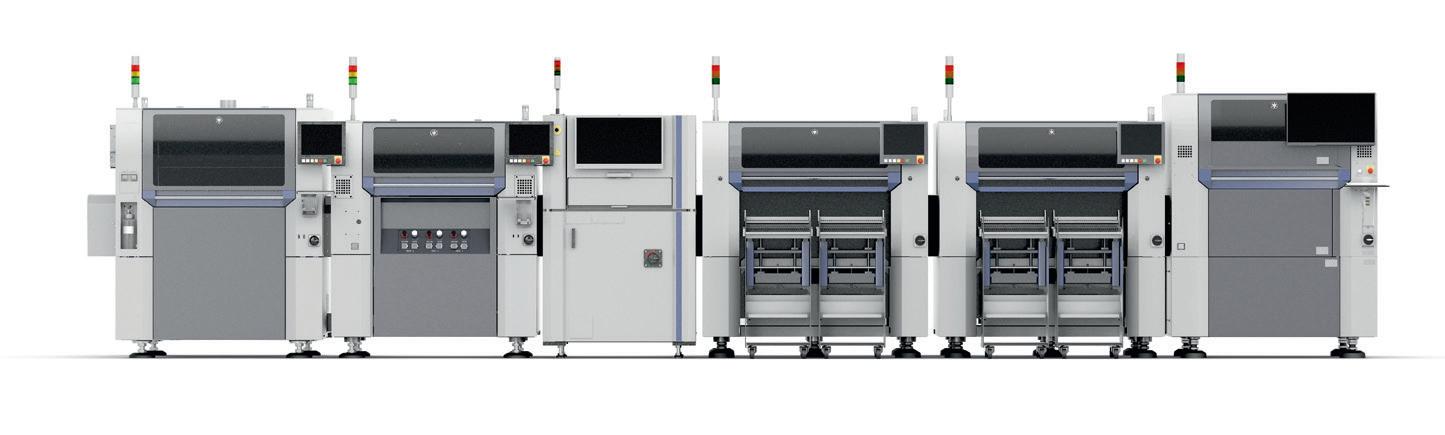
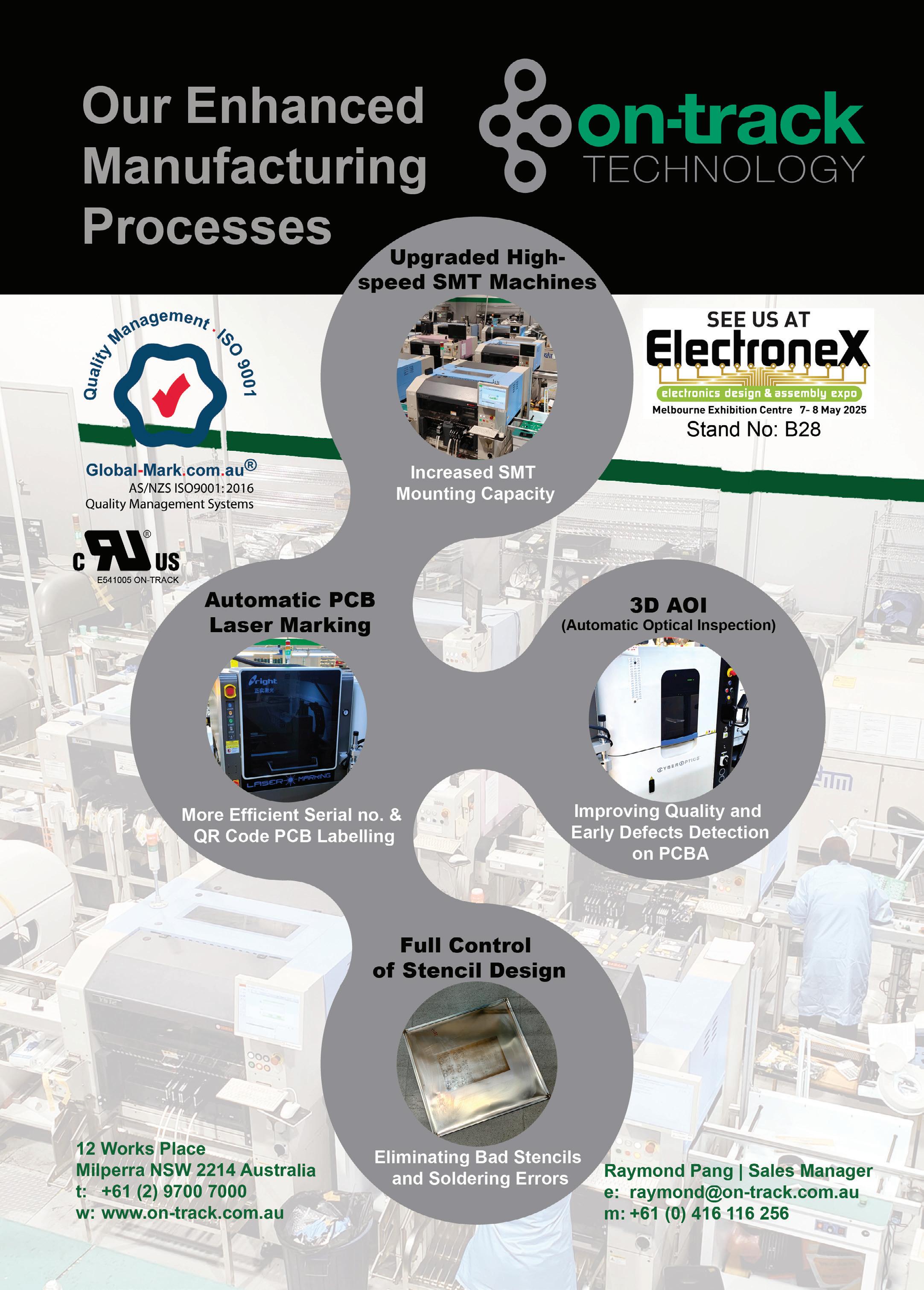
SURFACE-MOUNTER HARDWARE
Yamaha Robotics SMT Section has launched the 1-Stop Smart Solution, designed to enhance the performance of its highspeed pick and place machines. These innovations target industries with stringent quality demands such as automotive, aerospace and medicine.
The key hardware-based enhancements for Yamaha Mounters include nozzle-tip force measurement to enable the early detection of issues like blockages. This allows for timely nozzle maintenance, for enhanced end-of-line production yield. The system also tracks changes in force and measures component-placement force to within 0.1N resolution.
LCR verification measures the inductance, capacitance or resistance value of components in SMD-chip packages to verify the correct part type and tolerance before placement. This helps users detect issues like feeder errors, reel errors or defective components before placement to maximise first-pass yield and avoid rework. The LCR unit can be fitted to Yamaha YRM mounters and legacy YSM machines without special modifications.
A large board option enables YRM mounters to handle boards up to 1.5 m long and 510 mm wide, suitable for assemblies like extralarge LED-lighting boards. This option increases the maximum board size by more than 30% compared to standard YRM mounters and accepts boards up to 10 mm thick and weighing up to 10 kg. It allows manufacturers to work with assemblies designed for high thermal capacity, such as heavy-gauge copper or aluminium-insulated metal substrates (IMS).
These options can be implemented individually or together to boost surface-mount production performance and extend the advantages of the 1-Stop Smart Solution, which comprises Yamaha’s YRP printers, YRM-D dispensers, YRM mounters and YRi-V inspection systems. The 1-Stop Smart Solution allows users to configure a complete SMT assembly line from Yamaha, unified with a common software platform and smart tools that facilitate flexibility, quality and productivity.
Hawker Richardson is the exclusive supplier of Yamaha SMT line products in Australasia, providing regional access to Yamaha’s advanced PCB assembly solutions.
Hawker Richardson www.hawkerrichardson.com.au
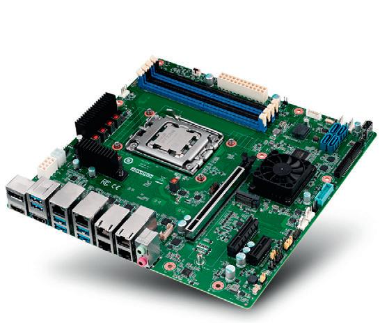
COMPUTER-ON-MODULES
congatec has launched the COM Express Compact Computer-on-Modules with AMD Ryzen Embedded 8000 Series processors. The modules are based on the computing cores of the Ryzen processors featuring up to eight ‘Zen 4’ cores, innovative XDNA NPU and Radeon RDNA 3 graphics.
This makes the conga-TCR8 Type 6 modules suitable for high-volume applications requiring a combination of advanced AI, graphics and computing power. OEMs in medical imaging, test & measurement, AI-supported POS/POI systems and professional gaming can also leverage these long-term available COM Express Compact modules to accelerate innovation. With a broad, scalable TDP range of 15–54 W, these modules are also suitable for upgrading existing designs.
The conga-TCR8 computer-on-modules support up to 128 GB DDR5-5600 memory with error correction code (ECC) for data-intensive and data-critical applications. With the integrated AMD XDNA NPU (16 TOPS) and AMD Radeon RDNA 3 graphics, the modules deliver a combined computing power of up to 39 TOPS. They also support immersive graphics output on up to four displays with resolutions as high as 8K. For fast peripheral connectivity, they offer six PCIe Gen 4 (8 lanes) with PEG x8 Gen 4, three DisplayPort (DP) interfaces, one eDP or LVDS, four USB 3.2 Gen 2 ports, and four USB 2.0 ports.
The modules are also available as application-ready aReady.COMs, with custom pre-installed and validated operating systems like ctrlX OS, Ubuntu and/or RT Linux, optional system consolidation via aReady.VT, and IoT connectivity via aReady.IOT. On request, the modules can be pre-installed with the customer’s application, allowing for simple plug-and-play integration into the finished system. Congatec Australia Pty Ltd www.congatec.com
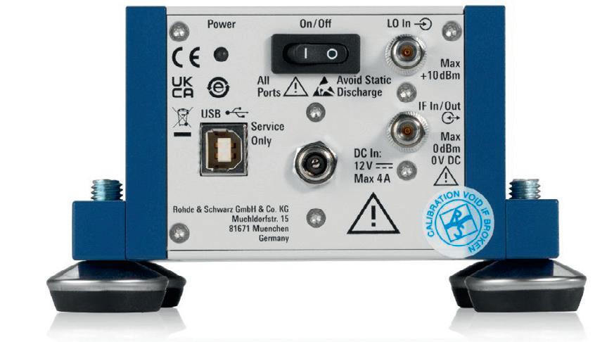
FREQUENCY CONVERTER
The Rohde & Schwarz FC330ST frequency converter is designed for up- and downconversion of intermediate frequency (IF) signals to and from the RF frequency range from 220–330 GHz. A high-performance mixer with low conversion loss enables precise measurements, while the integrated IF amplifier enhances sensitivity and signal performance. The frequency converter supports a wide IF range up to 35 GHz, enabling the transmission and reception of ultra-wideband signals. The optional FC330-Z50 external amplifier features a low noise figure and can be used to boost transmitter output power or as a low-noise amplifier to improve the receiver sensitivity.
To complete the solution, a range of accessories is available, including a variety of bandpass filters, tuneable attenuators and horn antennas.
The frequency converter utilises a WR3.4 waveguide RF connector that meets the WR3 EIA standard to provide frequency coverage. To support flexible operation and minimise unwanted signals, a set of five external bandpass filters is available, each with a 30 GHz passband. These filters enable the selective elimination of sideband and local oscillator signals, thereby enhancing signal quality across the entire frequency range.
The IF frequency range of the FC330 from 1–35 GHz enables the transmission of wideband signals and provides a range of options to select the optimal IF/LO combination. Each frequency converter is characterised in the factory and supplied with measurement and alignment data on a USB flash drive. This flexibility in customisation enables control of the system to achieve a specific RF frequency, making it a suitable solution for various applications.
The frequency converter also incorporates an integrated IF amplifier, which serves to enhance sensitivity in receive mode and optimises the mixer input levels in transmit mode. By amplifying the downconverted IF signal directly after the mixer, the amplifier also improves overall system performance. In transmit mode, the amplifier optimises the mixer input level, resulting in improved signal quality.
The R&S FC330-Z50 external amplifier operates within the frequency range of 220–330 GHz. It can be supplied with power directly from the R&S FC330 and provides a typical gain of 15 dB, delivering signals with up to +8 dBm output power (measured at saturation). Due to its low noise figure, the amplifier is suitable for transmit (TX) as well as receive (RX) direction.
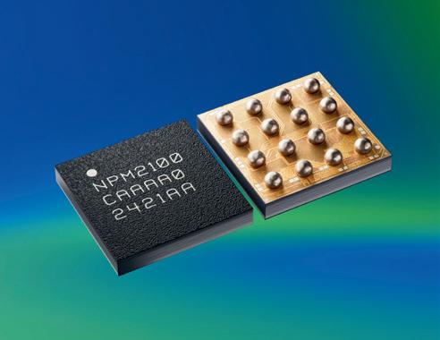
Nordic Semiconductor has launched the nPM2100 Power Management IC (PMIC), designed to prolong the operating time per battery for primary (non-rechargeable) battery applications by managing energy resources using an ultra-efficient boost regulator and a range of energy-saving features. The PMIC has a range of applications, including wireless mice and keyboards, consumer asset tracking, remote controls and body-worn medical devices.
The PMIC’s boost regulator and energy-saving features — including primary-cell fuel gauging — address power management inefficiencies while also using all of the battery’s stored energy before the cell is thrown away.
The power management IC manages the power supply for low-power systems-on-chip (SoCs) or microcontroller units (MCUs) such as Nordic’s nRF52, nRF53 and nRF54 series of advanced wireless multiprotocol products. The PMIC is optimised for maximum efficiency and compact size and is configurable through an I2C-compatible Two Wire Interface (TWI). This interface enables access to configure a range of advanced functions, including ship mode and battery fuel gauging. The PMIC also features two GPIOs that can be repurposed to direct control lines to time-critical control functions as an alternative to serial communication.
The PMIC targets primary battery applications. Examples of supported batteries are one or two AA/AAA/LRxx batteries (in series), or one 3 V LiMnO2 cell. Single- or dual-cell silver oxide and zinc-air coin-cell batteries are also supported, plus any other primary battery that operates within the nPM2100’s input voltage range.
The nPM2100 features a boost regulator with an output range of 1.8–3.3 V, powered from an input range of 0.7–3.4 V. The regulator can deliver up to 150 mA maximum current. The regulator also powers a Load Switch/ LDO supplying up to 50 mA across an output range of 0.8–3.0 V. The regulator also features a quiescent current (IQ) of 150 nA.
Nordic Semiconductor www.nordicsemi.com
BENCHTOP IONISER
STAINLESS STEEL PUSH-BUTTONS
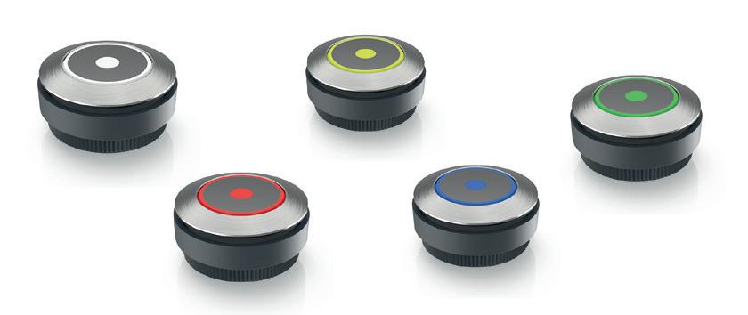
RAFI’s RAFIX 30 FS+ series of control devices includes illuminated push-buttons in a modern stainless steel design with ring and spot illumination. With an installation height of 3.45 mm, the flat actuators have a stainless steel front ring and a push-button surface with a metal V2A inlay and translucent illuminated dot. An SMT LED is integrated as the light source for the push-buttons, which are available as standard in five illuminated colours: white, red, yellow, green and blue.
The actuators offer IP65 protection on the front and, like all control and signalling devices in the series, are dimensioned for standard installation openings of 30.3 mm. They can be used in temperature ranges from -25 to +70°C and are designed to have a service life of one million actuation cycles. Due its clear tactile feedback, the push-button series is also suitable for glove operation.
The push-buttons can be combined with PCB switching elements for PCB applications as well as with QC switching elements for classic wiring. In the PCB version, the push-buttons achieve an installation depth of 15.7 mm. The QC switching elements are connected individually via 2.8 x 0.8 mm flat plugs with an installation depth of 31.9 mm. Both switching element variants are available in versions with gold contacts for a maximum of 35 V and 100 mA or with silver contacts for up to 250 V and 4 A. Short-stroke adapters enable the use of MICON 5 short-stroke push-buttons as switching elements.
Switches Plus Components Pty Ltd www.switchesplus.com.au
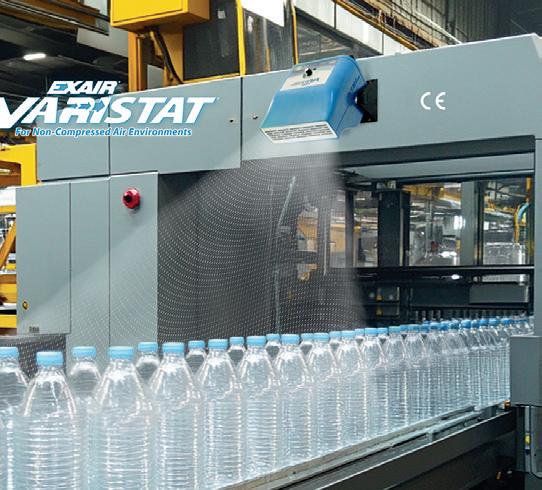
The EXAIR Varistat Benchtop Ionizer is a fan-driven static eliminator engineered to neutralise static charges on surfaces in a range of industrial environments. This ioniser is designed to provide a consistent stream of ionised airflow, eliminating static and particulates without the need for compressed air. The Varistat is now available in 230 V to meet the needs of industrial locations. Easily mounted on benchtops or machines, this static eliminator is manually adjustable and suitable for processes needing comprehensive coverage.
The 230 V model offers adjustable features, allowing for versatility. Features like selectable voltage 115 VAC/230 VAC, variable fan speed and adjustable polarity make the Varistat a comprehensive solution for eliminating static in a variety of processes and facilities. Once plugged in, the ioniser provides rapid static decay capable of reducing 1000–100 V in 0.8 seconds. This product features two replaceable ion emitter points and two 30 PPI foam filters to enhance performance over extended periods, as well as LED lights to signify proper function.
Available from Compressed Air Australia, the Varistat is part of an extensive line of static eliminating products that are UL listed and CE compliant. Products like the Intellistat Ion Air Gun, the Gen4 Super Ion Air Knife and the Gen4 Ionising Bar exhibit the range of static solutions offered and the ability to combat static in a variety of manufacturing processes.
Compressed Air Australia Pty Ltd www.caasafety.com.au
QUANTUM TELEPORTATION PERFORMED OVER BUSY INTERNET CABLES
Amanda Morris, Northwestern University
Northwestern University engineers are the first to successfully demonstrate quantum teleportation over a fibre-optic cable already carrying internet traffic.
The discovery, published in the journal Optica , introduces the new possibility of combining quantum communication with existing internet cables — greatly simplifying the infrastructure required for advanced sensing technologies or quantum computing applications.
“This is incredibly exciting because nobody thought it was possible,” said Northwestern’s Prem Kumar, who led the study. “Our work shows a path towards next-generation quantum and classical networks sharing a unified fibre-optic infrastructure. Basically, it opens the door to pushing quantum communications to the next level.”
An expert in quantum communication, Kumar is a professor of electrical and computer engineering at Northwestern’s McCormick School
of Engineering, where he directs the Center for Photonic Communication and Computing.
How it works
Only limited by the speed of light, quantum teleportation enables a new, ultra-fast, secure way to share information between distant network users, wherein direct transmission is not necessary. The process works by harnessing quantum entanglement, a technique in which two particles are linked, regardless of the distance between them. Instead of particles physically traveling to deliver information, entangled particles exchange information over great distances — without physically carrying it.
“In optical communications, all signals are converted to light,” Kumar explained.
“While conventional signals for classical communications typically comprise millions of particles of light, quantum information uses single photons.”
“By performing a destructive measurement on two photons — one carrying a quantum state and one entangled with another photon — the quantum state is transferred onto the remaining photon, which can be very far away,” said Jordan Thomas, a PhD candidate in Kumar’s laboratory and the paper’s first author. “The photon itself does not have to be sent over long distances, but its state still ends up encoded onto the distant photon. Teleportation allows the exchange of information over great distances without requiring the information itself to travel that distance.”
MOUSER ELECTRONICS: POWERING INNOVATION FOR AUSTRALIAN ENGINEERS
Over six decades ago, a high school teacher’s passion for electronics education laid the foundation for what would become Mouser Electronics — a global leader in electronic component distribution. Today, Mouser stands as a trusted partner for engineers, designers, innovators, educators, and buyers worldwide, offering cutting-edge components and resources to fuel the next generation of engineering solutions and future product development.
Fast, Reliable, and Efficient Supply Chain Solutions
Supporting Australia’s Design Engineers with the Newest Technologies
Mouser Electronics is an authorised distributor for over 1,200 leading manufacturers, offering more than 6.8 million products in stock. With a commitment to rapid product launches, Mouser introduces nearly 70,000 new components annually, ensuring that design engineers in Australia and beyond have access to 100% genuine, certified components for their latest innovations.
Mouser has built trust through consistent support and understanding of design engineers and buyers’ needs. Daphne Tien, Vice President of Marketing & Business Development for Mouser APAC, notes, “Our core value proposition has been the rapid introduction of new products and technologies, regardless of market challenges. We maintain a robust inventory of over a million different components, including a vast selection of semiconductors, connectors, sensors, passives, and more to support customers worldwide.”
With no minimum order quantity, engineers can purchase just a single part for prototyping and testing instead of having to commit to large product quantities, ensuring flexibility throughout the design process. With an extensive range of every type of component necessary to build a finished working prototype, Mouser simplifies sourcing by offering one-stop shopping. This eliminates the need for multiple suppliers. Comprehensive datasheets, application notes, and reference designs are also available to streamline workfl ows, enabling informed decisionmaking at every stage of development.
Navigating supply chain complexities is a significant challenge for engineers and procurement professionals. Mouser’s stateof-the-art global distribution centre operates with cutting-edge automation, capable of processing up to 14 orders per minute , with same-day shipping on most in-stock items. Real-time stock updates help mitigate the risk of delays and production halts due to component shortages, ensuring a steady supply for critical projects.
Mouser’s localised support enhances the customer experience by offering dedicated assistance with ordering issues, component selection, and technical inquiries. To better serve Australian customers, Mouser has opened a customer service centre in Melbourne, providing region-specific support.
Overall, by streamlining the procurement process and offering local support, Mouser helps accelerate project timelines and reduce the complexity associated with managing numerous vendor relationships.
Ensuring Quality and Design Continuity
For engineers working on high-performance applications, quality and reliability are essential. Mouser sources exclusively from the original manufacturers, implementing rigorous anti-counterfeit measures, full product traceability, and quality controls to safeguard component integrity.
To support long-term design planning, Mouser provides lifecycle management insights, including Not Recommended for New Design (NRND) labels and End-of-Life (EOL) tracking. These proactive measures help engineers and procurement teams make informed decisions and avoid supply chain disruptions.
Driving Future Innovation in Australia
As Australia continues to expand its footprint in high-tech industries such as renewable energy, and smart infrastructure, Mouser remains committed to equipping engineers with the latest resources to drive innovation. Additionally, Mouser’s website features a powerful suite of digital tools, including advanced search capabilities, an ECAD design library, and real-time inventory tracking, making it easier than ever to source and integrate the right components into designs.
Beyond distribution, Mouser also supports engineering education, providing students and academic institutions with resources that bridge the gap between theoretical learning and practical application. Through access to technical content, online tools, and the newest components, Mouser helps nurture the next generation of engineers with the knowledge needed to drive Australia’s technological progress.
Looking Ahead
Mouser remains dedicated to supporting its customers with the highest quality products and services. With a forwardlooking approach and a commitment to embracing new technologies, Mouser is poised to continue its leadership in the electronics industry for many years to come.
As the company looks to the future, it remains excited about the endless possibilities and new opportunities ahead.
Mouser Electronics au.mouser.com
SODIUM-ION STUDY SAYS
TECH NEEDS BREAKTHROUGHS TO COMPETE
A thorough analysis of market and supply chain outcomes for sodium-ion batteries and their lithium-ion competitors is the first by STEER, a new Stanford and SLAC energy technology analysis program.
Legions of battery engineers and their supporters have sought for years to build batteries cheaper than the dominant lithium-ion technology, hoping to capture some of lithium-ion’s $50 billion-a-year and growing market. The latest darling contender among researchers, startups, and venture capitalists — sodium-ion batteries — has received much attention after COVID-induced mineral supply chain challenges sent lithium prices on a wild ride. Still, achieving a low-cost contender may be several years away for sodium-ion batteries and will require technological advances and favourable market conditions, according to a new study in Nature Energy.
Sodium-ion batteries are often assumed to have lower costs and more resilient supply chains compared to lithium-ion batteries.
Despite much potential, sodium-ion batteries still face an uphill struggle. The amount of energy they hold per pound tends to be lower than lithium-ion batteries. So, possible lower materials prices aside, the cost per unit of energy stored remains higher for sodium-ion batteries. This likely would limit widespread commercial adoption — unless research breakthroughs can be made first.
The most fertile areas for advancement are highlighted in the study, the first by a new partnership between the Stanford Doerr School of Sustainability’s Precourt Institute for Energy and the SLAC-Stanford Battery Center. The new program, STEER, assesses the technological and economic potential of emerging energy technologies and advises “what to build, where to innovate, and how to invest” for the energy transition. The new
SPINNING, TWISTED LIGHT NEXT-GENERATION ELECTRONICS COULD POWER
Researchers have advanced a decades-old challenge in the field of organic semiconductors, opening new possibilities for the future of electronics.
The researchers, led by the University of Cambridge and the Eindhoven University of Technology, have created an organic semiconductor that forces electrons to move in a spiral pattern, which could improve the efficiency of OLED displays in television and smartphone screens, or power next-generation computing technologies such as spintronics and quantum computing.
The semiconductor they developed emits circularly polarised light — meaning the light carries information about the ‘handedness’ of electrons. The internal structure of most inorganic semiconductors, like silicon, is symmetrical, meaning electrons move through them without any preferred direction.
However, in nature, molecules often have a chiral (left- or right-handed) structure: like human hands, chiral molecules are mirror images of one another. Chirality plays an important role in biological processes like DNA formation, but it is a difficult phenomenon to harness and control in electronics.
But by using molecular design tricks inspired by nature, the researchers created a chiral semiconductor by nudging stacks of semiconducting molecules to form ordered right-handed or left-handed spiral columns. Their results are reported in the journal Science.
One promising application for chiral semiconductors is in display technology. Current displays often waste a significant amount of energy due to the way screens filter light. The chiral semiconductor developed by the researchers naturally emits light in a way that
could reduce these losses, making screens brighter and more energy-efficient.
“When I started working with organic semiconductors, many people doubted their potential, but now they dominate display technology,” said Professor Sir Richard Friend from Cambridge’s Cavendish Laboratory, who co-led the research. “Unlike rigid inorganic semiconductors, molecular materials offer incredible flexibility — allowing us to design entirely new structures, like chiral LEDs. It’s like working with a Lego set with every kind of shape you can imagine, rather than just rectangular bricks.”
The semiconductor is based on a material called triazatruxene (TAT) that self-assembles into a helical stack, allowing electrons to spiral along its structure, like the thread of a screw.
“When excited by blue or ultraviolet light, self-assembled TAT emits bright green light with strong circular polarisation — an effect that has been difficult to achieve in semiconductors until now,” said co-first author Marco Preuss, from the Eindhoven University of Technology. “The structure of TAT allows electrons to move efficiently while affecting how light is emitted.”
By modifying OLED fabrication techniques, the researchers successfully incorporated TAT into working circularly polarised OLEDs (CP-OLEDs). These devices showed recordbreaking efficiency, brightness and polarisation levels, making them the best of their kind.
“We’ve essentially reworked the standard recipe for making OLEDs like we have in our smartphones, allowing us to trap a chiral structure within a stable, non-crystallising
Confocal microscopy image of a chiral semiconductor.
matrix,” said co-first author Rituparno Chowdhury, from Cambridge’s Cavendish Laboratory. “This provides a practical way to create circularly polarised LEDs, something that has long eluded the field.”
The work is part of a decades-long collaboration between Friend’s research group and the group of Professor Bert Meijer from the Eindhoven University of Technology. “This is a real breakthrough in making a chiral semiconductor,” Meijer said. “By carefully designing the molecular structure, we’ve coupled the chirality of the structure to the motion of the electrons and that’s never been done at this level before.”
The chiral semiconductors represent a step forward in the world of organic semiconductors, which now support an industry worth over $60 billion (about £45 billion). Beyond displays, this development also has implications for quantum computing and spintronics — a field of research that uses the spin, or inherent angular momentum, of electrons to store and process information, potentially leading to faster and more secure computing systems. This is a modified version of a news item published by the University of Cambridge under CC BY-NC-SA 4.0. This version is similarly licensed under CC BY-NC-SA 4.0.
CARRIER CARDS
Metromatics has launched the APX4020 Series PCIe Carrier Cards, an innovative solution for industrial and embedded systems requiring versatile and high-performance I/O integration. Designed and manufactured by Acromag, this product is supported locally in Australia and New Zealand by Metromatics.
The carrier cards enable the integration of AcroPack and mini PCIe (mPCIe) mezzanine modules into PC/104 computing systems. These carrier cards offer a compact, rugged design suitable for demanding applications in defence, aerospace and industrial environments, where size, weight and power (SWaP) optimisation is critical.
The carrier cards feature dual module slots; this support for AcroPack and mPCIe modules enables users to mix or match a variety of I/O functions, including analog, digital, serial communication, avionics and FPGA computing.
The carrier cards are also fully compatible with PCIe/104 and PCI/104-Express formats, offering plug-and-play configuration and robust interrupt support. The cards are built for harsh environments, with extended temperature range, conductioncooling options and fused power lines for enhanced performance.
The carrier cards feature dual 50-pin connectors on the front panel to simplify field I/O signal routing, thereby eliminating loose internal wiring. The carrier cards also provide comprehensive support for Linux, Windows and VxWorks operating systems for seamless integration into existing systems.
The APX4020 Series is designed for a range of applications, including data acquisition and control, test and measurement, simulation and communication systems.
The carrier cards are designed to deliver versatility, enabling industries to maximise performance while minimising system complexity and costs. Their rugged design and advanced computing capabilities make them a suitable choice for leading industrial and embedded system integrators.
Metromatics Pty Ltd www.metromatics.com.au
to industry and business professionals
The magazine you are reading is just one of 11 published by Westwick-Farrow Media. To receive your free subscription (magazine and eNewsletter), visit the link below.