
INSIDE THIS ISSUE A Quarterly Publication of The Microelectronics Packaging & Test Engineering Council Volume 27, Number 1 MEPTECReport SPRING 2023 CATCHING UP WITH Françoise von Trapp, Editorial Director and Queen of 3DInCites.com. 16 4 COUPLING & CROSSTALK Shifting Expectations – Paradigm Shift? Or Think Different? Or Whole New World? Choose your favorite expression and buckle your seatbelt! 3UP FRONT Just like unseasonable weather that may have confused your routine, MEPTEC is also working through changes. 6 MEMBER NEWS from Henkel Adhesive Technologies, JCET, Integra Technologies, Delphon and Infineon Technologies AG. + Enabling High Volume Data Communication Solving the New Challenges in PIC Wafer Testing page 8 Assembly Solutions for Cost-Effective Heterogeneous Integration with Disparate Die Types page 12
Publisher MEPTEC
Editor Ira Feldman
MEPTEC Executive Director
Ira Feldman
MEPTEC Advisory Board
Board Members
Dave Armstrong Advantest
Ivor Barber AMD
Zoë Conroy Cisco
Jeff Demmin Keysight Technologies
Abram Detofsky Intel
Neal Edwards AMD
Jaspreet Gandhi Meta
Roger Grace Roger Grace Associates
Ravi Mahajan Intel
Emeritus Advisors
Seth Alavi Sunsil
Anna Gualtieri Elle Technology
Phil Marcoux PPM Associates

Mary Olsson
Herb Reiter eda 2 asic Consulting, Inc., Retired
In Memoriam
Joel Camarda
Ron Jones
Contributors
Glenn Farris Universal Instruments
Ira Feldman Feldman Engineering Corp.
Tobias Gnausch JENOPTIK Optical Systems GmbH
Françoise von Trapp 3DInCites.com
MEPTEC Report Vol. 27, No. 1.
Published quarterly by MEPTEC, PO Box 1053, Los Altos, CA 94023.
Copyright 2023 by MEPTEC. All rights reserved. Materials may not be reproduced in whole or in part without written permission.
MEPTEC Report is sent without charge to members of MEPTEC. For non-members, yearly subscriptions are available for $75 in the United States, $80US in Canada and Mexico, and $95US elsewhere. For advertising rates and information contact Ira Feldman at ira@ meptec.org.
Summer Ahead!
Ira Feldman Executive Director, MEPTEC
Just like unseasonable weather that may have confused your routine, MEPTEC is also working through changes to get back into our “new” routine. Our apologies for the lateness of this spring issue… but don’t worry the summer issue will certainly follow.
Our newest and latest quarterly event Not Just Chips was held virtually on April 4-6, 2023. It was a closer look at the design, packaging, and testing of devices that include more than traditional silicon dies. We also had presentations on Inter & Intra Package Interconnect and Assembly; Photonics and Optical packaging; and MEMS/Sensor Packaging. If you missed it, you will find the presentations and videos on events.meptec.org. And we have technical articles in this issue of the MEPTEC Report by Glenn Farris, Universal Instruments, and Tobias Gnausch, JENOPTIK Optical Systems, which are “companions” to their excellent presentations.
We will return to the Road to Chiplets with “Ecosystem Collaboration” on September 13, 2023. This in-person event in Silicon Valley will explore the need for collaboration across the Heterogeneous Integration ecosystem which includes Chiplets. Save the date and plan to join us in-person! If you are interested in presenting, please contact me. And if your company is interested in sponsoring or exhibiting at this event, please contact Rosina Haberl (rosina@ meptec.org).
I look forward to hearing your suggestions and feedback as to how MEPTEC can best serve you. Please don’t be shy!
Stay safe and healthy!
Ira Feldman
Executive Director, MEPTEC ira@meptec.org
+1 650-472-1192
SPRING 2023 MEPTEC REPORT | 3
MEPTEC Report is a Publication of the Microelectronics Packaging & Test Engineering Council
Box 1053, Los Altos,
UP FRONT
The
PO
CA 94023 +1 (415) 287-3276 Email: rosina@meptec.org
COUPLING & CROSSTALK
By Ira Feldman
Electronic coupling is the transfer of energy from one circuit or medium to another. Sometimes it is intentional and sometimes not (crosstalk). I hope that this column, by mixing technology and general observations, is thought-provoking and “couples” with your thinking. Most of the time I will stick to technology, but occasional crosstalk diversions may deliver a message closer to home.
Shifting Expectations

Paradigm Shift? Or Think Different? Or Whole New World?
Choose your favorite expression and buckle your seatbelt! However one describes it, the “operating model” of automobiles has changed before our eyes. And in ways that you may not have noticed even if you were “paying attention”.
Even though I have a good understanding about electric vehicles (EV) both in terms of semiconductor content and researching them for purchase, I encountered several “wow this is different” moments now that we own one. These insights were beyond the tips and comments passed along by friends who have climbed the learning curve with their own EVs.
Some were minor. For example, as a seasoned engineer who does a lot of risk management, not having a spare tire in our new Tesla is disconcerting. Wait, what do I when I get a flat!?!?
Thinking through the less than a handful of times I’ve had a flat in many years of driving, I’ve always called the auto club roadside assistance to change the tire. So, the new model is I just call Tesla’s roadside assistance to bring a spare tire if needed. And it is not like I’m traversing the Sahara or other place without any support. Of course, as an engineer I did toss a portable inflator and tire patch kit in my car’s frunk (translation for non-EV owners: the storage area under the front hood where a regular combustion engine would normally be) as the backup to the backup…
The best advice I received was to think of the Tesla as an iPhone on wheels instead of as a ca r. And in talking with several EV owners, I believe this an apt analogy for the vehicle technology regardless of brand. It is true that Tesla has implemented many aspects of their business and technology differently than “traditional” automakers based upon innovation and the necessity of building their entire ecosystem from scratch.
In the same way system software, the apps, and connectivity are what iPhone users focus on after they finish “geeking out” over the hardware, software is the star? the magic? the Achilles heel? of the product. Thinking of a car as an “immutable” object in terms of functionality is now long gone. Yes, the increasing semiconductor and sensor content has started this trend especially as many of these devices have individual firmware for the integrated circuit itself or the functional module. On our two last internal combustion engine (ICE) vehicles, one went nineteen years without any reprogramming and the other is on twelve years with only two imperceptible software updates to the infotainment system. The functionality of these vehicles was basically the same as shipped from the factory.
EVs on the other hand are built on the model of over the air
(OTA) software updates. These typically occur at night when the car is connected to Wi-Fi. Some brands push updates far more frequently than others with varying functionality changes beyond software bug fixes. The rate of change on the Tesla platform is the opposite of our ICE experience and mindset. In three months of ownership, the parking assist and backup camera functions have changed at least three times via software updates. We received our Tesla with the promise of parking assist. They had just made a change which removed the ultrasonic sensors on the bumpers for gauging distance to objects with the intention of using the cameras. And Tesla told us the parking assist functionality would be released in an unspecified upcoming software release. Two updates later, the functionality appeared as if by magic. And they have tweaked the parking assist function and changed the backup cameras at least two more times that we have noticed.
Just as we started to wrap our heads around the possibility of car functions changing – not to mention all the undiscovered buried functionality on the touchscreen menu – we learned we had to think differently about this new OTA update paradigm First was the scheduling of the updates: the car defaulted the installation time to 1 am when you grant it permission to update (if you don’t have auto updates enabled). However, my spouse was out later than planned one evening with a friend and neglected to disable the schedule update when leaving the vehicle. Upon returning to the vehicle, they had to wait a half-hour until the update finished before they could use the car.
Second is the location of the updates. On a road trip between Seattle and home in the San Francisco Bay Area the car started to “nag” us about installing updates every time we started the car. Just like I avoid updating my phone or laptop while traveling for fear of “bricking” them if something goes wrong, there was no way I was going to take that risk with the car while traveling. Perhaps they should let you “snooze” the update nag until you return home? What is most disconcerting about the update process is just like smartphones there is a lack of end user “control”. When one chooses to update to the next version of the operating system one must implicitly trust the software quality and that nothing will break with your specific device or configuration. There is no ability on iPhones or Teslas to revert the software back the prior version if the new version does not work or introduces undesired behavior.
Perhaps the real issue is that smartphones and even EVs –for which there are life safety issues – are not seen as mission critical? When there is a software issue, all one can do is hope that there is a workaround, and the issue is resolved in the next update. And for those who are thinking I’m just being paranoid about an update “bricking” my Tesla, last year Lucid Air and in March of this year Rivian owners had their vehicles disabled by faulty software updates that required the manufacturer to physically reset the vehicles. Yes, ICE cars have had recalls to correct safety issues, but the odds of a given otherwise reliable vehicle not working every morning are small.
In terms of software quality at scale there are over four million Teslas on the road and over 2.3 billion iPhones shipped. If each company achieved five 9’s (99.999%) software quality, a defect would impact approximately four thousand Teslas and twenty-three thousand iPhones with each update. With that high of a downside risk, let’s hope all EV makers have software quality well above five 9’s. For iPhones as the risk is significantly lower, I usually wait for the minor update after each major
4 | MEPTEC REPORT SPRING 2023 meptec.org COLUMN
MICROELECTRONIC SUB-ASSEMBLY MANUFACTURING IN THE SILICON HEARTLAND


SMART MICROSYSTEMS is excited to reside in America’s Silicon Heartland as the Midwest region of the US is now poised to create the next international semiconductor boom. As part of the semiconductor supply chain, SMART Microsystems provides services for microelectronic sub-assembly manufacturing. In addition to process development expertise, SMART Microsystems has in-house Test & Inspection capabilities making it a comprehensive resource for the development and manufacture of the next generation of products that require microelectronic sub-assemblies.

Manufacturing
Test & Inspection
Wafer Dicing • Die Attach • Wire Bonding
Heavy Gauge Wire and Ribbon Bonding
Encapsulation and Dispensing
Test & Inspection and Failure Analysis
Reliability and Environmental Life Test
Super UV Weathering Chamber Testing
141 Innovation Drive, Elyria, Ohio 44035
Telephone: 440.366.4203
info@smartmicrosystems.com
 SMART Microsystems is located on the Campus of Lorain County Community College in the Great Lakes Technology Park.
WWW.SMARTMICROSYSTEMS.COM
release so Apple can sort out the bugs that aren’t seen until the software is deployed at scale. Currently iOS 16.5 is available, but I will wait until 16.5.1 before updating my iPhone.
What is the takeaway from all of this in terms of product management? If product management is done right, there is a thorough definition of the existing and future operating model identifying the differences. And then there is communication and education to alert potential customers of the difference (product improvements or just things that are simply “different”) to allow them to fairly evaluate the new product and not be caught by surprise after purchase. It has been reported that upwards of 20% of EV customers return to an ICE in their next vehicle primarily due to dissatisfaction with how an EV works for their needs. Clearly many of these now ex-customers didn’t understand the differences or fairly evaluate the EV. This customer dissatisfaction can be extremely costly to the EV product lines especially if these customers are soured on the concept of an EV in general.
As there is a lack of clear education to potential customers about the wide range of differences, it is not clear to me that Tesla or the other EV manufacturers are providing “the big picture” to educate customers. It is true that some of the differentiation may simply be the result of happenstance in how the EVs, the technology, and the ecosystem is developing. And some of the shortcomings may be topics the manufacturers do not wish to highlight. But in the end, unless one wishes to surprise their customers more needs to be shared as the operating model while cool is clearly different!
Are you worried about unintentionally surprising your customers? Or does your product management process or plans for a particular product or service need a complete review? This is where an industry consultant can provide an unbiased evaluation including reviewing the historical use case versus what is being implemented. If you or others on your team would like to discuss such a review in greater detail, please let me know.
For more of my thoughts, please see my blog http://hightechbizdev.com.
As always, I look forward to hearing your comments directly. Please contact me to discuss your thoughts or if I can be of any assistance. ◆
Henkel Launches a New Injectable Thermally Conductive Adhesive for EV Battery Systems

HENKEL ADHESIVE TECHNOLOGIES HAS EXTENDED ITS BROAD PORTFOLIO of solutions for EV battery systems with a first-of-its-kind injectable thermally conductive adhesive. The new adhesive – Loctite TLB 9300 APSi – provides both structural bonding, as well as thermal conductivity in the battery system. The breakthrough product has already been adopted by one of the world’s largest EV battery manufacturers.
Designed for applications such as bonding battery cells to modules, or bonding cells directly to cooling systems, Loctite TLB 9300 APSi is a two-component polyurethane thermally conductive adhesive with a high thermal conductivity, moderate viscosity, and selflevelling characteristics. In addition to its heat management properties, it delivers a unique combination of good electrical insulation with high bonding performance to a variety of substrates. As a solvent-free solution that cures at room temperature without the need for additional energy consumption, it helps customers advance their sustainability agenda by reducing emissions and resource use, while also ensuring safer working environments.
“Loctite TLB 9300 APSi is a testament to Henkel’s continued efforts to innovate new e-mobility solutions tailored to solve today’s battery manufacturing challenges. Its immediate adoption by a major battery manufacturer demonstrates our close partnership with key players in the e-mobility industry to help advance change,” said Holger Schuh, Global Senior Manager Thermal Technologies at Henkel.
Infineon Acquires Tiny Machine Learning leader Imagimob to Strengthen its Embedded AI Solutions
INFINEON TECHNOLOGIES AG HAS announced that Infineon has acquired the Stockholm-based startup Imagimob AB, a leading platform provider for Machine Learning solutions for edge devices. With this acquisition Infineon advances its position to offer a world-class Machine Learning (ML) solution and significantly complements its AI offerings. Imagimob provides an end-to-end machine learning toolchain that is highly flexible and easy to use with a strong focus on delivering production-grade ML-models. Infineon is acquiring 100% of the company’s shares. Both parties have agreed not to disclose the amount of the transaction.
“Artificial Intelligence and Machine Learning respectively are about to largely
enter every embedded application and thus enable new functionalities. With Imagimob’s outstanding platform and its expertise in developing robust machine learning solutions for edge devices, we further strengthen our ability to enable new levels of control and energy efficiency on our products while preserving privacy,” said Thomas Rosteck, President of Infineon’s Connected Secure Systems division.
Imagimob is a leading player in the fast-growing market for Tiny Machine Learning and Automated Machine Learning (AutoML), providing an end-to-end development platform for Machine Learning on edge devices. ◆
MEMBER NEWS 6 | MEPTEC REPORT SPRING 2023 meptec.org
COLUMN
JCET’s High-density Heterogeneous Integration SiP Solution for 5G RF PA to Begin HVM
AS A LEADING GLOBAL PROVIDER OF integrated circuit manufacturing and technical services, JCET has completed the development and will begin high-volume-manufacturing (HVM) in China for 5G radio frequency (RF) power amplifier (PA) modules based on highdensity system-level-packaging (SiP) technology.
RF PAs are widely used in various end-use products such as smartphones, tablet computers, wireless routers, and smart wearable devices. With the rapid development of 5G, the market requires PA with higher power and operating frequency, wider bandwidth, and smaller module dimensions.

JCET’s SiP solution for 5G RF PAs offers significant advantages in high-density integration and high yield. The density of RF PA modules increased by 1.5 times compared to the previous generation product, achieved through process optimization, auxiliary fixtures, and equipment upgrades. Additionally, JCET utilizes back metallization technology to effectively improve the EMI shielding of the module and employs laser-assisted bonding to overcome reflow bonding issues.
For product test, JCET’s validation and test
platform is an important part of the solution. The platform covers radio frequency microwave, millimeter-wave, and 5G cellular and wireless communications, supporting the experimental validation of chips, packages, modules, and final products.
Vanchip, a leading provider of RFFE in the Chinese market that has collaborated with JCET for a long time, said, “JCET with its first-class technical and service capabilities in advanced packaging and test, creates efficient and flexible microsystem integration solutions for RF PA modules. We enjoy working together with JCET to continuously innovate and provide users with high-quality products.”
Integra Technologies Announces Site in Wichita Region for Largest U.S.
OSAT Semiconductor Project
INTEGRA TECHNOLOGIES INC. HAS announced Wichita region support and site locations for its new combined headquarters and production facility in Bel Aire and a separate training facility in Wichita, both are in Sedgwick County, Kansas. In addition to state incentives, local support is required for a company to apply for the competitive U.S. Department of Commerce for CHIPS and Science Act funding, and both are contingent on receiving CHIPS funding.
Integra announced its new one million-squarefoot headquarters and semiconductor production facility will be located on the southeast corner of Kansas Highway 254 and Rock Road in Bel Aire, pending approval by the Bel Aire City Council.
Integra’s CEO Brett Robinson said the company will apply for CHIPS funding for an expansion that would create more than 2,500 new jobs and more than $2 billion in capital investment in the first five years.
The August 2022 bi-partisan CHIPS Act was established to boost U.S. competitiveness, innovation and national security in the semiconductor industry. As part of the $52.7 billion, it will award $39 billion to U.S. companies in competitive grants to manufacturers to finance construction,
expansion and modernization of facilities and equipment.
On February 2, Kansas Governor Laura Kelly and Integra announced the Kansas State Finance Council awarded Integra its premier incentive package Attracting Powerful Economic Expansion (APEX). Integra’s APEX application is capped at 1,994 jobs and $1.8 billion capital investment. The additional jobs and capital investment will increase the project’s economic impact, but per the APEX contract, will not receive additional incentives.
Integra also announced that it will open a training center at 3718 N Rock Road in Wichita. While the new headquarters is under construction, the 3718 N Rock Road space will also serve as Integra’s interim headquarters, with production continuing at the Northrock Business Park ◆

INTEGRA ADDS VICE PRESIDENT OF QUALITY
INTEGRA TECHNOLOGIES
is excited to have Don Warring join the Integra team as the Vice President of Quality. Don is an industry veteran holding engineering and quality management positions for over 35 years for companies including Motorola, ON Semiconductor and International Rectifier with experience in manufacturing, reliability engineering, cost reduction, yield enhancement, and quality improvement.
Don graduated from Arizona State University with his Bachelor of Science in Electrical Engineering.
www.integra-tech.com
DELPHON APPOINTS PRADEEP MISHRA AS VICE PRESIDENT OF MANUFACTURING OPERATIONS
DELPHON HAS APPOINTED Pradeep Mishra to the role of Vice President, Manufacturing Operations. In his new role, Pradeep will lead Delphon’s Operations activities related to Manufacturing, Engineering, Supply Chain, Logistics, Facilities, and Safety. He will replace long time Vice President of Manufacturing Operations, Philip Haseltine, who is transitioning to a Senior Advisory role at Delphon.
Before joining Delphon, Pradeep worked in the hard disk drive (HDD) industry in various engineering roles related to semiconductor wafer fabrication. He holds BS and MS degrees as well as an MBA from Washington State University.
www.delphon.com ◆
SPRING 2023 MEPTEC REPORT | 7 meptec.org MEMBER NEWS
◆
TEST
Enabling High Volume Data Communication –
Solving the New Challenges in PIC Wafer Testing
Tobias Gnausch Product Manager UFO ProbeTM Technology JENOPTIK Optical Systems GmbH
Abstract
The volume of data in the digital world has been steadily increasing in recent years. [1] Besides data centers, high-performance computing (HPC) and applications that use artificial intelligence (AI) are currently the drivers, where unbelievable quantities of data must be received, converted, and transmitted in the shortest possible time. The prerequisites for this are fast data transmission and low energy consumption. Photonics plays a key role here as optical transceivers are the essential components in optical communication, along with fiber optics as the transmission medium. The core of such transceivers is the photonic integrated circuit (PIC), the chip of the future. They are manufactured in the same way as classical electrical chips (IC). The testing at waferlevel is a challenge, since not only electrical but also optical components are integrated on the chip. [2] Jenoptik presents with its UFO ProbeTM Card[3] a test-solution that enables a parallel testing by using existing test-infrastructure.
Introduction
Wherever large data streams are handled and large computing power is required, properties such as bandwidth, total energy consumption, and efficiency as well as latency during transmission are decisive factors. Photonic integrated circuits (PICs) offer several advantages in this regard. Unlike purely electrically integrated circuits (ICs), PICs additionally incorporate optical functionalities. Since light can be modulated very quickly while different wavelengths and polarization states do not influence each other, a large data bandwidth is achievable. Data can also be transmitted with low loss over very long distances by means of light. PICs are designed to be very energyefficient, as the integration of electrical and optical components on a single chip makes the electrical transmission channels shorter,

which also improves the latency times. PICs are also manufactured on wafers and based on the lithography processes commonly used in the IC semiconductor industry. Those processes are well known and have been tested for decades.
Hence, PICs can benefit from the existing infrastructure of the IC microchip production and the experience gained there. The difference is the addition of optical waveguides and new types of optical active components, which have different require-
8 | MEPTEC REPORT SPRING 2023 meptec.org
Figure 1. PIC fabrication on wafer level – Where to test?
ments for the manufacturing processes. It is therefore important to precisely control and monitor the manufacturing process and to check the functionality of each individual PIC on the wafer.
I. PIC Wafer-Level Test
Usually the microchips, also often referred to as dies, are checked for functional defects when all manufacturing steps are finished and the dies are not yet separated, but still on the wafer. This is called Wafer-Level Test, Wafer Sort, or Wafer Final Test. The testing is carried out using wafer probers and automatic test equipment (so-called “testers”). Here, the electrical contacting of the chips on the wafer is done by means of probe cards, where microscopic needles establish the electrical contact to the interfaces on the die (bond pads or solder bumps). With this technology, it is even possible to contact and test all chips on a 300 mm wafer simultaneously with one probe card. These probe cards then have several tens to hundreds of thousands of needles and are typical used for memory devices. [4]
In photonic integrated circuits optical interfaces are implemented in addition to the electrical contacts. These can be grating couplers arranged on the chip’s surface analogue to electrical contact pads or edge couplers where the actual waveguide ends at the edge of the respective chip and there light is coupled into the device. This makes aligning the wafer to the probe card and thus testing a challenge: electrical contacts are relatively large, ranging in sizes up to 150 µm in diameter or sometimes even larger. Thus, commercially available wafer probers, which were primarily developed for electrical testing, possess a positioning tolerance between 1.5 and 4 µm in the lateral direction. However, to ensure stable optical coupling, the positioning of the wafer to the illumination unit (e.g., optical fibers) of the test system must be well below the mode field diameter (MFD) of the optical interfaces of the chips. Typical values for the MFD of grating couplers are 10 µm and for edge couplers in the range of 1-2 µm. Accordingly, a positioning accuracy in the sub-micron range is necessary here. Previous commercially available wafer-level test systems for PICs solve this problem by active alignment. [5,6] In this process, the optical fibers or fiber arrays are aligned to the corresponding interfaces on the wafer via positioning systems (e.g., piezo actuators). At the same time, the intensity of the light coupled into the chip
is measured. Via feedback loop this value is used to optimize the alignment, which makes it possible to react very flexibly to different layouts. At the same time, a very low coupling loss can be achieved.
However, the fibers must be realigned for each chip. Although this process has been optimized in the recent time, it can still take one to two seconds, depending on the chip and system. [6] For series production in large quantities, this results in a time and cost impact that should not be underestimated. Furthermore, special equipment such as servo motors (hexapods) and special control software needs to be integrated.
Depending on the type of integration of the PICs, testing takes place at different points in the wafer manufacturing chain (Figure 1). Looking at heterogeneously integrated PICs, the optical wafers, and the driver chips (ASICs) have their own individual manufacturing chain and thus also wafer tests. For monolithic-assembled PICs the electronics are already integrated into the chip. Here, wafer-level tests are crucial. Wafer maps with known-good-dies (KGD) provide information about the quality of the chips at an early stage and identify rejects.

II. Novel Test Concept
With the Jenoptik´s UFO ProbeTM Card, a different test approach was pursued. Here, an optical and an electrical probe module are
monolithically integrated to a single probe card. The patented technology includes an optical concept which does not require active alignment of the optical interfaces for each die. Previous technical limitations, such as different position tolerances of optical and electrical components, can be overcome and it can be used like an ordinary electrical test card on existing IC Test equipment like standard probers. In this way, it enables time-saving parallel testing of optical and electrical components on chips. With this monolithic approach a multiple device under test (multi-DUT) testing scheme is also possible.
III. Structure of the probe card
The standard design of the UFO ProbeTM Card is based on the Eurocard format. The stiffener is designed to fit into the corresponding probe interface, in this case a 4.5” standard size. The optical module is shown in Figure 2. It is fully integrated into the probe card and has a defined positional relation to the needles, which is determined by the chip layout.
The optical module – the core component of the probe card – is monolithically constructed of glass and contains up to 32 waveguides and micro-optics for beam guidance and shaping. The standard pitches of the linearly arranged optical channels used are 250 µm and 127 µm. The exit angle of
SPRING 2023 MEPTEC REPORT | 9 meptec.org
Figure 2. Optical concept for compensation of alignment tolerances.
the light lies typically between 10° and 12° in air to serve the currently used transceiver interfaces. However, the angle can be freely adjusted between 0° and 20° in the design. The waveguides and optics are optimized for the wavelength range of 1310 nm (O-band) and 1550 nm (C/L-band).
The optical module can be combined with different needle technologies, such as cantilever or vertical needles. Here, the established technology of well-known probe card manufacturers, such as htt Group or MPI Corporation, is used. A capacitive distance sensor is integrated to monitor the actual working distance of the probe card during operation.
IV. Working Principle
The test card is designed for verticalemitting PICs. Edge-emitting PICs are not served by the current optical concept. The key point here is that the optics, which require a very high alignment tolerance, must also compensate for the coarser accuracy of the prober. The common procedure would be to match the intensity distribution of the grating coupler (mode profile) to the mode profile of the optical fibers that are used as coupling device. Usually, the mode profile represents a Gaussian-shaped intensity distribution (see Figure 2). If the prober now continues to step from one chip on the wafer to the next, a relative change in the position of the grating coupler can occur due to fluctuations in the positioning of the wafer in the prober. The Gaussian profile is now in a different position and only the overlap between the expected and the real intensity profile is coupled into the grating coupler. Thus, the intensity value decreases, and a significant measurement error is obtained. This results in the already mentioned high requirement for positioning accuracy in the sub-micron range, which is typically achieved by time-consuming active alignment.
With the novel UFO ProbeTM Card, the optical coupling points on the chip are overframed to a certain extent. This over-framing (Figure 2) ensures constant coupling conditions and thus a constant measured value over a large lateral range. In the simplest case, this can be a larger Gaussian profile. Ideally, the over-framing is realized by a top-hat-shaped beam profile, that is especially design to the coupling conditions of the grating coupler and stabilize the alignment insensitivity even further.

The disadvantage of the method is the
lower coupling efficiency compared to mode matching. Due to the over-framing, all light outside the grating coupler is lost, which leads to a higher insertion loss, but in favor of repeatability. With standard grating couplers, the coupling loss can be as high as 8 dB in some cases. However, it is always possible to select the parameters of the coupling beam to achieve a desired optimum between measurement accuracy, coupling efficiency and position independence. In the case of dedicated coupling points for pure measurement purposes (design for test), mode matching can also be carried out here and the coupling losses are minimized.
V. Application in the field
This probe card is in use in the field with various customer wafers and is used on stan-
dard wafer probers, such as the Accretech UF3000EX. Tests are being carried out under real conditions.
The influence of selected prober functions on the measurement accuracy was also evaluated on a test wafer (Figure 3). For this purpose, 19 defined dies distributed over the entire wafer were measured five times. The PICs were contacted both electrically and optically. For the considerations here, however, only the measurements of the insertion loss at an optical alignment channel were evaluated. In the first test scenario, the wafer was aligned in each run (Figure 3). The change of the recorded insertion loss (IL) was within +/-0.16 dB, while 90 % of the measured values lay within +/- 0.12 dB.
In the second test scenario, the measurement was carried out without reloading and
10 | MEPTEC REPORT SPRING 2023 meptec.org TEST
Figure 3. Verification of test capabilities under realistic conditions.
aligning the wafer. It was only loaded once, aligned, and then measured with the corresponding repetitions. The maximum spread of IL change decreased to +/-0.14 dB, while the 0.05 and 0.95 percentiles decreased to +/- 0.06 dB.
This shows that the initial sample-to-pad alignment of the prober has an important influence on the reproducibility of the measured values.
VI. Prospects
Beyond the standard configuration of the UFO ProbeTM Card described above, the technology is currently being developed further to the extent that more than 32 optical channels can be contacted simultaneously. And this in such a way that these can also be arranged in a configuration other than the linear configuration, also in a multiDUT configuration. With the use of vertical needles, the PIC test is possible in the GHz range. For the extension into the upper GHz range, the integration with the corresponding needle types as well as the adaptation to the
interfaces of automatic test equipment will be evaluated.
Summary
The novel UFO ProbeTM Card technology is to be seen as a complement to already existing test solutions and is especially designed for PIC wafer-level tests in highvolume manufacturing and with high test throughputs. This is guaranteed by the probe card’s optical concept and its simple integration into existing IC test and probe equipment. ◆


Author Biography


Tobias Gnausch is Product Manager at Jenoptik for the ‘UFO ProbeTM Card’, a new device for PIC wafer-level testing. He joined Jenoptik as an optical designer for diffractive optical elements and systems. He also worked for Bosch as a mechanical engineer and developer for interferometric stylus measurement systems. Tobias studied technical physics and holds several patents in the field of testing as well as micro-optics.
References
[1] C. R. Doerr, “Silicon photonic integration in telecommunications”, Front. Phys.3:37, 2015.

[2] B. Moyer, “Testing Silicon Photonics In Production”, Semiconductor Engineering, Testing Silicon Photonics In Production (semiengineering.com), 2021.

[3] UFO Probe Card, Jenoptik, https://www.jenoptik. com/products/optical-test-measurement-solutions/ ufo-probe-card
[4] B. Tunaboylu , A. M. Soydan, “MEMS Technologies Enabling the Future Wafer Test Systems”, In MEMS Sensors, chapter 58798, http://www.intechopen.com, 2018
[5] J. De Coster, et al., “Test-station for flexible semi-automatic wafer-level silicon photonics testing”, in Proc. 21st IEEE European Test Symposium (ETS), 2016.
[6] C. Dankwart, M. Seyfried, T. Vahrenkamp, “Full automatic test environment for high-throughput PIC testing”, Proc. SPIE 10899, 108990N, 2019.
SPRING 2023 MEPTEC REPORT | 11 meptec.org
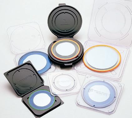
WEDGE & BALL BONDING WIRE Stocked in USA www.TanakaWire.com HIGH REL • DEFENSE • POWER GOLD 4N AND 2N www.masterbond.com +1.201.343.8983 ∙ main@masterbond.com SILVER CONDUCTIVE, LOW OUTGASSING SILICONE ADHESIVE SILVER CONDUCTIVE, LOW OUTGASSING SILICONE ADHESIVE Two Part, Addition Curing System MasterSil 151S NASA LOW OUTGASSING APPROVED Passes ASTM E595 tests ELECTRICALLY CONDUCTIVE Volume Resistivity 0.004 ohm-cm RESISTS AGGRESSIVE THERMAL CYCLES & SHOCKS
Assembly Solutions for Cost-Effective Heterogeneous Integration with Disparate Die Types
Glenn Farris Vice President of Strategic Marketing Universal Instruments

THE SEMICONDUCTOR INDUSTRY is driving to enable high volume integration of disparate die types via Heterogeneous Integration. These die can come from a range of wafer sizes fabricated in different technology nodes. This emerging package type creates new challenges regarding assembly efficiency and yield. Traditionally, flip-chip assembly process flows have utilized a single placement tool for the placement of the single die type onto the target substrate. For applications with multiple die types, a series of placement tools have been configured in a production line, with each tool dedicated to placing a specific die type. This paper explores the implications of this type of solution in the era of Heterogeneous Integration. Impacts on product yield, throughput, manufacturing efficiency, and overall assembly cost will be explored for a broad range of Heterogeneous Integration die configurations. A novel approach to optimizing overall assembly economics will be proposed based on sensitivity analysis for the range of die types expected in these applications. The appropriateness of this novel approach will be explored for a range of packaging solutions, including Flip-Chip, 2.5D, 3D, and Fan-Out.
Introduction
While transistor scaling continues, the economic improvements derived from this scaling, typically referred to as “Moore’s Law,” have been diminishing. For example, over the past decade, at nodes below 22 nm, the associated costs to design and introduce new products have increased by a factor of 7.75. (Figure 1,[1]).

The prevailing packaging solution to address this challenge is called Heterogeneous Integration (H.I.). Many studies have focused on areas such as chip to chip signaling, power distribution, materials,
thermals, bonding metallurgy, and design methodologies. Interface open standards such as UCI Express [2] attempt to establish a common specification for H.I. implementation.
However, the economic implications for various placement tool process flow have not been assessed. Placement tool costs can be subdivided into five major categories: yield, equipment depreciation, operators, floor space, and equipment utilization.
The “pick and place” assembly of multiple disparate die in a heterogeneous integration package traditionally uses multiple placement tools. Each unique

tool is dedicated to placing a specific die type and/or wafer type. A novel approach is to execute the complete placement of all die types for a given Heterogeneous Integrated package within a single tool. As such, a sensitivity analysis for a broad range of die configurations can be assessed by modeling the impact on the five major cost categories for multiple dedicated placement tools versus a single tool solution.
H.I. Circuit Characteristics
Device Types and Quantity per Substrate
The number of devices per H.I. circuit ranges from a minimum of two device types and may be as high as eight unique devices. These die typically range in size from 0.5 x 0.5 mm up to 20 x 20 mm. The quantity of each die per substrate can range from one to as many as eight.
Each die has a specific function, ranging from processor to memory, to sensing, to data transmission. A typical configuration with four die types and a maximum of eight die for one die type is shown in Figure 2.
Substrate Size and Quantity
Substrates upon which devices are
12 | MEPTEC REPORT SPRING 2023 meptec.org
ASSEMBLY
Figure 2. Typical HI device configuration.
Figure 1. Design cost by node.
mounted can range from traditional singulated high-density interconnect (HDI) organic to singulated silicon interposers to a substrate-less Wafer or Panel fan-out. In the case of singulated organic substrates, these are typically presented to the “pick and place” assembly tool via a JEDEC standard tray (or Gen2 JEDEC tray in the future). At substrate dimensions up to 31 x 44mm, up to 28 circuit substrates can be loaded in one JEDEC tray (Figure 3). Future Gen2 JEDEC trays can hold up to 56 of these sized circuit substrates.
A substrate-less Wafer level fanout carrier offers an assembly area for approximately 38 of this sized circuit. In contrast, a JEDEC standard panel fan-out carrier with a 600mm x 600mm assembly area supports up to 247 of this sized circuit.
The number of circuits per carrier significantly impacts the throughput of a single-cell placement solution, as wafer exchange time is amortized over a much larger number of placements for a specific die type. (Table 1)


Pick and Place Tool Characteristics
Traditional die pick & place line solutions have been optimized based on the premise that a single die will be placed on a single substrate. This is the typical flipchip application, which is the dominant “advanced packaging” application in the market today.
In the case of Heterogeneous Integrated devices, the solution has been to configure multiple systems in series with each other. Each system is tooled and dedicated to a specific wafer type and die type. There are several challenges with this approach.
The first challenge is that the line is unbalanced, as some systems may be placing eight or more devices, while some could be placing only one die (or even zero devices if there are more systems than die types to be placed). This results in an overall “effective throughput” per system that is as low as 13% of a single system solution. Constant re-arranging of the line would be required to optimize the assembly flow for different H.I. circuit configurations, which is impractical in a production environment. (Figure 4)
The second challenge is that the constant flattening and then flexing of the substrate can cause die float, as can movement out of and into multiple systems, impacting placement accuracy. Finally, moving substrates between eight dedicat-
ed systems in a line increases placement, fiducial find, and potentially temperature variability, further degrading placement accuracy. Based on typical system variability data, it is estimated that all these factors will increase the defective place-
ment parts per million (ppm) per device from a typical value of 100 ppm to 400 ppm for a 4-die H.I. device.
The third challenge is that increased operator attention will be required per line with up to eight machines in a line,
SPRING 2023 MEPTEC REPORT | 13 meptec.org
Figure 3. JEDEC Tray with 28 Substrates.
Table 1. 31mm x 44mm circuit capacity by carrier type.
Figure 4. Single System vs. Multiple Dedicated System Line.
as will increased floor space. This will increase the overall operational expense (OPEX) cost for the line proportional to the number of systems in the line.
The fourth challenge is utilization. Creating dedicated lines per circuit configuration versus a single cell that can handle any circuit will reduce typical utilization. In addition, material scheduling and downtime typically reduce a singlesystem solution to 85% utilization. With a 4-system solution, these “multi-system” factors are expected to reduce utilization further to, at best, 60%.
Throughput Sensitivity Analysis
To better understand the overall impact of these various parameters on Heterogeneous Integration assembly economics, a mathematical model was created to allow for a comprehensive sensitivity analysis.
As mentioned, the most critical factors are the time it takes to automatically change wafers and change associated end effector tooling to support a new die type, the number of circuits to be assembled per carrier, and the number of unique die types to be assembled per circuit.
Impact of Circuits per Carrier and Wafer & Tooling Change Time
Table 2 summarizes the relative throughput of assembled circuits for a Single System per Circuit solution vs. a Single Die per System solution. The comparison is made both for a Single System solution configured with a single wafer table as well as a Single System solution configured with dual wafer tables. The time to exchange unique wafers and end effector tooling (used for picking up the individual dies) for unique die types was varied from 15 seconds to 60 seconds. For this example, it was assumed the circuit had four unique die types, with quantity of die per die type of 8, 4, 2, or 1 respectively.

From Table 2, it can be seen that over the full range of scenarios for circuits per carrier and wafer + tooling exchange time, a Single System per Circuit solution delivers superior throughput. This advantage ranges from 12% in the corner case of only 4 circuits per carrier and 60-second wafer + tooling exchange time on a Single Wafer Table system up to
93% advantage when there are 1,024 circuits on a carrier and an exchange time of only 15 seconds.
Impact of Number of Die Types and Counts per Circuit
The impact of the number of unique die types per circuit and the quantity of each die type on the relative throughput of each solution type was also analyzed. This analysis was done for a fixed number of 28 circuits per carrier and a 30-second wafer + tooling exchange time.
As shown in Table 2, a Dual Table system, on average, doubles the relative throughput of a Single Cell per circuit solution. Generally, the placement speed
doubles and the time spent exchanging wafers + tooling is cut in half, resulting in this improvement. The Single and Dual Table Single System per Circuit solutions exhibits a 60% to 90% improvement in throughput in this example.
Secondly, the overall variation from 2 to 4 to 8 unique device types has much less impact than the number of circuits per carrier noted in Table 1.
Finally, the relative quantity of each unique die type has a more significant impact than the number of unique die types, mainly due to a greater impact on the total number of die on the circuit.
(Figure 5)

14 | MEPTEC REPORT SPRING 2023 meptec.org ASSEMBLY
Figure 5. Relative Throughput as a function of the Number of Unique Die types and Quantity per Die type.
Table 2. Relative throughput as a function of circuits per carrier and wafer exchange time.
Economic Model Summary
An economic model was created to assess the economic impacts of yield, depreciation per circuit, OPEX, and utilization. Pricing for a single wafer table Single System per Circuit solution was arbitrarily set to one million dollars. The price per machine for the single dedicated system per die type solution was set at $500 K.

A key observation from the economic model is that, while depreciation cost per assembled circuit is the typical factor used for solution comparison, the assembly yield has a much larger impact on the overall cost of manufacturing. (Table 3)
For the single bay Single System per Circuit solution, the depreciation cost is only 30.7% of the total assembly cost.
Two other factors heavily influence total assembly cost: total scrap per unit produced and operator cost. Operator cost is assumed to be directly proportional to the number of systems. Based on an estimated increase in defective placements from 100 ppm to 400 ppm for a four-die H.I. device, the increased scrap cost for the multi-system solution is more than the depreciation cost for the Single System per Circuit solution.
The economic model shows that even if the multi-system solution is free, the increased scrap, operator, and utilization costs result in the single-system solution delivering a 60% lower overall assembly cost.
Conclusion
In conclusion, with the advent of high-volume Heterogeneous Integration circuits, efficient advanced packaging assembly solutions are critical to optimizing the overall economics. A comparison of traditional assembly processes, which require a dedicated assembly system per die type, to a novel solution utilizing a single assembly system for all die, demonstrates a 60% cost of assembly advantage for the single-system solution. ◆
Author Biography
Glenn Farris joined Universal in 2013 as Vice President, Marketing and has been instrumental in leading the company to develop a strategic relationship with some of the world’s most prominent technology leaders. Glenn holds an MBA in Marketing and Finance from Santa Clara University, M.S. in Engineering
from Stanford University, and a B.S. in Engineering from Purdue University. Email: glenn.farris@uic.com
Acknowledgments
The author wishes to acknowledge this novel solution’s inventors and patent holders: Mike Yingling, Sean Adams, David Lyndaker & Scott Proctor – all employees of Universal Instruments.[3]
References
[1] IBS. As Chip Design Costs Skyrocket, 3 nm Process Node Is in Jeopardy. 2020. Available online: https://www.extremetech. com/computing/272096-3nm-process-node
[2] UCIe 1.0 Specification is an open industry standard developed to establish a ubiquitous interconnect at the package level. Available online: https://www.uciexpress.org/specification
[3] High-Speed Wafer Feeder Patent Number: 11164765 Issue date: 11/2/2021
Title: Modular Die Handling System
Inventors: Mike Yingling, Sean Adams, David Lyndaker, Scott Proctor
SPRING 2023 MEPTEC REPORT | 15 meptec.org
Table 3. Economic Model for H.I. Assembly.
Catching Up with Françoise
von Trapp
Editorial Director and Queen of 3DInCites.com
Owing to a very diverse and accomplished association of MEPTEC members, there are many informative, instructional, and entertaining stories to be told. “Catching Up With...” will feature stories from and about our members.
Françoise von Trapp (https://www. linkedin.com/in/fvontrapp/) is a well know industry contributor and has been involved with advanced packaging for almost twenty years. This interview was conducted via email and edited for clarity. Let’s start with what you are currently doing… You have been the Editorial Director and Queen of 3DinCites.com for over fourteen years now. First, would you tell us how you see 3DinCites as a community and what is different about it from other organizations in the world of advanced packaging?

What began in 2009 as a single blog focused on 3D integration technologies grew to an entire community focused on advancing heterogeneous integration and packaging, including 3D and chiplets. What sets us apart from other trade publications and industry organization is our focus not only on the technologies, but the people that make them happen. That’s one reason we’ve added initiatives in sustainability and Diversity, Equity and Inclusion (DEI). These are important topics to the future of our planet, and we want to make sure they are part of the semiconductor manufacturing conversation.
Our membership represents the entire supply chain, including some market research organizations, consultants, a public relations (PR) agency, and other industry organizations – both IMAPS and SEMI are community members. We offer a little bit of everything, from our own expert bloggers to member contributed
Launched in 2013, this photo was taken at the Awards Ceremony for the 2016 3D InCites Awards. In 2018, the awards ceremony moved from SEMICON West to IMAPS Device Packaging Conference.
https://www.3dincites.com/2016/07/and-thewinners-of-the-2016-3d-incites-awards-are/
articles, white papers, blog posts, and videos. The 3D InCites Awards are recognized as a prestigious industry award. Our latest addition is the 3D InCites podcast, now in its third season. Collectively, our 83 (and counting) episodes have been downloaded almost 10,000 times, and our listeners span the globe.
No one died (that we know of) that you succeeded to become Queen. Did you wake up one day and decide to be “Queen”? Or more importantly, how did you decide that you wanted to focus on 3D ICs? And how do you see that role differently than positions described by more traditional title?
Mike Plisinski, CEO of Onto Innovation sits down with Françoise at SEMICON West 2021, held in December of 2021 – as the event returned to a live event after COVID. 2023 will be the third SEMICON West that the 3D InCites Podcast is the Official Podcast of SEMICON West.


https://www.3dincites.com/2021/12/live-fromsemicon-west-hybrid-2021-its-the-3d-incitespodcast/
That’s a funny story. I would never be so arrogant as to crown myself queen. In 2007, 3D integration technologies were just emerging into the conference circuit. At the time, I was Managing Editor at Advanced Packaging Magazine. While attending SEMICON Europa, I was focusing my interviews on anything to do with 3D – through silicon vias (TSVs) were a hot topic. Lots of the tool vendors were showcasing their capabilities to support TSV processes. The EMC 3D Consortium was going full steam, and it provided a lot of information. As I walked into the SUSS MicroTec booth, Birgitta Wehrman, who lead their product marketing for lithography, announced: “Here comes the Queen of 3D!”. It had a nice ring to it –and it stuck. When the magazine folded and I lost my job, I decided to leverage that to build my personal brand.
When you were working on your Communication / Journalism degree from the University of New Hampshire did you know what industries you wanted to work in?
Initially, I wanted to get into mainstream journalism – feature writing or maybe trav-
16 | MEPTEC REPORT SPRING 2023 meptec.org
INTERVIEW
el. I was not serious about a career path. I wanted to live in Vermont and moved there and figured I’d find something there. I did a project for a gardening publication called Harrowsmith. Ultimately, I ended up working in food and beverage, in marketing at the Trapp Family Lodge, my family’s resort. I also spent some time running a bed and breakfast in southern Vermont.
Obviously, technology and “hanging out” with geeks & nerds is a far cry from your college internship at Teenage Magazine. Is there anything specific that you learned then that is relevant today or that you apply to your day-to-day work now?
I learned how a publication works. I learned about the process of putting a magazine together. I also learned how to write to a tone of voice. Ironically, it was that internship that landed me my Associate Editor job ad Advanced Packaging, more than 20 years later. Gail Flower, Advanced Packaging’s Editor and Chief, looked at my resume and commented that most of my experience was in marketing, and it would help if I had some editorial experience beyond the college newspaper. I suddenly remembered the internship and sent her some writing samples from there.
Many organizations across the microelectronics industry are focusing on DEI and sustainability because it’s become critical to environmental social governance (ESG). We’ve partnered with SEMI, IMAPS, and IEEE to help raise awareness about DEI at industry events. Society of Women Engineers is another notable
in advanced packaging, if you had a magic wand - or should I say full use of an imperial scepter – what should we change immediately to increase the number of women in the industry? And with this are there any small changes that each of us can do to improve the situation?
In 2022, 3D InCites held its first Hike for DEI, on the last day of IMAPS Device Packaging Conference. The event, sponsored by KLA, helped raise $25K for the DEI Fund, established to help start-ups owned by women or underrepresented minorities grow and thrive.

I wish all it took was the wave of an imperial scepter, but I don’t think there is an easy fix. And while I may be a visible woman in the industry – that’s mostly because of the way I approach life and people. I didn’t have any kind of agenda, and I am not an expert on the topic. I only know what I’ve experienced. When I started SemiSisters, it was just this organic thing. In the beginning, I found this industry intimidating and I felt like a poser – I didn’t know anything about technology, yet here I was, expected to write about it. At conference networking sessions, I’d gravitate to the few women who attended the conferences, hoping they wanted to talk about anything but technology. After a few years of seeing the same faces and becoming friends with them, I joked about how they were my SemiSisters. It was my business partner, Martijn Pierik, who suggested we brand that and create a LinkedIn group.
Was
there something specific that got you interested in technology?
Honestly, I had no interest in technology beyond using it. I’m not an engineer, and I avoided STEM classes like the plague. Except for my high school chemistry class, I really had no affinity for science. I’ve always been interested in people and what makes them tick.
3DinCites has expanded its mission to include promoting and supporting diversity, equity, and inclusion (DEI) and environmental sustainability. Both are not only morally important but essential to the ongoing success of the semiconductor industry by enabling growth. With DEI one of the top challenges is getting women and other underrepresented groups into the industry at all levels. Are there any notable programs that increase women and minorities in science, technology, engineering, and math (STEM) that we should all be supporting?
https://www.3dincites.com/2022/03/takingstrides-for-dei-fund-raising-efforts-bring-in-25k/
organization promoting STEM education around the world. At 3D InCites, we’ve always donated a portion of our proceeds to STEM education, from the IEEE Frances B. Hugle Women in Engineering Scholarship, to the SEMI Foundation for SEMI High Tech U, as well as the IMAPS Foundation. In 2020, we decided to launch our own fund, the DEI Fund, to support tech start-ups owned by women and under-represented minorities, to help them grow and thrive. Unfortunately, over three years, we’ve only raised $63K. But we’ve got some ideas brewing on how to best leverage that. That’s a program we’d love support for. [Editor’s note: please contact Martijn Pierik at Martijn@3DInCites.com to support this great program.]
And as a long time “trailblazer” as one of very small number of visible women
But that’s not answering your question: what I’ve learned from the real experts in DEI is that there are so many different areas that need to be addressed. We need to inspire the next generation of workforce beginning in kindergarten, about how cool our industry is. We need parents to encourage their daughters not only to pursue careers in STEM, but engineering. We need college programs focused on semiconductors and microelectronics, not just engineering so that students understand what career paths are open to them with an engineering degree. In the workplace, we need to go beyond mandatory DEI training to implementing those learnings into our work cultures. We need flexible work schedules that accommodate working parents – both moms and dads. We need to focus on equity – not equality. Equality means giving everyone a bicycle. Equity is giving everyone the type of bicycle that they can ride.
SPRING 2023 MEPTEC REPORT | 17 meptec.org
Similarly on environmental sustainability, beyond adding it into our product definition and our corporate operations, are there programs and/ or personal small changes that you advocate for?
Again, I’m not an expert in these areas. In fact, we’ve brought in Julia Goldstein and Dean Freeman to blog about sustainability. However, I do know that we can’t do enough in our industry to help reverse climate change. Luckily, organizations like SEMI and imec have initiated sustainability programs. Most notably, SEMI’s Semiconductor Climate Consortia and its Semiconductor Startups for Sustainability initiative. Imec’s Sustainable Semiconductor Technologies & Systems (SSTS) research program. Personal small changes? Take shorter showers. Use less plastic. Take public transportation. Stop watering the lawn. Reduce, Reuse, Recycle. Read Julia Goldstein’s book, Rethink the Bins.
You’ve worked with a wide range of clients at Impress Labs that merged with Duo PR to become Kiterocket, marketing / public relations agencies, generating content and informing the industry and the public about their client’s products and technology. Any tricks or special approaches on how to translate their internal “techno babble” to content that can be understood by a wider audience?
I started as subject matter expert for the semiconductor clients, and when I left, I was Content and Creative Director.
The most important thing a company can do to be understood by a wider audience is avoid using technical and industry jargon and make your content relatable. Explain how it’s used in real-world applications. Speak in the first person and focus less on what you do and more on what it does for your customer.
Was your first introduction to semiconductor packaging when you were the Managing Editor of Advanced Packaging Magazine / Solid State Technology for PennWell? Semiconductor Packaging is a rather “niche” industry, was there something that drew you to it?
To be honest, I had no idea what a semi-
conductor or advanced packaging was when I was hired at Advanced Packaging. I needed a job. I was recently divorced and had 10-year-old twin daughters to raise. I was just getting back into the workforce full time. I had been freelancing for the past 10 years and had experience writing website content for all sorts of businesses. It was the only interview I
grandmother, as she was my father’s stepmother. During my lifetime, my father was a family physician, and he didn’t talk much about his days singing with the family during the war. But I can refer you to vontrapp.org where you can find lots of historical information.
Arizona is far away and a different place from New England where you grew up. What brought you to Arizona, what do you miss from New England?
It’s a Billy Joel Song – lost my job, sold my house, bought a ticket to the West Coast… well almost. I lost my job at Advanced Packaging and sold my house in Massachusetts. We needed to move somewhere, and Arizona was more affordable than the Bay Area, yet close enough to participate in the semiconductor industry. Seemed like a good place to start 3D InCites. What I miss most? My daughter Jessie, who moved back to Boston after college and is now married. I don’t miss the weather.
https://www.3dincites.com/2017/02/highlights2017-european-3d-summit/

got and so I took the job – planning to build my resume. I figured I could do anything for a year! That was 2005.
The more I learned about the industry and the technology, the more interesting it became. What I liked about Advanced Packaging was that its tangible. I could understand it. Design and test are beyond me though – they are too esoteric. The reason I decided to focus on 3D technologies initially is that it was new to everyone – I figured it was easier to become an expert in something that nobody knew anything about than to get up to speed on legacy packaging technologies.
For those who haven’t already asked you, what would you like to share about your grandmother Maria von Trapp and your extended family history as reality is often distorted by Hollywood and Broadway?
My connection to the von Trapp family that was portrayed in the Sound of Music is that my father was the oldest of the original seven children. The musical and the movie were based on the book, the Story of the Trapp Family Singers, written by Maria von Trapp, who was my grandmother – or really my step-
Are you excited up all the upcoming semiconductor related investment in Arizona?
To be honest, I have mixed feelings about it. As excited as I am about the possibilities for our industry and the growth of 3D InCites, I’m concerned about the water supply in Arizona. I’m not sure it’s the best place for fab expansion. Just because we have the water rights to the Colorado River, doesn’t mean we have the WATER. You’ve done a fair bit of travel to different clients and conferences around the globe. What is your favorite place to visit for work? And any favorite places to travel to for fun?
I love Munich. I look forward to SEMICON Europa there every year. My favorite place to travel for fun is Costa Rica. My husband and I eloped there in January. It was our second trip. I think it’s going to become an annual event.
Are there any particular hobbies or leisure activities that you enjoy?
I love to cook and entertain. I love being outdoors and spend as much of the year outside as I can, hiking, cycling, walking, swimming…and I recently took up golf ◆
18 | MEPTEC REPORT SPRING 2023 meptec.org INTERVIEW
The lighter side of the industry – one of our first SemiSister group photos taken at the 3D Summit Gala Dinner in Grenoble, France in 2017.


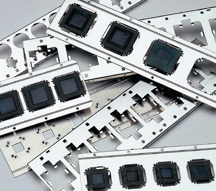
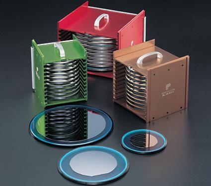
MONSTERPAC® 80 170℃ Flip Chip Bonding URL: http://www.ConnecTec Japan.com E mail: sales@ConnecTec Japan.com Seoul / Sales Office #16229, 1109Room, Ace Gwangyo Tower2, 1286-1, Iui-Dong, Yeongtong-Gu, Suwon-Si, Gyeonggi-Do, KOREA San Jose / Sales Office 2033 Gateway Place,5th Floor, San Jose, CA 95110, USA OSRDA : Out Sourced R&D and Assembly Niigata / Head Office, R&D and Factory 3-1 Koudan-cho, Myoukou City, Niigata, JAPAN 944-0020 Phone: +81-255-72-7020 Tsukuba / R&D Laboratory By connecting various technologies, we provide comprehensive support and services for customer needs through cooperation with our affiliates & partners. MEMS/Bio/Photonics Flexible PET/PEN/PU Fine Traces/Bumps Large Die


Perfection Products Inc. 1320 S. Indianapolis Ave. • Lebanon, IN 46052 Phone: (765) 482-7786 • Fax: (765) 482-7792 Check out our Website: www.perfection-products.com Email: sales@perfection-products.com Grip Ring Shippers I. C. TraysMulti-Channel Lead Frame Magazines - F.O.L./E.O.L. Film Frame Magazines Film Frames Film Frame Shippers TO Tapes & Magazines Magazines and Carriers for Process Handling Solutions Accept Nothing Less. Substrate Carrier Magazines Stack MagazinesE.O.L. Wafer Carriers Process Carriers (Boats) Boat Magazines Grip Rings Miscellaneous Magazines I. C. Tubes and Rails Grip Ring Magazines

