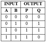
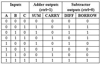
Table-1:TruthTableof
Fig 2
2.1
© 2022, IRJET | Impact Factor value: 7.529 | ISO 9001:2008 Certified Journal | Page51
Reversiblelogicisoneofthepractical programforpower efficient. As per R. Landauer when one bit of information losses, KTln2 joules of energy dissipate where, K is the Boltzmann’sconstantandTistheoperationaltemperature. Afterthis,Bennetthadprovedthatthisenergycanbesaved by using reversible logic. In point of fact, when the inputs cannot be recovered from circuit’s outputs, loss of informationwillbeappeared.Whereas,Reversiblelogicwill handlethisproblem.Thislogic,onetoonemappingbetween theinputsandoutputs.
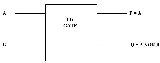
Inthisproposedwork,wehavedesignedhybridfulladder and full subtractor using Feynman gate and TR gate. FeynmangateandTRgateisdesignedusingpastransistor logic. Feynman Gate :BlockDiagramofFeynman(FG)gate. FeynmanGate.
International Research Journal of Engineering and Technology (IRJET) e ISSN: 2395 0056 Volume: 09 Issue: 01 | Jan 2022 www.irjet.net p ISSN: 2395 0072 HAS: HIGH SPEED & POWER EFFICIENT HYBRID ADDER/SUBTRACTOR DESIGN USING REVERSIBLE LOGIC Rushitha. K1, K. Vandana2, K. Mallika3, M. Jagath Chandra4, Somashekhar Malipatil5 1 4B.Tech Scholar, Department of ECE, Malla Reddy Engineering College and Management Sciences, Medchal, Hyderabad 5Associate Professor, Department of ECE, Malla Reddy Engineering College and Management Sciences, Medchal, Hyderabad *** Abstract Reversiblelogicisextensivelycontemplatingasthe potential logic design style for execution in modern technologies. Such as, nanotechnology and QC. In this paper, we have designed hybrid full adder and full subtractor using Feynman gate and TR gate. Feynman gate and TR gate is designed using pas transistor logic. The simulation results show the high speed, decrease in size and lower power dissipation can be realized with the HAS: Hybrid Adder/Subtractor design using reversible logic. The schematicsare analyzedinDSCH2andLayoutsaredesigned andinMICROWIND2.weimprovedthespeed1ps,power6.23mW,area74.504mm2. Key Words: Reversiblelogic,Feynmangate,TRgate,Power dissipation,FullAdder,FullSubtractor. 1.INTRODUCTION
2. PROPOSED
Fig 1:n*nReversibleLogic. WORK

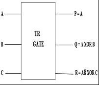
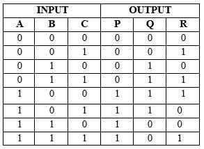
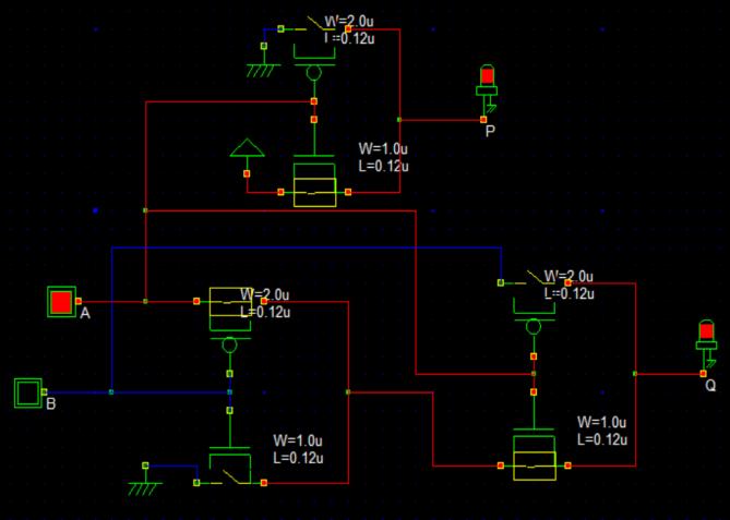
TheaboveFigurerepresentstheschematicofhybridTRgate with A, B, C as inputs and P, Q, R as outputs, where P=A, Q=A⊕BandR=AB’⊕C.ThisgateisproposedbyToffoliand Ranganathan.Thefigure12showstheCMOSrealizationof TRgate.ThepasstransistorrealizationofTRgateisshown in above figure Consider the inputs are a=‘1’, b=‘1’, c=‘0’. Since a=‘1’ the transistor Q1 is OFF and Q2 is ON. So the outputp=‘1’.Sincea=‘1’andb=‘1’,Q4,Q8areONandQ3,Q7 are OFF. So the ground value ‘0’ is passed through Q4, Q8 thentheoutputq=‘0’.Sincea=‘1’,b=‘1’andc=‘0’,thenQ6,Q9, Q12areONandQ5,Q10,Q11areOFF.Sothegroundvalue ‘0’ispassedthroughQ10,Q12thentheoutputr=‘0’.
2.2 TR Gate
Fig 4:BlockDiagramofTRgate.
Table TruthTableofTRGate
2:
Fig-3:SchematicofFGGate
TheabovefigureshowsschematicoftheFeynman(FG)gate. The Feynman gate is also known as controlled not gate (CNOT). Ithastwoinputsi.e.,AandBandtwooutputsi.e.,P andQ.TheoutputsaregivenasP=A,andQ=AXORB.which realizes XOR gate with a garbage output ‘A’. If B=‘0’ it replicates the input ‘A’ and if B=‘1’, then it transpose the input‘A’totheoutputQ.Thepasstransistorrealizationof Feynmangateisshowninfigure2.Considerinputsasa=‘1’ andb=‘1’,thenthetransistorsQ2,Q4andQ6areONandthe remainingtransistorsareOFF.SotheVddvalue‘1’isdirectly passedtotheoutput‘p’andthegroundvalue‘0’ispassedto theoutputq.So,p=‘1’andq=‘0’
International Research Journal of Engineering and Technology (IRJET) e ISSN: 2395 0056 Volume: 09 Issue: 01 | Jan 2022 www.irjet.net p ISSN: 2395 0072
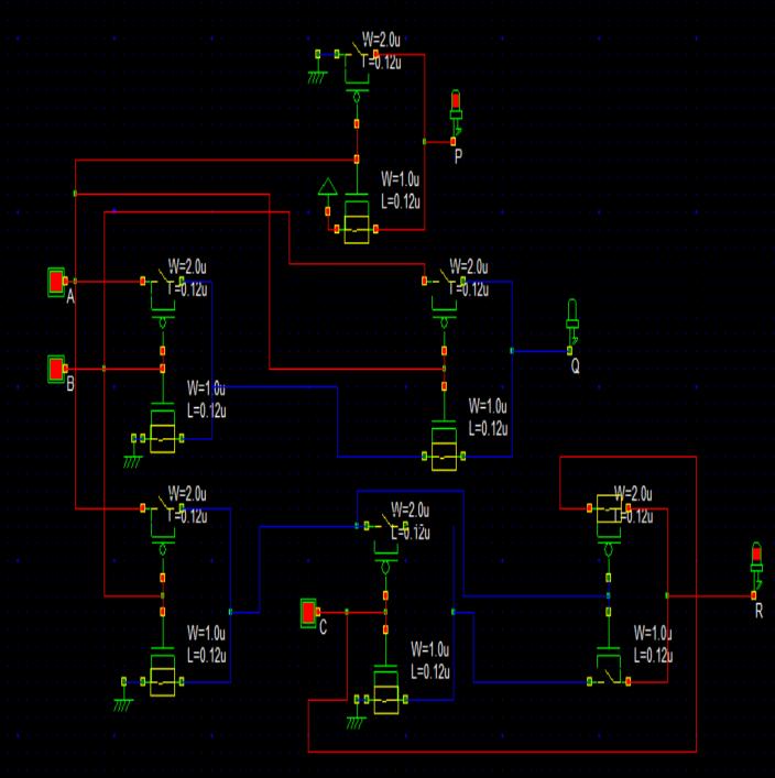
Fig 5: SchematicofTRGate
© 2022, IRJET | Impact Factor value: 7.529 | ISO 9001:2008 Certified Journal | Page52
3
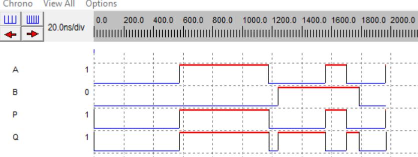
Whenthecontrol(CTRL)isinONconditionitactsasa halfadderi.e.,CTRL=1.Whenwegiveinputas‘0’totheboth inputsAandBweget‘0’asaoutputinbothsumandcarry i.e.,bothLEDswill beinoff condition.Similarly,Whenwe giveinputs‘0’and‘1’totheAandBthereforetheoutputs willbe‘1’insumand‘0’incarryi.e.,sumLEDwillbeONand carryLEDwillbeOFF.When1and0inputsaregiventoA& BthesumLEDswillbeONandcarrywillbeOFF.Giving1to AandBinputssumLEDwillbeOFFandcarryLEDwillbe ON. Whenthecontrol (CTRL)isinOFF conditionitacts halfsubtractori.e.,CTRL=0.InthiswhenA&B takenas‘0’ thedifference/BorrowwillnotbeinONstatei.e,LEDisin OFF.WhenAistakenas‘1’andBistakenas‘0’hence, it's difference LED will be ON and borrow LED will be OFF. WhenAistakenas‘0’andBistakenas‘1’thedifferences LEDwillbeONandborrowLEDwillbeOFF.WhenAandBis takenas‘1’thedifferenceandborrowLEDswillbeOFF.
Table :TruthTableofHybridHalfAdder/Subtractor
Fig-7: SchematicofHybridHalfSubtractor
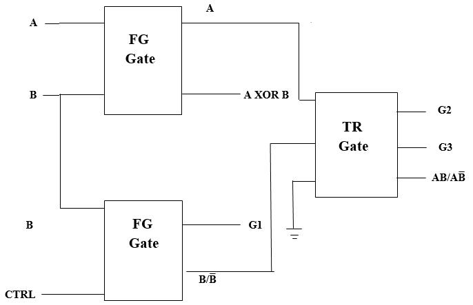
Fig-6: BlockDiagramofHybridHalfAdder/Subtractor
Fig 8: SchematicofHybridHalfAdder.
In the hybrid half Adder/Subtractar we use two differenttypesofGates:whicharenamelyFEYNMANGate andTRGate.Theaboveschematicshowsthecombinations oftwoFGgate’sandwithoneTRgate.WhereoneFGgate hastwoinputsandtwooutputs,inthisFG1gateofBinputis connectedtoFG2gateof1st inputasshowninaboveFigure and2ndinputistakenascontrolgate.Thiscontrolgateis switchestooneandzero basedonitsinput,itactsashalf adder/subtractar. The FG 1 gate of Q output is connected withaLEDthatshowstheSum/DifferenceandFG1gateofP output is connected to the input of TR gate as shown in above figure. Although, the FG 2 gate of Q output is connected to B input of TR gate and TR gate C input is connectedtoground,sinceoutputistakenoutfromRwith LEDwhichisCarry/Borrow.
Inputs Adder (Ctrl=1)Outputs OutputsSubtractor(Ctrl=0) A B Sum Carr Y Diff Borrow 0 0 0 0 0 0 0 1 1 0 1 1 1 0 1 0 1 0 1 1 0 1 0 0 © 2022, IRJET | Impact Factor value: 7.529 | ISO 9001:2008 Certified Journal | Page53
International Research Journal of Engineering and Technology (IRJET) e ISSN: 2395 0056 Volume: 09 Issue: 01 | Jan 2022 www.irjet.net p ISSN: 2395 0072 2.3 Hybrid Half Adder/Subtractor
Adder
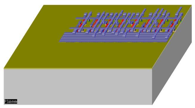
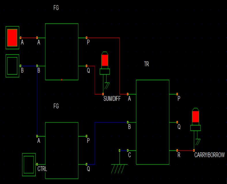
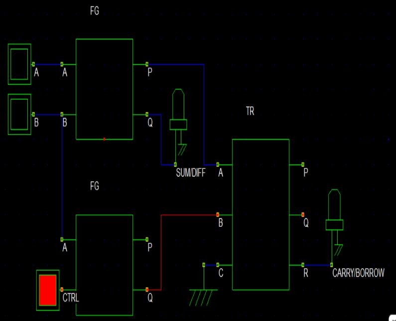
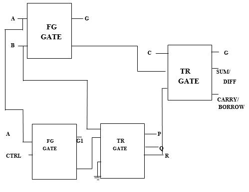
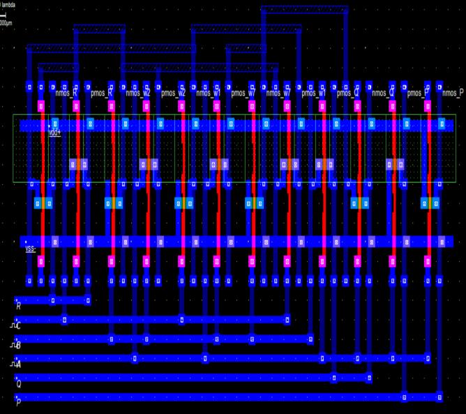
International Research Journal of Engineering and Technology (IRJET) e ISSN: 2395 0056 Volume: 09 Issue: 01 | Jan 2022 www.irjet.net p ISSN: 2395 0072 2.4 Hybrid Full Adder/Subtractor Fig 9: BlockDiagramofHybridFullAdder/Subtractor
Sum/DifferenceistakenoutfromthesecondTRgatewhere isLEDisconnectedandCarry/Borrowistakenoutfromthe secondTRgatewhereanotherLEDisusedheretoindicate the operations of full adder and full subtractor. When the inputsaregiven000asinputtheoutputwillbe00insum andcarry&viceversa.Whentheinputsaretakenas001,010 and 100 the sum will be in ON so that LED will turn ON. Whentheinputsaretakenas011,101,110thecarrywillbe in ON. Coming to Full subtractor it is also provide same outputif the3inputsaresame,thentheoutputwillbethe input as same the inputs. When the inputs are taken as 001,010theoutputwillbeturnedonsotheLEDwillbeONIf theinputis011thenonlyborrowoutputwillbeturnedon andwhentheinputis100thendifferenceoutputwillbeON.
4:
Fig-10: SchematicofHybridFull
3. 3.1RESULTSSimulationsFig 12: SimulationofFGGate © 2022, IRJET | Impact Factor value: 7.529 | ISO 9001:2008 Certified Journal | Page54
WhentheControlisinONstateitactsasFulladder,Ainput inFGgateisconnectedtofirstinputofsecondFGgateandB inputinFGgateisconnectedtoTRfirstinput.Cistakenas thirdinputfromsecondTRgate.TheoutputsofFGgateand TRgateisconnectedtosecondTRgateasshowninfigure.
Fig 11: SchematicofHybridFullSubtractor.
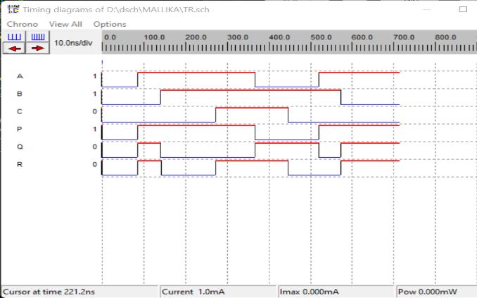
The above figure shows the schematic of the Full Adder/Subtractor.InthisoperationweusetwoFGgatesand two TR gates with Three inputs that are A,B and Control.
Table TruthTableofHybridFullAdder/Subtarctor
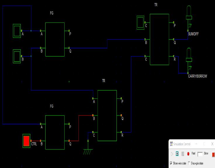
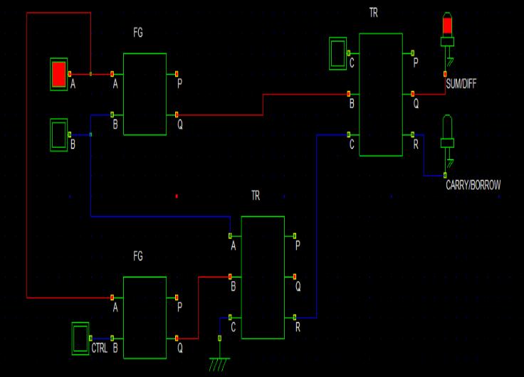
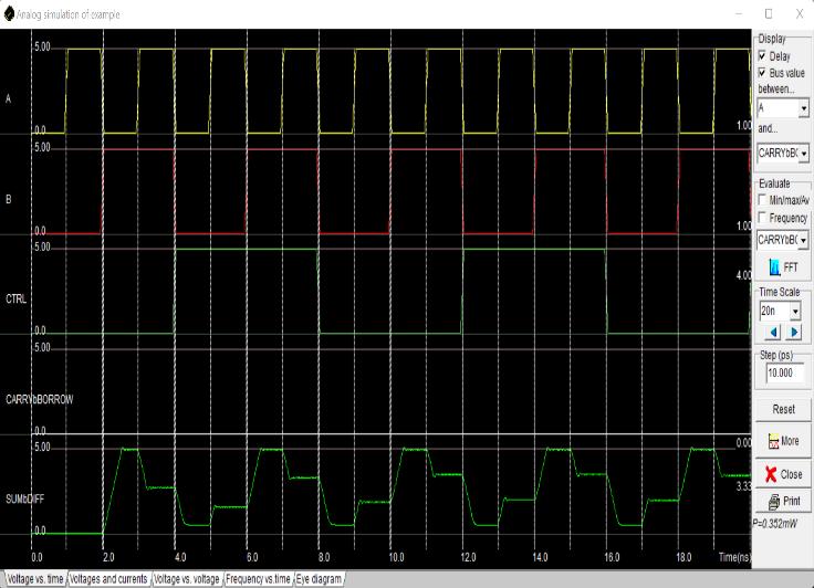
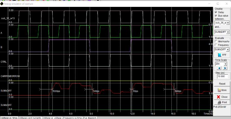
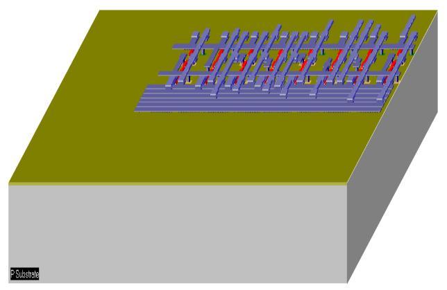
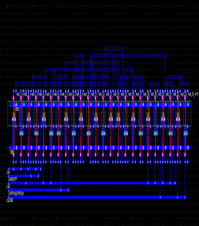
International Research Journal of Engineering and Technology (IRJET) e ISSN: 2395 0056 Volume: 09 Issue: 01 | Jan 2022 www.irjet.net p ISSN: 2395 0072 Fig-13:SimulationofTRGate Fig-14: AnalogSimulationofhalfAdder/Subtractor Fig 15: AnalogSimulationofHybridfullAdder/Subtractor 3.2 Layouts and 3D views Fig 16: LayoutofHybridHalfAdder/Subtractor Fig 17: 3DviewofHybridFullAdder/Subtractor Fig 18: LayoutofHybridFullAdder/Subtractor © 2022, IRJET | Impact Factor value: 7.529 | ISO 9001:2008 Certified Journal | Page55
© 2022, IRJET | Impact Factor value:
Certified Journal | Page56
[5] SomashekharMalipatil,R.BasavarajuandPraveen Kumar Nartam. "Low Power & High Speed Carry SelectAdderDesignUsingVerilog"IOSRJournalof VLSIandSignalProcessingVol.6Iss.6(2016)p.77 81ISSN:2319 4197.
[7] Somashekhar Malipatil, Avinash Gour and Vikas Maheshwari, Design & Implementation of ReconfigurableAdaptiveFaultTolerantSystemFor ALU,InternationalJournalofElectricalEngineering andTechnology,11(9),2020,pp.01 07.
| ISO
[9] P.KaurandB.Dhaliwal,Designoffaulttolerantfull adder/subtractor using reversible gates, in ComputerCommunicationandInformatics(ICCCI), 2012.
[4] J.Bruce,M.Thornton,L.Shivakumaraiah,P.Kokate, and X. Li, Efficient adder circuits based on a conservative reversible logic gate, in VLSI, 2002. Proceedings. IEEE Computer Society Annual Symposiumon,2002,pp.7479.
[6] Somashekhar Malipatil, Avinash Gour, Vikas Maheshwari, FPGA Implementation of Fault Tolerant & High Speed Reversible Systolic Multiplier Volume 09, Issue 12, Pages: 537 542. DOI:10.48047/IJIEMR/V09/I12/95.
International Research Journal of Engineering and Technology (IRJET) e ISSN: 2395 0056 Volume: 09 Issue: 01 | Jan 2022 www.irjet.net p ISSN: 2395 0072 Fig 19: 3DViewofHybridFullAdder/Subtractor 3.3 Power Analysis HybridHalf 0.352mwatts.Adder/Subtractor HybridFull 6.253mwattsAdder/Subtractor 3.4 AreaHybridAnalysisHalf Adder/Subtractor Area=376um*129um=48.504mm 2 Hybrid Full Adder/Subtractor Area=556um*134um=74.504mm 2 3.5 Delay Analysis 1pz 4. CONCLUSION In this paper, we have designed hybrid adder/subtractor usingreversiblelogic.wehaveenhancedthespeed1psand optimized the power 6.23mW and area 74.504mm2 . The totallayoutisreducedbyusinglessnumberoftransistors andsimulatedinMicrowind2. REFERENCES [1] R.Landauer.,Irreversibilityandheatgenerationin thecomputingprocess,IBMJournalofResearchand Development,vol.5,no.3,pp.183191,July1961. [2] C.Bennett,Logicalreversibilityofcomputation,IBM JournalofResearchandDevelopment,vol.17,no.6, pp.525532,Nov1973. [3] S. K. S. Hari, S. Shroff, S. Mahammad, and V. Kamakoti, Efficient building blocks for reversible sequential circuit design, in Circuits and Systems, 2006. MWSCAS 06. 49th IEEE International Midwest Symposium on, vol. 1, Aug 2006, pp. 437441.
[8] D. Maslov, G. Dueck, and D. Miller, Synthesis of fredkin toffoli reversible networks, Very Large ScaleIntegration(VLSI)Systems,IEEETransactions on,vol.13,no.6,pp.765769,June2005.
[10]S. Malipatil, A. Gour and V. Maheshwari, "Fault Tolerant Reversible Full Adder Design Using Gate DiffusionInput,"2020InternationalConferenceon Smart Technologies in Computing, Electrical and Electronics (ICSTCEE), 2020, pp. 120 123, doi: 10.1109/ICSTCEE49637.2020.9276774.
[12]SomashekharMalipatil,VikasMaheshwariandR.P. Singh, "FPGA Implementation of Fault Tolerant Adder using Verilog for High Speed VLSI Architectures",InternationalJournalofEngineering and Advanced Technology (IJEAT), vol. 9, no. 4, April2020,ISSN2249 8958. 7.529 9001:2008
[11]S.Malipatil,V.MaheshwariandM.B.Chandra,"Area OptimizationOfCMOSFullAdderDesignUsing3t Xor," 2020 International Conference On Wireless CommunicationsSignalProcessingAndNetworking (Wispnet), 2020, Pp. 192 194, Doi: 10.1109/Wispnet48689.2020.9198627.