International Research Journal of Engineering and Technology (IRJET)
e-ISSN: 2395-0056
Volume: 08 Issue: 09 | Sep 2021
p-ISSN: 2395-0072
www.irjet.net
Low Power SR-Latch Based Flip-Flop Design Using 21 Transistors Kinga Lhaden Dakpa1, Thubten Jamtsho2, Kamal Kumar Chapagai3 1,2,3Dept.
of Electronics and Communication Engineering, College of Science and Technology, Bhutan ---------------------------------------------------------------------***---------------------------------------------------------------------
Abstract - This paper proposes a design for an edge
could be simplified by using a newer logic which is described in this paper.
triggered flip-flop. The design is based on an SR latch and can be used in low voltage and low power applications. It uses a conventional NAND gate flip-flop design whose design flaw is eliminated by removing the redundant logic present in the design. The proposed circuit is designed and simulated using OrCAD PSPICE. The redundant logic was successfully removed with the circuit functioning as per its truth table. The newly designed flip-flop consumes a power of 83.47µW which implies a low power consumption. The proposed circuit can be expected to have a higher speed compared to the conventional design due to the reduction in the number of transistors.
In this paper, a newly presented design of an edge triggered flip-flop which is designed based on a SR Latch is verified. The design consists of six two-input NAND gates and a single-phase clock loading which generally starts increasing the clock signal loading. Due to the lower transistor count and a short circuital path in this design, a smaller layout area is obtained.
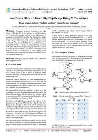
2. CONVENTIONAL DESIGN The conventional flip-flop consists of NAND gate-based SR latch flip-flop consisting of 5 two-input NAND gates and a three-input NAND gate as shown in the Fig. 1.
Key Words: NAND gate, flip-flop, ORCAD, PSPICE, SR latch, edge triggered device
1. INTRODUCTION Electronics use flip-flops (FF) to store data. Flip-flops or latches are circuits that can remember the information of a state, which allows it to be used as memory. Their efficiency depends on the power consumption and the overall chip area. Therefore several methods has been implemented to achieve low power consumption such as reducing the supply voltage. For flip-flops, at low supply voltages their performance degrades, therefore supplying a low voltage is not viable for flip-flops design [1]. The design of flip-flops has constantly evolved over the years, based on their target applications. In this paper, the flaws of some classic flip-flop design are studied and a newly proposed efficient design that can be applied in low power applications has been verified.
Fig -1: Conventional edge triggered flip-flop [5] Table -1: Truth table of Conventional Edge Triggered Flip-Flop
One of the leading flip-flop designs in the industry is the Transmission gate-based Master Slave flip-flop [2]. This design relies heavily on the clock which increases its workload along with the requirement of inverters to invert clock signals, which leads to more power consumption [3]. A NOR type SR latch-based flip-flop has been proposed recently [1]. However, the requirement of inverted clock signals and the stacked PMOS structure increased its power consumption [4]. The traditional design uses three-input NAND gates which increase the number of transistors and has a redundant logic in the circuit [5]. The redundant logic in the circuit
© 2021, IRJET
|
Impact Factor value: 7.529
D
CLK
X2
X3
Q
0
0
1
1
P
P’
1
0
1
1
P
P’
0
1
0
1
0
1
1
1
1
0
1
0
In Table 1, P refers to Previous State and P’ refers to the Opposite of Previous State.
|
ISO 9001:2008 Certified Journal
|
Page 1699