International Research Journal of Engineering and Technology (IRJET)
e-ISSN: 2395-0056
Volume: 08 Issue: 08 | Aug 2021
p-ISSN: 2395-0072
www.irjet.net
Comparison of various Techniques of 1-bit Full Adder in Cadence 90nm Technology Rahael More1, Meghana Khare2 1Mtech,
Department of Electronics, Walchand College of Engineering, Sangli Meghana Khare, Department of Electronics, Walchand College of Engineering, Sangli ---------------------------------------------------------------------***---------------------------------------------------------------------along with power there is a need to reduce delay as Abstract - Digital circuits have a most common component well. called as full adder which performs operations of arithmetic 2Mrs.
such as summation and subtraction. This paper compares as well as analyzes and calculates evolution of different full adders which are constructed using various logic styles. These full adders are analyzed based on power consumption and delay. Here CMOS, Hybrid CMOS, PTL, 10 SERF and 10T GDI are presented. The width of NMOS is 120nm and that of PMOS is 240nm respectively in cadence 90nm technology. 10T SERF and 10T GDI which are included here are the two full adders which are most popular design of full adder. It consists of minimum transistor count as well as less delay and low power when compared with previously constructed full adder designs. The implementation is done in cadence virtuoso. Comparison of these full adders based on power and delay is the major objective. The results and experimental values of power, delay, propagation delay and capacitance are shown in tabular form at the last part. The final full adder which results in less power and delay is further extended to Arithmetic Logic Unit as one of its application.
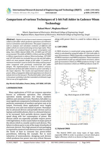
1.1 28T CMOS A CMOS structure is constructed using equation of adder which is calculated by using full adder of 1-bit truth table. It uses 28 transistors. CMOS is basically a combinational circuit of PMOS transistors and NMOS transistors. These transistors are represented as pull-up and pull-down structure, where pull-up transistors which are PMOS produces strong ‘1’ and pull=down transistors which are NMOS produces weak ‘0’.
Key Words: Full adder, Power, Delay, 10T SERF, 10T GDI.
1.INTRODUCTION Many applications of VLSI use common operation known as arithmetic operation. This arithmetic operation mainly operates two binary numbers addition and calculates it sum. Therefore, full adder is a most significant component of arithmetic circuits which performs summation of numbers and gives sum at its output. Previously these applications were largely focused on area and cost instead of power. Nowadays due to advanced devices and portable devices such as laptops and mobile phones, there is a demand of power to be increased. Such portable devices require high speed along with low consumption of power. But devices which are especially portable require power with high battery. It also causes failure in major parts of the silicon which is a mostly used in such devices. This failure in silicon parts is one of the major drawbacks of electronic devices. Very high amount of cost packaging is required to construct such devices in order to control the levels of heat to consume less power.within parentheses, following the example. But in most industries of semiconductor, designing such devices which produces low power was very critical. Because © 2021, IRJET
|
Impact Factor value: 7.529
|
Fig : Block diagram of 28T CMOS
Fig : Schematic of 28T CMOS
1.2 Hybrid CMOS The Hybrid CMOS uses many types of logic styles, especially CMOS in order to produce a circuit which gives higher efficiency which is as shown in Figure below. ISO 9001:2008 Certified Journal
|
Page 3493