International Research Journal of Engineering and Technology (IRJET)
e-ISSN: 2395-0056
Volume: 08 Issue: 06 | June 2021
p-ISSN: 2395-0072
www.irjet.net
Low Power Carry Skip Adder Design using Full Swing GDI Technique Akshatha K.S.1, Dr.H.V. Manjunath2 1PG
Student (M. Tech, VLSI Design and Embedded Systems), Dept of ECE, DSCE Bangalore, Karnataka 2Professor, Dept of ECE, DSCE, Bangalore, Karnataka ---------------------------------------------------------------------***---------------------------------------------------------------------
Abstract – The main parameters in any logic circuit designs
direct path static power dissipation. For this reason, FS-GDI technique came into existence.
are Power consumption and chip area. The full swing gate diffusion input (FS-GDI) technique is considered to be more effective for low power digital design supporting smaller area consumption and reduced power intake in contrast to CMOS technique. It also maintains a less complex logic design and with minimum transistors many logic gates can be designed. In this project comparison is done between conventional carry skip adder and proposed full-swing gate diffusion input (FSGDI) carry skip adder in terms of transistors count and power consumption. Schematic and implementation of project is done in cadence virtuoso at 45nm technology.
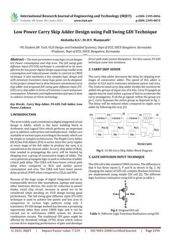
2. CARRY SKIP ADDER The carry-skip adder decreases the delay by skipping over stages of consecutive adder. The speed of this adder is similar to CLA and it consumes minimum power and area. The Uniform sized carry skip adder divides the words to be added into groups of equal size of k-bits. Carry Propagate pi signals may be used within a group of bits to accelerate the carry propagation. If all the pi signals within the group are pi=1, carry bypasses the entire group as depicted in fig. 1. The delay will be reduced when compared to ripple carry adder by following this way [1].
Key Words: Carry Skip Adder, FS-GDI, Full Adder, Low Power, Cadence
1.INTRODUCTION The most widely used constituent in digital integrated circuit design is Adder, which is the basic building block in Arithmetic and Logical Unit which performs an important part in addition, subtraction and multiplication. Adders are available in various types according to the needs; which can be simple or complex architectures. The Ripple Carry Adder (RCA) has Full Adders (FA) in series. Since the carry ripples in every stage of the full adder to produce the sum, it is considered as the slowest adder. In carry skip adder (CSKA), time needed in propagating the carry will be limited by skipping over a group of consecutive stages of adder. The carry generate propagate logic is used in reduction of adder critical path delay. The CSKA will have lesser critical path delay when compared to RCA and similar power consumption and area. The CSKA will have lesser power delay product (PDP) when compared to CSLA and PPA.
Fig-1: 16-Bit Carry Skip Adder Block Diagram
3. GATE DIFFUSION INPUT TECHNIQUE The GDI cell is like standard CMOS inverter. The difference is that it has three inputs G, P and N as shown in fig. 2. By changing the inputs of GDI cell, complex Boolean functions are implemented using simple GDI cell [2]. The different logic functions realization using GDI is given in table 1.
Because of the huge usage of digital integrated circuit in transportable devices like smartphone, laptops and many other electronic devices, the want for reduction in power intake, small chip circuit, increase in speed are to be considered while deciding on VLSI design having good performance. The full swing gate diffusion input (FS-GDI) technique is used to achieve low power and less area in comparison to various logic patterns using only 2 transistors. FS-GDI design method has become a promising opportunity other than static CMOS logic and it can be carried out in well-known CMOS system for diverse combination circuits. The traditional GDI gates might be afflicted by threshold voltage (VTH) drops which reduce current drive impacting performance of gate and develops
© 2021, IRJET
|
Impact Factor value: 7.529
Fig-2: Original GDI cell Table-1: Different Logic Functions Realization using GDI
|
ISO 9001:2008 Certified Journal
|
Page 2194