International Research Journal of Engineering and Technology (IRJET)
e-ISSN: 2395-0056
Volume: 07 Issue: 10 | Oct 2020
p-ISSN: 2395-0072
www.irjet.net
Low Power Phase Locked Loop Design Techniques Vaishali A V1, Dr. Kiran Agarwal Gupta2 1PG
Scholar (M.Tech), Dept of ECE, DSCE, Bangalore, Karnataka, India 2Professor, Dept. of ECE, DSCE, Bangalore, Karnataka, India ---------------------------------------------------------------------***----------------------------------------------------------------------
Abstract - Phase Locked Loop (PLL) is a closed loop,
desired range of frequency. VCO is the most important component of PLL which generates the output frequency corresponding to control voltage. The Frequency divider is used to scale down the VCO output frequency by ‘N’ to match with the locking range of PLL.
negative feedback system. This paper gives investigation carried out of study of various PLL architectures for low power and performance applications. Also, an attempt of understanding different technologies and reviewing the different methods of designing a low power PLL has been made. This paper proposes a low power PLL design with reduced phase noise and jitter. The proposed PLL can be utilized in applications up to 1GHz with low power consumption. For low power PLL it is proposed to use dynamic logic for PFD architecture and MTCMOS technique for the footer which will minimize the subthreshold leakage current by variation of Vth. Key Words: Phase Locked Loop (PLL), Phase Frequency Detector (PFD), Charge Pump (CP), Low power techniques, Current Starved Voltage Controlled Oscillator (CSVCO).
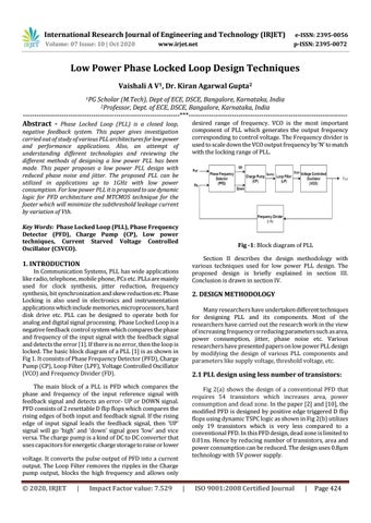
Fig -1: Block diagram of PLL Section II describes the design methodology with various techniques used for low power PLL design. The proposed design is briefly explained in section III. Conclusion is drawn in section IV.
1. INTRODUCTION In Communication Systems, PLL has wide applications like radio, telephone, mobile phone, PCs etc. PLLs are mainly used for clock synthesis, jitter reduction, frequency synthesis, bit synchronization and skew reduction etc. Phase Locking is also used in electronics and instrumentation applications which include memories, microprocessors, hard disk drive etc. PLL can be designed to operate both for analog and digital signal processing. Phase Locked Loop is a negative feedback control system which compares the phase and frequency of the input signal with the feedback signal and detects the error [1]. If there is no error, then the loop is locked. The basic block diagram of a PLL [1] is as shown in Fig 1. It consists of Phase Frequency Detector (PFD), Charge Pump (CP), Loop Filter (LPF), Voltage Controlled Oscillator (VCO) and Frequency Divider (FD).
2. DESIGN METHODOLOGY Many researchers have undertaken different techniques for designing PLL and its components. Most of the researchers have carried out the research work in the view of increasing frequency or reducing parameters such as area, power consumption, jitter, phase noise etc. Various researchers have presented papers on low power PLL design by modifying the design of various PLL components and parameters like supply voltage, threshold voltage, etc.
2.1 PLL design using less number of transistors:
The main block of a PLL is PFD which compares the phase and frequency of the input reference signal with feedback signal and detects an error- UP or DOWN signal. PFD consists of 2 resettable D flip flops which compares the rising edges of both input and feedback signal. If the rising edge of input signal leads the feedback signal, then ‘UP’ signal will go ‘high’ and ‘down’ signal goes ‘low’ and vice versa. The charge pump is a kind of DC to DC converter that uses capacitors for energetic charge storage to raise or lower
Fig 2(a) shows the design of a conventional PFD that requires 54 transistors which increases area, power consumption and dead zone. In the paper [2] and [10], the modified PFD is designed by positive edge triggered D flip flops using dynamic TSPC logic as shown in Fig 2(b) utilizes only 19 transistors which is very less compared to a conventional PFD. In this PFD design, dead zone is limited to 0.01ns. Hence by reducing number of transistors, area and power consumption can be reduced. The design uses 0.8µm technology with 5V power supply.
voltage. It converts the pulse output of PFD into a current output. The Loop Filter removes the ripples in the Charge pump output, blocks the high frequency and allows only
© 2020, IRJET
|
Impact Factor value: 7.529
|
ISO 9001:2008 Certified Journal
|
Page 424