International Research Journal of Engineering and Technology (IRJET)
e-ISSN: 2395-0056
Volume: 07 Issue: 10 | Oct 2020
p-ISSN: 2395-0072
www.irjet.net
An Efficient TCAM Design using Multicascading Technique Kevin Francis1, Nilima S. Warade2 1Student,
Dept. of Electronics and Telecommunication Engineering, AISSMS Institute of Information Technology, Maharashtra, India 2Professor, Dept. of Electronics and Telecommunication Engineering, AISSMS Institute of Information Technology, Maharashtra, India ---------------------------------------------------------------------***----------------------------------------------------------------------
Abstract - Ternary content-addressable memories are an
minimizing the transmission of faulty data wirelessly to cloud servers [3], [4]. FPGAs use SRAM to deploy TCAM by putting the content of the TCAM table into the SRAM block. Each specific TCAM pattern is represented by a single SRAM word, and the SRAM block stores the content of the entire data of the TCAM table. The increasing number of TCAM bits leads to a sharp increase in memory usage. The design mitigates this increase in memory usage by cascading many SRAM blocks.
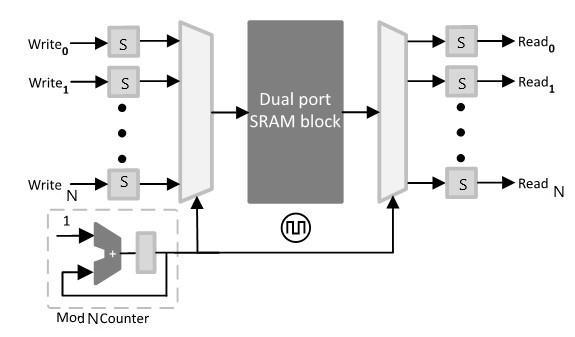
essential part of network routers. The space requirements of TCAM applications are increasing every day. Current solutions of TCAMs are affected by inefficiency in the storage space. The multicascading technique used for SRAM in this design achieves an effective storage use. Existing SRAM designs diminish the effect of the addition in the conventional TCAM pattern width from an sharp increase in memory utilization to a gradual one by using a cascaded configuration of block RAMs (BRAMs). But the BRAMs on the even the most advanced FPGAs have a limit in terms of minimum depth, which in turn affects the storage efficiency for the TCAM bits. Our proposed design circumvents this limit by mapping the divisions in the conventional TCAM table to sub blocks, which are not very deep. of the configured BRAMs, thus attaining an efficient memory design. The proposed design uses the configured two ported BRAMs of the design as a multiple port memory using the unique technique called as multicascading. This technique is implemented by clocking the block with a higher internal clock which is a multiple of the system clock, to access the various sub blocks of the block RAM in a single system cycle. Our design implemented in Xilinx ISE achieves better memory utilization, lower delay as well as lower power consumption with the increase in memory implementation size.
A summary of the main contributions of this paper is presented in the following. 1) A unique technique called multicascading which results in more efficient utilization of memory. 2) The proposed design presents a TCAM that is modular and highly scalable. 3) The reduction in routing due to using a smaller amount of BRAMs leads to the design being very practical for high storage capacity. The unique optimization methods of cascading the blocks of SRAM in the design reduces the general complexity of the AND operations. The proposed design is implemented using Xilinx ISE. A comparison of the proposed design and current designs is provided with respect to memory usage and other parameters. The proposed design results in up to 2 times better memory utilization.
Key Words: Field-programmable gate array (FPGA), memory architecture, static random-access memory (SRAM)-based ternary content-addressable memory (TCAM)
2. MATERIALS AND METHODS
1. INTRODUCTION
In recent times, memory is one of the most important features for the storage and retrieval of data. However, a large portion of device is used for data transmission memory in recent devices [5], [6], therefore TCAMs are used to mitigate this issue. In the current types of TCAM design have a limitation in terms of the minimum depth of the block RAM, which severely reduces the storage efficiency of the ternary CAM bits. Our proposed design will mitigate this issue by mapping the current TCAM design method to an SRAM with the unique technique of multicascading, which configures or arranges a number of sub blocks in one TCAM with the simple two port configuration. Here, this paper will present a multicascaded two port SRAM design in different limitations such as Case I = 512x28 (N=4), Case II = 512x32 (N=2), Case III = 1024x140 (N=4), Case IV = 2048x280 (N=4). This work will be implemented in Xilinx ISE using Verilog HDL and theoretically prove the better performance in terms of area, delay and power.
Ternary content addressable memory (TCAM) collates an input word parallelly with the data stored in the entire memory, and presents the result as the address of the word which was matched. TCAM accumulates the data in three states instead of the standard two: 0, 1, and X (which is the “don’t care” state). Conventional TCAMs are constructed by default in application specific integrated circuits (ASICs), and these provide fast search performance in a deterministic period. TCAM is commonly used in the design of high performance search algorithms and it has several applications in various fields such as networking, AI, information compression, signal detection, pattern recognition, image processing, and to increase the search performance of various primitives in a given database [1], [2]. Many IoT and big data analysis devices use TCAM in the form of a filter to store signature patterns, and also ti accomplish a significant increase in power efficiency by
© 2020, IRJET
|
Impact Factor value: 7.529
|
ISO 9001:2008 Certified Journal
|
Page 1683