6 minute read
MATERIALS AND METHODS


Volume: 07 Issue: 10 | Oct 2020 www.irjet.net p-ISSN: 2395-0072
Table -1: List of used notations.
Advertisement
Notation
Log2(SD) N
SD/N P Q Description Conventional TCAM Depth Conventional TCAM Width Configured Memory Depth Configured Memory Width Memory Block Address Bits Sub Blocks in Memory Block/ Multicascading factor Sub Block Depth TCAM MemoryRows TCAM Memory Columns
2.1 Multicascaded N Port SRAM
This unique technique called multicascading is used to multiply or increase the ports of a two port SRAM block by a factor N. This is carried out by multiplying the internal clock of the SRAM block to the same factor N of the external clock [7], [8], [9], [10].As shown in Figure 1 below, the two sides of the SRAM block are using a N to 1 multiplexer to address N read and write lines. The two lines are given access to the two port SRAM block in a circular method using the mod N counter bits.
Fig -1: Multicascaded N port memory: the SRAM block is clocked at an N multiple of system clock, enabling N access during a single external clock cycle.
2.3 Proposed Division of Conventional Table
2.2 Fundamental Idea
In this proposed design, thewidth of the memory is decided by how deep the conventional TCAM table is and hence the width of the conventional table is coded as the address of the memory block.
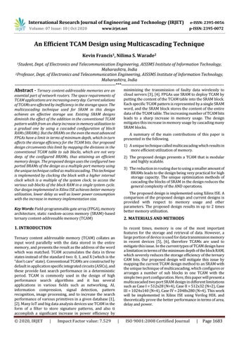
Figure 2 shows the basic concept of the proposed design which achieves an increase in memory efficiency. Figure 2(a) depicts a D = 1, W =8 conventional TCAM table, and Figure 2(b) depicts the implementation of the four TCAM bits by utilizing a D = 16,W =1 memory block.Figure 2(c) depicts the implementation of six bits by using a D = 16, W = 1 memory block, which has been multicascaded twice, each memory sub block having a size of Q = 8, P = 1 which emulates three bits. Figure 2(d) depicts the implementation of eight bits by using a D = 16, W=1 memory block, which has been multicascaded quadruple times, with each memory sub block having a of size Q= 4, P= 1 which emulates two bits. Thus, higher memory utilization efficiency (lesser physical memory bits are used for every TCAM bit) is achieved by using the unique technique of multicascadingas depicted in Figure 2(c) and 2(d) as compared to the design which does not utilize multicascading as depicted in Figure 2(b). Thus, the storage capacity of the memory block for the TCAM bits increases with the technique of multicascading.
A N ported memory block of size SD × SW with a multicascading factor of N implements a conventional table of size Nlog2(SD/N) × SW , each memory sub block of size (SD/N) × SW which emulates log2(SD/N) × SW table data, as depicted in Figure 3 and 1. Our proposed design achieves an increase in the table bits packing capacity with an rise in the multicascading factorN.
N.
Fig -2: (a) A conventional TCAM of P= 1,Q =8; (b) D = 16, W= 1 memory block without multicascading technique emulating P=1, Q= 4 table; (c)D= 16, W = 1 memory block with a multicascading factor of N= 2 emulating P = 1, Q =6 table; (d)D = 16,W= 1 memory block with a multicascading factor of N = 4 emulating P= 1,Q= 8 table.
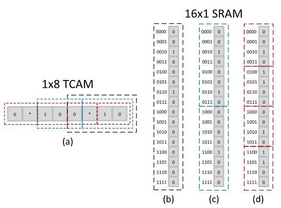
The conventional TCAM table which is sized D x W is divided into P x Q partitions, such that every partition has N parts of log2(SD/N) x SW size as shown in Figure 3. Our proposed design uses its configured memory blocks of SD ×SW size as N ported SRAM, having N sub blocks of size (SD/N) × SW as depicted in Figure 3.
Volume: 07 Issue: 10 | Oct 2020 www.irjet.net p-ISSN: 2395-0072
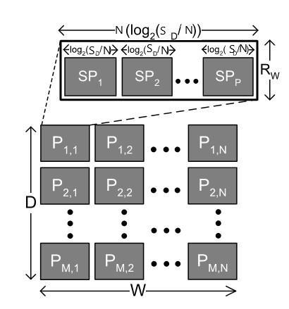
Fig -3: Proposed divisionof the conventionalTCAM table.
Every sub block of the memory stores log2(SD/N) × SW size divisions of the conventional TCAM. Accordingly, the N sub blocks of the N ported memory in our proposeddesign stores a conventional TCAM division of size Nlog2(SD/N) × SW as depicted in the Figures 3 and 1. Similarly, the P × Q divisions of size Nlog2(SD/N) × SW are mapped to the memory blocks of the P × Q TCAM memory units in the proposed design, as depicted in Figures 3 and 2.
2.4 Basic Architecture of Proposed Memory Design
The basic architecture of our proposed memory design is represented in Figure 4. The memory is connected by two clock signals -Sck that is the system clock, and Nck that is the internal clock of the memory block, both of which are synchronized. Nckis configured such that it is N times faster than Sck. The system clock Sck is used when an inbound TCAM bit is written in the shift register of bit length Y. The log2N counter shown in Figure 1 generates a log2N-bit number sequence within N cycles. This counter increases over the N clocks and is set to zero when it is reset. The log2N-bits produced by the counter are joined at the end with the log2(SD/N) bits from the shift register. Thissequence of bits makes the log2SD-bit address space of the physical memory.
During the positive edge of Nck, the log2N counter bits points to the beginning of the matching sub block and the shift register’s lower log2(SD/N) bits chooses the word in the sub block. In the Nck cycle, the memory words are ANDed and then accumulated in SY-bit register. The word lookup for the Y-bit input word is accomplished in N clock cycles by first reading it via the input line, then ANDing and subsequently accumulating the memory words from every memory sub block. Therefore, the N words in memory which have been ANDed and accumulated are presented as the matched word using Sck.
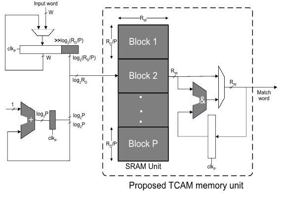
Fig -4: Basic architecture of the proposed memory design.
2.5 Modular Memory Design
The design of high storage capacity memory designs is realized by P x Q cascading units as depicted in Figure 5. The input W-bit memory word is split into P sub words consisting of Nlog2(SD/N) bits with the range of the bits represented in Figure 5. During the Sckcycle, the resulting sub words are kept in the P shift registers which are of size Nlog2(SD/N) bits. The N shift registers consisting of log2SDdirectories are used for parallely matching P memory units of the Q columns of the design using Nck cycle. The matched SY-bit words from every row of memory units are ANDed bit wise on Sck. Subsequently, the result of the ANDing operation are given to the accompanying priority encoder. Thus, the matched log2P bit address and the resulting information from each encoder unit are given to the global priority encoder unit that performs the task of outputting the match address according to the priority. The proposed memory design catalogues the input word and outputs a matched word in the Sck cycle. The memory unit updates the word in physical memory parallelly. The proposed design has the update latency of SD/N in the worst case scenario.
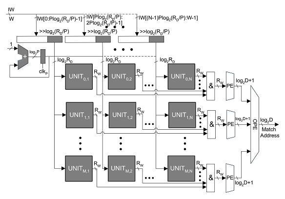
Fig -5: Grouping of the proposed high capacity memory units: (IW: input word, PE: priority encoder, GPE: global priority encoder).