International Research Journal of Engineering and Technology (IRJET) Volume: 05 Issue: 12 | Dec 2018 www.irjet.net
e-ISSN: 2395-0056 p-ISSN: 2395-0072
Implementation of Combined SVL Technique in Domino Inverter using Microwind K. Kalai Selvi Assistant Professor, Dept. of Electronics & Communication Engineering, Government College of Engineering, Tirunelveli, India ---------------------------------------------------------------------***---------------------------------------------------------------------
Abstract - This paper implements self controllable voltage
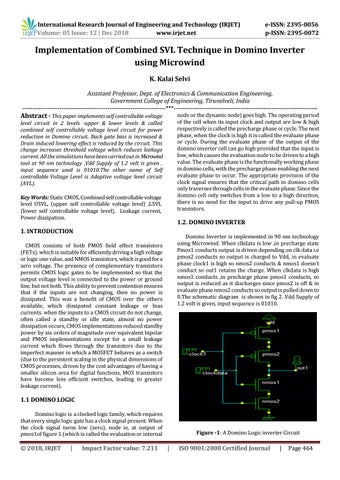
node or the dynamic node) goes high. The operating period of the cell when its input clock and output are low & high respectively is called the precharge phase or cycle. The next phase, when the clock is high it is called the evaluate phase or cycle. During the evaluate phase of the output of the domino inverter cell can go high provided that the input is low, which causes the evaluation node to be driven to a high value. The evaluate phase is the functionally working phase in domino cells, with the precharge phase enabling the next evaluate phase to occur. The appropriate provision of the clock signal ensures that the critical path in domino cells only traverses through cells in the evaluate phase. Since the domino cell only switches from a low to a high direction, there is no need for the input to drive any pull-up PMOS transistors.
level circuit in 2 levels -upper & lower levels & called combined self controllable voltage level circuit for power reduction in Domino circuit. Back gate bias is increased & Drain induced lowering effect is reduced by the circuit. This change increases threshold voltage which reduces leakage current. All the simulations have been carried out in Microwind tool at 90 nm technology ,Vdd Supply of 1.2 volt is given , input sequence used is 01010.The other name of Self controllable Voltage Level is Adaptive voltage level circuit (AVL). Key Words: Static CMOS, Combined self controllable voltage level USVL, (upper self controllable voltage level) ,LSVL (lower self controllable voltage level), Leakage current, Power dissipation.
1.2. DOMINO INVERTER
1. INTRODUCTION
Domino Inverter is implemented in 90 nm technology using Microwind. When clkdata is low ,in precharge state Pmos1 conducts output is driven depending on clk data i.e pmos2 conducts so output is charged to Vdd, in evaluate phase clock1 is high so nmos2 conducts & nmos1 doesn’t conduct so out1 retains the charge. When clkdata is high nmos1 conducts ,in precharge phase pmos1 conducts, so output is reduced as it discharges since pmos2 is off & in evaluate phase nmos2 conducts so output is pulled down to 0.The schematic diagram is shown in fig 2 .Vdd Supply of 1.2 volt is given, input sequence is 01010.
CMOS consists of both PMOS field effect transistors (FETs), which is suitable for efficiently driving a high voltage or logic one value, and NMOS transistors, which is good for a zero voltage. The presence of complementary transistors permits CMOS logic gates to be implemented so that the output voltage level is connected to the power or ground line, but not both. This ability to prevent contention ensures that if the inputs are not changing, then no power is dissipated. This was a benefit of CMOS over the others available, which dissipated constant leakage or bias currents. when the inputs to a CMOS circuit do not change, often called a standby or idle state, almost no power dissipation occurs, CMOS implementations reduced standby power by six orders of magnitude over equivalent bipolar and PMOS implementations except for a small leakage current which flows through the transistors due to the imperfect manner in which a MOSFET behaves as a switch (due to the persistent scaling in the physical dimensions of CMOS processes, driven by the cost advantages of having a smaller silicon area for digital functions, MOS transistors have become less efficient switches, leading to greater leakage current).
1.1 DOMINO LOGIC Domino logic is a clocked logic family, which requires that every single logic gate has a clock signal present. When the clock signal turns low (zero), node ie, at output of pmos1of figure 1 (which is called the evaluation or internal
Š 2018, IRJET
|
Impact Factor value: 7.211
Figure -1: A Domino Logic inverter Circuit
|
ISO 9001:2008 Certified Journal
|
Page 464