International Research Journal of Engineering and Technology (IRJET)
e-ISSN: 2395-0056
Volume: 05 Issue: 11 | Nov 2018
p-ISSN: 2395-0072
www.irjet.net
Comparison of Power Dissipation in inverter using SVL Techniques K. Kalai Selvi Assistant Professor, Dept. of Electronics & Communication Engineering, Government College of Engineering, Tirunelveli, India ---------------------------------------------------------------------***---------------------------------------------------------------------Abstract - As technology scales the size of chip, leakage power has become a important component in chip design. Leakage power is an essential parameter to be taken into account while designing low power devices .Large amount of leakage power is an serious & undesirable factor in portable electronics devices. High power consumption raises the cost and also reduces the battery life of the devices. So it is essential to reduce the dynamic as well as the static power consumption. Increasing the threshold voltage reduces the leakage power of the circuit. Low energy consumption in devices requires very low power circuits. This paper compares the inverter circuits i.e static CMOS inverter & Domino inverter with Upper & lower Self controllable Voltage Level (SVL). Power Consumption & power Dissipation of Upper SVL Domino circuit is found to be less . As power dissipation is reduced , consequently there must be a reduction in leakage power. All the simulations have been carried out in Microwind tool at 90 nm technology ,Vdd Supply of 1.2 volt is given , input sequence used is 01010.The other name of Self controllable Voltage Level is Adaptive voltage level circuit (AVL).
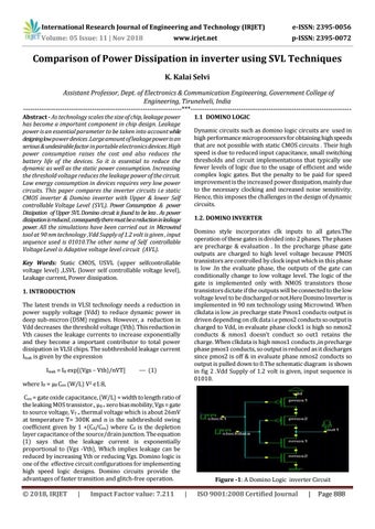
1.1 DOMINO LOGIC Dynamic circuits such as domino logic circuits are used in high performance microprocessors for obtaining high speeds that are not possible with static CMOS circuits . Their high speed is due to reduced input capacitance, small switching thresholds and circuit implementations that typically use fewer levels of logic due to the usage of efficient and wide complex logic gates. But the penalty to be paid for speed improvement is the increased power dissipation, mainly due to the necessary clocking and increased noise sensitivity. Hence, this imposes the challenges in the design of dynamic circuits. 1.2. DOMINO INVERTER Domino style incorporates clk inputs to all gates.The operation of these gates is divided into 2 phases. The phases are precharge & evaluation . In the precharge phase gate outputs are charged to high level voltage because PMOS transistors are controlled by clock input which in this phase is low .In the evaluate phase, the outputs of the gate can conditionally change to low voltage level. The logic of the gate is implemented only with NMOS transistors those transistors dictate if the outputs will be connected to the low voltage level to be discharged or not.Here Domino Inverter is implemented in 90 nm technology using Microwind. When clkdata is low ,in precharge state Pmos1 conducts output is driven depending on clk data i.e pmos2 conducts so output is charged to Vdd, in evaluate phase clock1 is high so nmos2 conducts & nmos1 doesn’t conduct so out1 retains the charge. When clkdata is high nmos1 conducts ,in precharge phase pmos1 conducts, so output is reduced as it discharges since pmos2 is off & in evaluate phase nmos2 conducts so output is pulled down to 0.The schematic diagram is shown in fig 2 .Vdd Supply of 1.2 volt is given, input sequence is 01010.
Key Words: Static CMOS, USVL (upper selfcontrollable voltage level) ,LSVL (lower self controllable voltage level), Leakage current, Power dissipation. 1. INTRODUCTION The latest trends in VLSI technology needs a reduction in power supply voltage (Vdd) to reduce dynamic power in deep sub-micron (DSM) regimes. However, a reduction in Vdd decreases the threshold voltage (Vth). This reduction in Vth causes the leakage currents to increase exponentially and they become a important contributor to total power dissipation in VLSI chips. The subthreshold leakage current Ileak is given by the expression Ileak = I0 exp[(Vgs – Vth)/nVT]
--- (1)
where I0 = μ0 Cox (W/L) V2 e1.8, Cox = gate oxide capacitance, (W/L) = width to length ratio of the leaking MOS transistor., μ0 = zero bias mobility, Vgs = gate to source voltage, VT = thermal voltage which is about 26mV at temperature T= 300K and n is the subthreshold swing coefficient given by 1 +(Cd/Cox) where Cd is the depletion layer capacitance of the source/drain junction. The equation (1) says that the leakage current is exponentially proportional to (Vgs -Vth), Which implies leakage can be reduced by increasing Vth or reducing Vgs. Domino logic is one of the effective circuit configurations for implementing high speed logic designs. Domino circuits provide the advantages of faster transition and glitch-free operation.
© 2018, IRJET
|
Impact Factor value: 7.211
Figure -1: A Domino Logic inverter Circuit
|
ISO 9001:2008 Certified Journal
|
Page 888