
International Research Journal of Engineering and Technology (IRJET) e-ISSN: 2395-0056
Volume: 11 Issue: 08 | Aug 2024 www.irjet.net p-ISSN: 2395-0072


International Research Journal of Engineering and Technology (IRJET) e-ISSN: 2395-0056
Volume: 11 Issue: 08 | Aug 2024 www.irjet.net p-ISSN: 2395-0072
Tan Chun Fui1 , Ajay Kumar Singh2
1 Senior Lecturer, Faculty of Information Science Technology, Multimedia University-Jalan Ayer Keroh Lama, Melaka, Malaysia
2 Professor, Electronics and Communication Engineering NIIT University, Alwar, Rajasthan India
Abstract - Tofulfilltheperformancedemandsoflow-power mobile devices,ahighION/IOFFratioatlow-VDDnecessitates aspecific devicedesign.TFETsareincreasinglyfavoreddueto their superior characteristics like low subthreshold slope and high transconductance compared to MOSFETs. However, silicon-based TFETs exhibit a drawback of low on-state current, limiting their applicability in high-performance scenarios. To address this issue, employing a narrower band gap material such as Ge can enhance tunneling efficiency at thesourceside.Furthermore, mitigatingthelargerambipolar currentassociatedwithSi-TFETscanbeachievedthroughanchannel hetero-gate-dielectric (HGD) TFET. This research aims to propose and characterize a novel TFET structure leveraging hetero structure and hetero-gate-dielectric advantages, thereby enhancing ION while suppressing ambipolar current. The structure incorporates a heterodielectric BuriedOxide(BOX) onthedopedsubstratetoreduce ambipolar current. The source-to-gate overlap technique is employed to attain the desired subthreshold slope (SS). All simulations are conducted using a 2-D TCAD simulator, specifically Atlas Silvaco. The structure is optimized based on metrics such as ION/IOFF ratio, and simulation results are compared with existing structures in literature for performance evaluation.
Key Words: TFET, Heterro Gate Dielectric, Ambipolar current,ONcurrent,simulation.
Previously,MOSFETminiaturizationwaseffectiveforcircuit performance enhancement, but in the post-scaling era, its effectivenessishinderedbyincreasedleakagecurrentand short channel effects (SCEs) [1-3]. To address these challenges,researchershaveproposedvariousalternative structures beyond planar ones [4-6], including multi-gate devicesandthoseemployingdifferentmaterialstoreplace standardCMOStechnology[7-9].Leakagecurrentemerges as a significant issue in the nanoscale regime, disrupting device stability. Thus, controlling leakage current without compromising ON current becomes a critical challenge. Nanowire transistors, particularly tunnel field-effect transistors (TFETs), have been suggested as potential replacements for planar MOSFETs [10-14]. Formerly, downsizing MOSFETs effectively boosted circuit
performance, but in the post-scaling era, short channel effects (SCEs) and increased leakage current have undermineditsefficacy[2-3].Variousnon-planarstructures, includingmulti-gatedevicesandalternativestoconventional CMOS technology, have been proposed in literature [4-9]. SuppressionofleakagecurrentwithoutcompromisingON currentisaprimarychallengeinthenanoscaleera,where leakage current significantly impacts device stability. Nanowire transistors, particularly tunnel field-effect transistors(TFETs),havebeensuggestedtomanageleakage current[7,10,15].
TFETsarepoisedtoreplaceplanarMOSFETsinthefuture [13,16,17].DespiteTFETsexhibitingareducedsubthreshold slope(SS)atroomtemperature(60mV/decade),theysuffer from two main drawbacks: lower ON current and higher ambipolarcurrent[14-18].TFETswithgate-drainoverlap structurehavebeenproposedtoreduceambipolarcurrent [9], albeit at the expense of reduced chip density. The ON currentofTFETdevicescanbeenhancedbyemployinghighk dielectric materials as gate insulators [18], albeit with increasedambipolarcurrent.Inaddressingthesedrawbacks, hetero-dielectricgate(HDG)TFETshavebeenproposedin literature.HDGTFETsutilizeSiO2atthedraintodecrease ambipolarcurrentandahigh-kmaterialpartiallynearthe sourcetoboostONcurrent.
Inthispaper,wehavestudiedtheelectricalbehaviourofthe n-channelHGDTFETdevicesintermsofsurfacepotential, tunnelingwidth,draincurrentandambipolarcurrent.We haveignoredthesource/draindepletionwidthduetoheavy dopingandquantumconfinementeffectduetosiliconfilm thickness(>3nm).Thestructureofthispaperisgiven as follows:Section2describesdevicestructureofthemodel. Section3discussestheelectricalbehaviouroftheproposed structureandattheend,weconcludethepaperinsection4
The2-Dstructureandcoordinatesystemoftheproposed n-channelhetero-gate-dielectricTFET(HGDTFET)isshown inFigure1below

International Research Journal of Engineering and Technology (IRJET) e-ISSN: 2395-0056
Volume: 11 Issue: 08 | Aug 2024 www.irjet.net p-ISSN: 2395-0072

Theproposedstructurehasahetero-dielectricgate,which meansthatthegatedielectriciscomposedoftwodifferent materials with different dielectric constants. The heterodielectricgateconsistsofaburiedoxidelayer(BOX)anda topdielectriclayer,whicharelocatedbetweenthemetalgate andthelow-k dielectriclayer.Thehetero-dielectricgateis designedtoreducetheambipolarcurrentandenhancethe on-statecurrentofthedevice
Thepseudo-2DmethodwasemployedtosolvethePoisson equationduetoitscomputationalefficiency,simplifyingthe solutionprocess.
ReferringtoFigure1,afterdisregardingfixedcarrieroxide charges, the 2-D Poisson's equation for the potential distributionψj(x,y)inthecorrespondingregionisexpressed as[19-20];

Where, Na is the channel doping concentration, j=1, 2 representstheregionIandregionIIrespectively,εsi isthe siliconpermittivity,ψj(x,y)isthe2-Delectrostaticpotential in the region I and II measured with respect to Fermi potentialrespectively.
The 2-D electrostatic potential in the channel can be represented as follows by assuming a parabolic potential profilealongthefilmthickness(i.e.alongthey-direction),

Where, , and areconstantsandfunctionof xonly.ThefollowingBoundaryConditions(BCs)canbeused toobtaintheseconstants:


Where issurfacepotential, isflat-bandvoltagewhichisgivenas


The proposed analytical models are simulated for following values of the parameters; L=50 nm, tox1=tox2=3 nm, tsi=10 nm, Vds=0.7V,Ns=1020/cm3,Nd=1018 /cm3,Nc=1016 /cm3 unlessand until specified
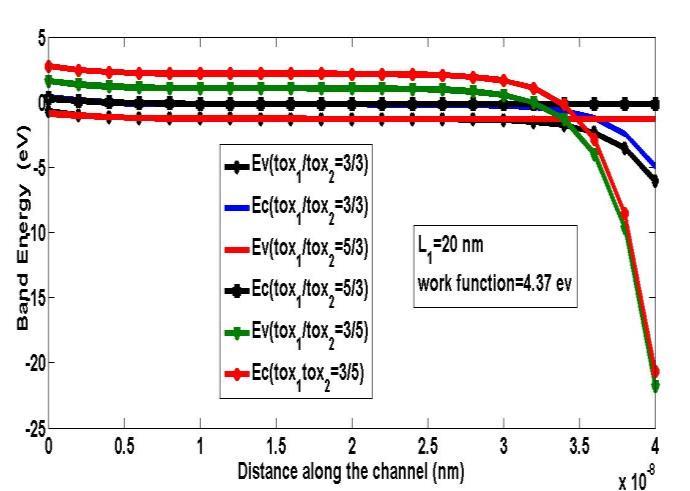
Fig -2:Banddiagramforvariouscombinationofoxide thicknessesintworegions
From Figure 2 above, the result shows that sharp band bendingoccursfortox1=3nmandtox2=5nmduetoreduction ofequivalentoxidethicknesswhichenhancesthecoupling between the gate and the channel junction. The surface potentialchangewasobservedtooccurmainlywithin about 10nmfromthesource-channelinterface.Thisisentirelyin the high-k region. The surface potential outside the tunnelingspace(mainlyinthelow-kregion)changeslittle. This indicates that the tunneling is controlled only by the high-kdielectricandthedrainhasnoeffectonthetunneling current. This behavior allows for better control and optimizationofthetunnelingcurrent,leadingtoimproved transistor performance. By focusing on optimizing the propertiesofthehigh-kdielectric,suchasitsthicknessand dielectric constant, the TFET can be designed to achieve specific performance targets such as low power consumption,highspeed,orhighgain.
Figure3showsthevariationofsurfacepotentialalongthe channeloftheproposedstructure.Thesurfacepotentialfirst reducesalongthechannelforx≤25nmandthenincreases sharply. The sharp rise in surface potential near drain

International Research Journal of Engineering and Technology (IRJET) e-ISSN: 2395-0056
Volume: 11 Issue: 08 | Aug 2024 www.irjet.net p-ISSN: 2395-0072
restricts the tunnel of carriers from drain to channel and hence suppresses the ambipolar current. The change in surface potential due to increased gate-source voltage greatlynarrowsthetunnelingwidthforchargecarriersnear sourceandhenceresultsinlargertunnelingprobability.The MAPE (mean absolute percentage error) reported in betweenmodeland2-DsimulatorresultsaregiveninTable 1. The error between two results is less than 5% which confirmsthevalidityofthedevelopedanalyticalmodel.

-3:Surfacepotentialvariationalongchannellength: comparisonwith2-DATLASsimulator
Table -1: MeanAbsolutePercentageError(MAPE)
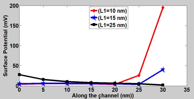
-4:Surfacepotentialvariationalongchannellengthfor differentlengthofHigh-κOxide
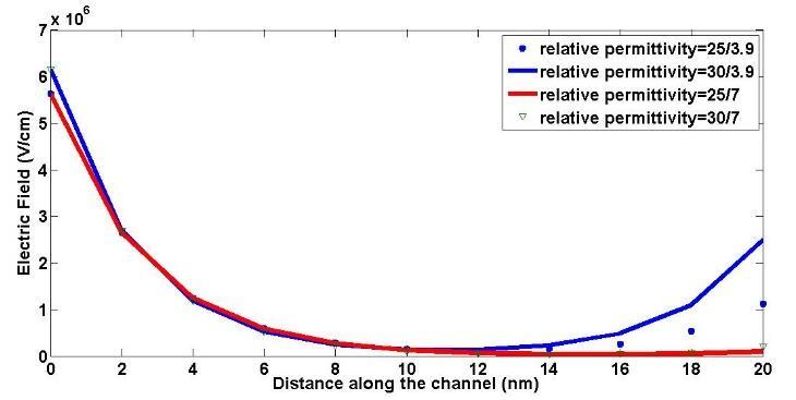
Fig -5:Variationoftheelectricfieldalongthechannelfor differentdielectricconstant(relativepermittivity) combinations
The effect of length L1 on the surface potential of the proposed structure has been analyzed. As L1 decreases, conductionbandbecomesshallowerwhichresultsinlower tunneling currents whereas the increase in L1 results in wider conduction band as seen from Figure 4. The larger conductionbandincreasestheambipolarcurrent.Therefore, torestricttheambipolarcurrentand toachievelargerON currentwehavechosenL1=15nmwhichisthebestchoice. Thischoiceoffersagoodbalancebetweenthetwoimportant characteristics of TFETs namely, tunneling and ambipolar currents
The lateral electric field decreases along the channel and reachesaminimumvalueinmid-rangeofthechannel.Figure 5showsthevariationoftheelectricfiledalongthechannel for different combinations of dielectric constants. We observed that electric field takes on a larger value when regionIisoccupiedbyhigh-kdielectricmaterial.
ThelateralaswellastransverseelectricfieldofregionIIhave beenanalyzedindetailasshowninFigure6.Boththefields increase as the dielectric constant κ-increases. From analytical results, it is observed that for κ≤ 4, fields take negative value. The negative field in drain-channel region deceleratesthecarriersandhencesuppressestheambipolar current. From this result, it is clear that SiO2 dielectric materialneardrain-channelregion,isthenaturalchoiceto controltheambipolarcurrent

International Research Journal of Engineering and Technology (IRJET) e-ISSN: 2395-0056
Volume: 11 Issue: 08 | Aug 2024 www.irjet.net p-ISSN: 2395-0072

-6:ElectricFieldVariationwithdielectricconstantin regionII
Figure7showsthevariationoflateralelectricfieldinregion IalongthechannelforsingledielectricgateTFETandhetero dielectricgateTFETwhenκ=25andκ=50.Itisobservedthat field takes larger value near source-channel junction for κ=50duetobettercontrolofgateoverthechannel.Thepeak ofthelateralelectricfieldnearthesource-channelinterface isresponsibleforthelargertunnelingprobability.
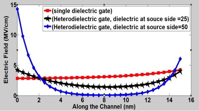
Fig -7:TotalElectricFieldvariationalongregionIfor singledielectricgateandHetero-dielectricgate
Increasing the doping concentration ratio between the source and drain regions leads to a more abrupt surface potential near the source end, resulting in improved electrical characteristics characterized by a narrower tunneling width. This effect consequently lowers the threshold voltage independent of the channel length, as depictedinFigure8.

Fig -8:ThresholdVoltageofHGDTFETDeviceVersus ChannelLengthforDifferentConcentrationsCombination intheSourceandDrainRegions
As the length of region 1 decreases, conduction band becomes flatten, which makes band-to-band tunneling difficultandhenceincreasesthethresholdvoltage.Thisis duetotheconductionbandbecomesmoreflat,whichmakes itharderforband-to-bandtunnelingtooccur,asshownin Figure9. ItisobservedthatthelargertunnelinglengthL1 accumulates more charges, which resulting in a lower thresholdvoltage.

Fig -9:ThresholdVoltageVariationwithtox forDifferent TunnelingLength(L1)
Figure 10 shows the variation of drain current per unit channel width with gate source voltage. For negative gate bias voltage, ambipolar current decreases and reaches its minimum value at Vgs= -0.4 V. The on-current starts only whengate-sourcevoltageisequalorlargerthanthreshold voltage which is more than 500 mV in this structure. The meanabsolutepercentageerror(MAPE)iscalculatedinthis caseandfoundtobe3.1%whichconfirmsthevalidityofthe developedanalyticalmodelofcurrent.Theslightdifference atlowergatesourcevoltageisduetonegligenceofmobile carriers.

International Research Journal of Engineering and Technology (IRJET) e-ISSN: 2395-0056
Volume: 11 Issue: 08 | Aug 2024 www.irjet.net p-ISSN: 2395-0072
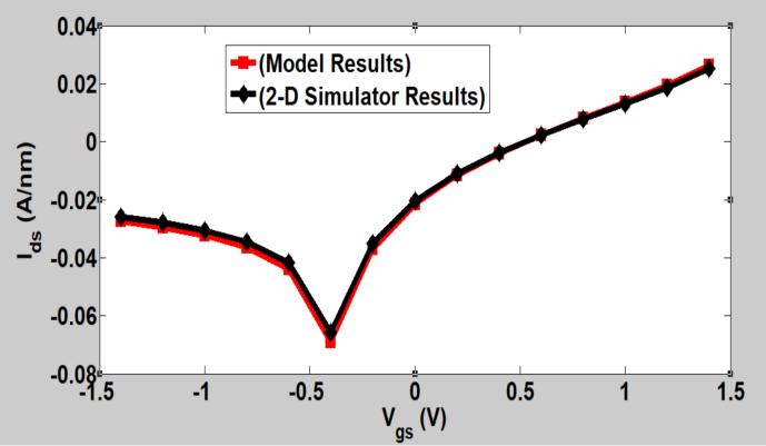
-10:Comparisonofdraincurrentwith2-DATLAS simulatorresults
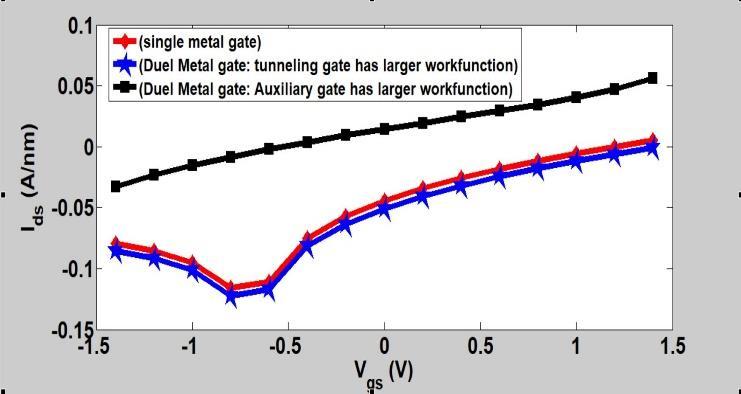
Toseetheeffectofworkfunctiononthedraincurrentofthe heterodielectricgateTFET,wehavestudiedthecurrentfor single metal TFET and dual metal TFET under two cases; cas11:tunnelgatehavinghigherworkfunction(4.5eV)than auxiliary gate (4.25 eV) and case 2: auxiliary gate having higher work function (4.5 eV) than tunnel gate (4.25 eV). Figure11showsthesimulationresults.Incase2,theband widthoverlapsincreasewhichresultsinnarrowtunneling widthandhenceultimatelyon-currentincreasesonthecost of increased ambipolar current. This result also suggests thattheworkfunctiondifferenceresultsinchangeinsurface potential which improves the gate control over tunneling process.Anarrowtunnelingwidthgivesalargertunneling probabilityofcarriers.Therefore,wecanconcludethatgate dielectric engineering along with choice of metal can be employed in HDG TFEET design to enhance the tunnel currentandreducetheambipolarcurrent.
:
4. CONCLUSIONS
ThispaperoffersacomprehensiveanalysisoftheHGDTFET device, a promising candidate for low-power and highperformanceapplications.Theproposedtunnelwidthmodel isvalidatedthrough2-DTCADsimulationresults,showing goodagreement.Thedevicestructureeffectivelysuppresses ambipolarcurrent,enhancesONcurrent,andmitigatesshort
channel effects. Gate engineering proves effective in reducing ambipolar current, increasing transconductance, andloweringthethresholdvoltage.Moreover,theproposed structure exhibits a lower subthreshold slope and higher transconductancecomparedtoconventionalTFETdevices. To further enhance device performance, a combination of materialengineeringandthinnersourcegateoxidecanbe employed.Overall,thispaperprovidesvaluableinsightsinto thedesignandoptimizationofHGDTFETsforfuturelowpowerandhigh-performanceelectronicapplications
[1] D'Agostino F, Quercia D. "Short-channel effects in MOSFETs",Proc.IntroductionVLSIDesign(EECS467), pp. 1-15, Dec. 2000.J. Clerk Maxwell, A Treatise on Electricity and Magnetism, Oxford: Clarendon, 1892; 2(3):68-73.
[2] A. Chaudhry, M. J. Kumar, "Controlling short-channel effectsindeepsubmicronSOIMOSFET'sforimproved reliability:Areview",IEEETrans.DeviceMater.Rel.,vol. 4,no.1,pp.99-109,Mar.2004
[3] M. Ali Pourghaderi, Anh-Tuan Pham, Hesameddin Hatikhameseh, Jongchol Kim, Hong-Hyun Park, Seonghoon Jin, Won-Young Chung, Woosung Choi, ShigenobuMaeda,Keun-HoLee,"UniversalityofShortChannelEffectsonUltrascaledMOSFETPerformance", IEEEElectronDeviceLetters,2018;39(2):168-171.
[4] .RiyadiMA,SusenoJE,IsmailR."Thefutureofno-planar nanoelectronicsMOSFETdevices:Arevies",J.Applied Science,2010;10:2136-2146
[5] D. Bhattacharya, NK. Jha, "FinFETs: From devices to architectures",Adv.Electronvol.2014;pp.1-21.
[6] Ravi Shankar Pal, Savitesh Sharma, Sudeb Dasgupta, "Recent trend of FinFET devices and its challenges: A review", 2017 Conference on Emerging devices and SmartSystems(ICEDSS).
[7] JP. Colinge, FinFETs and other Multi-Gate Transistors, NewYork,NY,USA:SpringerScience+BussinessMedia, 2008.
[8] SL.Tripathi,R.Mishra,RA.Mishra,"Multi-gateMOSFET structureswithhigh-kdielectricmaterials",J.Electron Devices2012;16:1388-1394.
[9] Jansung Park, Sung-Min Hong, "Simulation study of enhancement mode Multi-Gate vertical Gallium Oxide MOSFETs", ECS journal of Solid State Science and Technology2019;8(7):Q3116-Q3121.
[10] Lu W, Xie P, Lieber CM. "Nanowire transistor performance limits and applications", IEEE Trans. ElectronDevices2008;55(11):2859-2876.

International Research Journal of Engineering and Technology (IRJET) e-ISSN: 2395-0056
Volume: 11 Issue: 08 | Aug 2024 www.irjet.net p-ISSN: 2395-0072
[11] Su PC, Chen BH, Lee YC, Yang YS. "Silicon Nanowire Field-EffectTransistorasBiosensingPlatformsforPostTranslational Modification", Biosensors, 2020; 10: pp. 213.
[12] Chang SM, Palanisamy S, Wu TH, et al. " Utilization of siliconnanowirefield-effecttransistorsforthedetection of a cardiac biomarker, cardiac troponin I and their applicationsinvolvinganimalmodels",SciRep2020;10: pp.22027.
[13] ChoiWY,ParkBG,LeeJD,LiuTJK."Tunnelingfield-effect transistors(TFETs)withsubthresholdswing(SS)less than 60 mV/dec", IEEE Electron Device Lett 2007; 28(8):743-745.
[14] Priya GL, Venkatesh M, Balamurugan NB. et al. Triple MetalSurroundingGateJunctionlessTunnelFETBased 6T SRAM Design for Low Leakage Memory System. Silicon2021;13:1691-1702.
[15] J. Kim, H.-Ch. Lee, K.-H. Kim et al., "Photon-triggered nanowiretransistors",NatureNanotechnology,no.12, pp.963-968,2017.
[16] D. Nikonov, Tunneling fets, [online] Available: https://nanohub.org/resources/18351.
[17] M. Adrian, and Riel Heike, “Tunnel field-effect transistors as energy-efficient electronic switches”, Nature,Vol.479,pp.329-337,2011.
[18] H. Ilatikhameneh, T. A. Ameen, G. Klimeck, J. Appenzeller,R.Rahman,"Dielectricengineeredtunnel field-effect transistor",IEEE Electron DeviceLett.,vol. 36,no.10,pp.1097-1100,Oct.2015.
[19] AjayKumarSingh,TanChunFui,LimWaySoong,“Drain currentmodelforahetero-dielectricsinglegatetunnel field effect transistor (HDSG TFET)”, International Journal of Numerical Modelling Electronic Network, DevicesandFields,(IJNM),onlinepublished14thDec, 2021.
[20] Singh,A.K.,&Fui,T.C.(2021).DualMetalTriple-gatedielectric (DM_TGD) Tunnel Field Effect Transistor: A Novel Structure for Future Energy Efficient Device. RecentAdvancesinElectrical&ElectronicEngineering (Formerly Recent Patents on Electrical & Electronic Engineering),14(6),683-693.