
International Research Journal of Engineering and Technology (IRJET) e-ISSN: 2395-0056
Volume: 12 Issue: 01 | Jan 2025 www.irjet.net p-ISSN: 2395-0072

International Research Journal of Engineering and Technology (IRJET) e-ISSN: 2395-0056
Volume: 12 Issue: 01 | Jan 2025 www.irjet.net p-ISSN: 2395-0072
Atharva Suhas Kulkarni1 ,
1Electronics & Telecommunication
Abstract - Thedemandfor greatermemorycapacityinthe electronics industry, coupled with the limitations of existing memory technologies due to scaling challenges, has driven the exploration of next-generation memory solutions. Technology scaling often leads to reduced stability, increased leakage currents, and higher standby power dissipation in electronic circuits. To address these issues, spin-transfer torque random access memory (STT-RAM) emerges as a promising alternative, offering features such as non-volatility, zero standby leakage, rapid access times, high density, efficient read and write performance, and low powerusage. Thisstudyintroducesanon-volatilehybrid6T4MTJ SRAM bit cell utilizing 32-nanometer technology. It is benchmarked against a conventional 6T SRAM bit cell to analyse the impact of process, voltage, and temperature (PVT)variationsonkey designmetrics.Theproposedhybrid 6T-4MTJ bit cell demonstrates reduced write delay spread and significantly lower leakage power compared to standard CMOS-based SRAM cells. Additionally, the MTJbased SRAM design enhances overall stability by 19.49% while achieving a remarkable 92% reduction in power consumption.
Key Words: Magnetic Tunnel Junction (MTJ), MRAM, Spintronics, Non-volatile.
In 2023, the global Internet of Things (IoT) market generated $293.2 billion in revenue, a figure projected to triple to $621.6 billion by 2030. Among the critical components driving modern IoT-based technologies is electronic memory. Memory serves as a fundamental unit for storing data, including the instructions required for processing it. Memory is broadly categorized into two types: Random Access Memory (RAM) and Read-Only Memory(ROM).RAMisvolatile,meaningitlosesallstored datawhenthepowersupplyisinterruptedorswitchedoff. In contrast, ROM is non-volatile and retains its data even in the absence of a power supply. This distinction makes memoryanessentialelementinpoweringIoTapplications efficientlyandreliably.
Technologies such as CMOS (Complementary Metal Oxide Semiconductor), CNTFET (Carbon Nano Tube Field Effect Transistor), and FinFET (Fin-type Field Effect Transistor) play vital roles in enabling efficient data storage in memory. CMOS technology, widely used in
***
Engineer, Maharashtra, India
designing integrated circuits, combines complementary NMOS and PMOS semiconductors in MOSFETs to create a variety of logic gates. This technology offers several advantages over alternatives like TTL, RTL, and NMOS, including a high noise margin, low static power dissipation, fast switching speed, and thermal efficiency. However, despite these strengths, CMOS devices exhibit slower read and write operations due to the relatively slowswitchingspeedoftheirMOSFETcomponents.
In advanced integrated circuit (IC) designs at 32nm or smaller, CMOS technology has faced limitations such as increased power consumption and leakage current. To address these challenges, emerging technologies like CNTFET and FinFET have gained traction. These technologies provide enhanced control over the thin silicon body, offering improved performance metrics. CNTFETs,forinstance,simplifythemanufacturingprocess byutilizingrolled-uphollowcylindricalcarbonnanotubes. Theyalsoreducesourceanddrainwidth,leadingtobetter gate capacitance, faster switching speeds, and improved short-channel immunity. Furthermore, CNTFETs require less power and propagation delay compared to CMOS devices.
However, CNTFETs have limitations, including a lower on-off current ratio compared to traditional transistors, which can make accurate data read and write operations more difficult. Additionally, defects in carbon nanotubes can alter their electrical properties, reducing the number of usable nanotubes in a device and potentially hindering thescalabilityof CNTFET-basedcircuits. Thesechallenges can impact the reliability of CNTFETs in large-scale applications, particularly for critical operations like readingandwritingdata.
FinFETs feature a shorter channel length compared to CMOS transistors, enabling faster switching speeds and enhanced performance. Their larger effective channel widthalsosupportshigher drivecurrents,contributing to superior overall efficiency. However, the 3D architecture of FinFETs can increase the capacitance between the gate andthechannel,potentiallyreducingtheefficiencyofread and write operations. This higher capacitance may also lead to slower switching speeds and increased power consumption. Additionally, compared to traditional CMOS transistors, FinFETs come with higher manufacturing costs due to their greater structural complexity and

International Research Journal of Engineering and Technology (IRJET) e-ISSN: 2395-0056
Volume: 12 Issue: 01 | Jan 2025 www.irjet.net p-ISSN: 2395-0072
variability, which can make production processes more challenging.
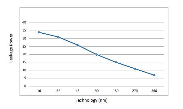
Chart -1:LeakagePowerAnalysis
As nanoscale technology continues to scale down, leakage power increases significantly (as illustrated in Chart-1), posing a major challenge due to the resulting higherpowerdissipationinelectroniccircuits.Thismakes further miniaturization of technology a complex and criticalobstacletoovercome[4].
Spintronics, or spin electronics, is a field of study that explores the electron's intrinsic spin and magnetic moment alongside its electrical charge in solid-state devices. This technology leverages the spin property of electrons, in addition to their charge, to enable functionality. The spin property, which refers to the intrinsic angular momentum of elementary particles like electrons,neutrons,protons,andneutrinos,playsacentral role in spintronics. Compared to traditional semiconductor devices, spintronic devices offer distinct advantages, such as non-volatility, greater scalability, and enhanced flexibility. The advancement of spintronics has been largely driven by the development of Magnetic TunnelJunction(MTJ)technology[5].
A Magnetic Tunnel Junction (MTJ) consists of two ferromagnetic layers, typically made of magnetic metals likecobalt-iron,separatedbyathininsulatingoxidelayer, such as magnesium oxide or aluminum oxide, with a thicknessofapproximately1nm.Thisultra-thininsulating layerallowselectronsto tunnel throughthe barrier when a bias voltage is applied across the two metal electrodes [6]. The tunneling current in MTJs is determined by the relative orientation of the magnetizations of the two ferromagnetic layers, which can be altered by an external magnetic field. MTJs offer several advantages, including excellent scalability, low power consumption, high-speed read and write operations, unlimited programming endurance,andenhancedscalability[7]
Thetunnelmagneticresistance(TMR)ratioisdefinedas the ratio of the two resistances in a Magnetic Tunnel
Junction (MTJ). Efforts are being made to improve the TMR ratio of MTJs to enable better integration with other devices.Forhybridcircuits,a TMR intherangeof50% to 200% is typically sufficient to differentiate the voltage levels corresponding to logic states "0" and "1." This capability makes MTJs versatile for various applications [8][9].
TMR=
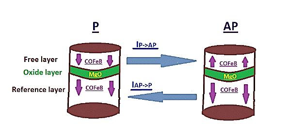
Binary bits in magnetic memory based on Magnetic Tunnel Junctions (MTJs) can be stored in two distinct modes: Antiparallel (AP) and Parallel (P), as illustrated in Fig-1
Fig
MTJs consist of layers with spinning electrons, where the direction of electron spin either clockwise or counterclockwise determines whether the device is in a Parallel or Antiparallel state. In these devices, one layer's orientationisfixedasareference,whiletheorientationof the other layer can be changed depending on the applied voltage.
Whentheorientationsof thetwolayersareopposite, a transition from parallel to antiparallel orientation occurs. Conversely, if the orientations are not opposed, a switch from antiparallel to parallel orientation is possible. The symmetry of the MTJ whether parallel or perpendicular depends on the materials used in its construction. Additionally, the insulating material on the drain side of the MTJ has a high melting point, which is crucial due to the significant power dissipation involved withthetransistorconnectedtotheMTJ'scollector[10].
The "1T-1MTJ" structure, whichincludes one transistor and one magnetic tunnel junction with a tunneling oxide layer sandwiched between two ferromagnetic layers, is a widely used cell structure in Spin-Transfer Torque Magnetoresistive Random-Access Memory (STT-MRAM), as depicted in Fig. No. 3. In this structure, the "Reference layer" (RL) has a fixed magnetization, while the "Free layer" (FL) can have one of two potential magnetization orientationstorepresentbinarydata.[11]

International Research Journal of Engineering and Technology (IRJET) e-ISSN: 2395-0056
Volume: 12 Issue: 01 | Jan 2025 www.irjet.net p-ISSN: 2395-0072
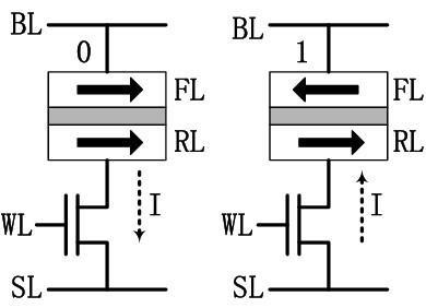
To write data to a Magnetic Tunnel Junction (MTJ), a current is passed through the transistor, generating a magnetic field that alters the magnetization orientation of thefreelayer.Thestoreddata’sstateisdeterminedbythe direction of this magnetization. To read the data, a small voltage is applied across the MTJ, and the resulting resistance is measured. This resistance is dependent on themagnetization'sorientationinthefreelayerandcanbe usedtodeterminethestoreddata'sstate[11]
Write Operation: To write data to an MTJ cell, currents flowing in opposite directions are used to set the cell to a "0"or"1"state.
Writing "0": The MTJ is set to a parallel state, with the word line (WL) and bit line (BL) connected to the supply voltage (VDD), and the source line (SL) grounded, as shown in Figure No. 3(a). The transistor can operate in either the saturation or linear region, depending on its width.
Writing "1": The MTJ is set to an anti-parallel state, with thewordline(WL)andsourceline(SL)connectedtoVDD, andthebitline(BL)grounded,asillustratedinFigureNo. 3(b). In this case, the transistor operates in its saturation region.
ReadOperation:Therearetwomethodstoreaddatafrom the cell: parallel (P) direction and anti-parallel (AP) direction.
ParallelReading(P): Averylowvoltageisappliedbetween the bit line (BL) and source line (SL) during parallel reading. Once the word line (WL) is activated, current flowsfromthebitline(BL)tothesourceline(SL).
Anti-Parallel Reading (AP): During anti-parallel reading, the polarity of the voltage applied to the bit line (BL) and sourceline(SL)isreversed.Asaresult,currentflowsfrom SLtoBLintheoppositedirection.
Fig -3 illustrates the schematic design of the proposed 6T-4MTJ Hybrid SRAM bit cell, which mirrors the structureofaconventional6T-SRAMcell.Thecellemploys
cross-coupled CMOS inverters (latch) to store the complementary electrical states (Q Q) of volatile data. Beyond the CMOS latch, the design incorporates two nonvolatileMRAMstatesintegratedinto the pull-upand pulldown networks of the latch. Each MRAM state contains two perpendicular STT-MTJs, which must maintain opposingstatestoensurepropercelloperation[12].
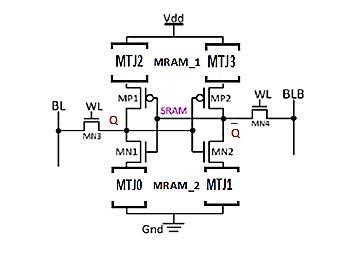
Fig -3: 6T-4MTJ
WriteOperation:
To write data into a T-4MTJ circuit a voltage pulse is applied to either Q or Q depending on the desired value. This pulse activates the transistor connected to the correspondingMTJ,enablingtheconnectionofthebitline (BL) or its complement (BLB) to the selected MTJ as determined by the state of Q or Q. If the selected MTJ exhibitslowresistance,thevoltageonthebitline(BL)will remain relatively unchanged, indicating that the correct data value is already stored in the MTJ. Conversely, if the MTJ has high resistance, the voltage on the bit line (BL) will vary significantly, signaling the need to flip the magnetizationoftheMTJtostorethedesiredvalue.
To achieve this magnetization flip, a voltage pulse is applied to the complementary bit line (BLB or BL). This generates a magnetic field sufficient to alter the magnetizationdirectionofoneoftheferromagneticlayers withintheMTJstack.Knownas“spintransfertorque”this process enables the magnetization direction to switch between parallel and anti-parallel states, effectively storingthenewdatavalue.
ReadOperation:
Readingdatafroma T-4MTJcircuitinvolvesapplyinga voltageto bothQandQ therebyactivatingthetransistors linked to all MTJs. The resistance of each MTJ is then measured using the bit lines BL and BLB, with the stored datainterpretedas0or1basedontheresistancevalues.

International Research Journal of Engineering and Technology (IRJET) e-ISSN: 2395-0056
Volume: 12 Issue: 01 | Jan 2025 www.irjet.net p-ISSN: 2395-0072
If the selected MTJ has low resistance, the corresponding bit line voltage will show minimal change, indicating a stored valueof0.However, iftheMTJhashighresistance, the bit line voltage will shift significantly, indicating a storedvalueof1.
PtoAP:Time-dependently,theMTJ'sresistancerisestoits maximumvalue,resultinginminimalcurrentflow.
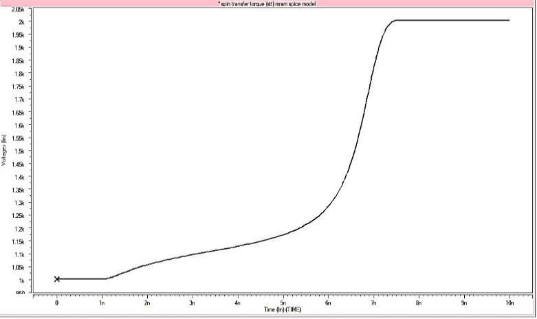
Fig -4: PtoAPresistanceanalysis(Write0)
AP to P: Time-dependently, 1T1MTJ's resistance is decreased to zero, allowing the maximum amount of currenttoflowthroughit.
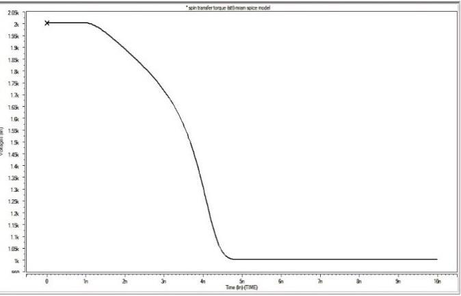
Fig -5: APtoPresistanceanalysis(Write1)
3.2 1T-1MTJ: Proposed MTJ-based Non-Volatile Hybrid 6T-4MTJ SRAM bit cell
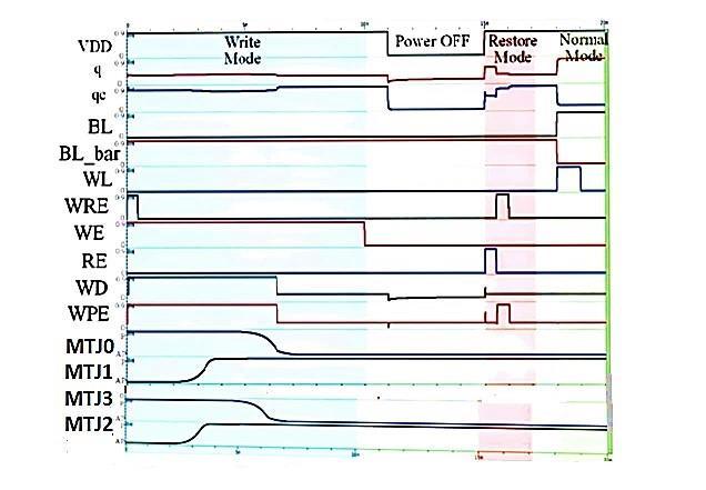
Fig -6: Simulationwaveformoftheproposednonvolatile 6T-4MTJSRAMbitcell
WriteOperationfortheProposed6T-4MTJCell:
The write operation for the proposed 6T-4MTJ cell is represented in the first region, highlighted in blue in Fig. No. 7. The initial states of MTJ1 and MTJ2 are assumed to be parallel, with MTJ1 starting in a low-resistance state (LRS) and MTJ2 in a high-resistance state (HRS). To store thevaluesq=0andqc=1,thestatesofbothMTJsmustbe flipped.
During the entire write operation, the Write Enable (WE)signalremainsactivewhensethigh.Additionally,the Write & Restore Enable (WRE) signal is pulsed with a duration of 1 ns to activate the transistor and initiate the write current. The voltage at the nodes q and qc determines the direction of the current flow through the MTJs.
The current flows from Vdd through MTJ2 and q, causing MTJ0 and MTJ3 to transition to a high-resistance state. Simultaneously, MTJ1 and MTJ2 are switched to a low-resistance state, successfully completing the write operation.[13]
3.3 1T-1MTJ: Overall Stability of Hybrid 6T-4MTJ SRAM bit cell
Thestaticnoisemargin(SNM)isameasureofthestability of SRAM circuits. There are two primary methods for determiningtheSNMofanSRAMcell:
Graphical Method: This approach involves plotting the inverted characteristics of the SRAM cell and identifying

International Research Journal of Engineering and Technology (IRJET) e-ISSN: 2395-0056
Volume: 12 Issue: 01 | Jan 2025 www.irjet.net p-ISSN: 2395-0072
the largest square that can be enclosed between the mirroredcurves.
Butterfly Curve Method: In this method, noise source voltages are applied to the nodes of the SRAM cell to generate a "butterfly curve" with two distinct lobes. The SNM is then calculated based on the largest square that canfitwithintheselobes.[14]
SNMCalculation:
The SNM is determined by finding the maximum side length of the square that fits within the butterfly curve's lobes.Mathematically,itisexpressedas:
SNM= √
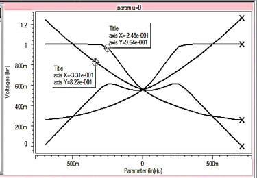
Fig -7: SNMcurveof6T-4MTJMRAMcell
Asa result,(Fig -7)showsthatcomparedtothe6T SRAM bitcell,theoverallstabilityhasimprovedby19.49%.
3.4 1T-1MTJ: Average power analysis of proposed 6T-4MTJ with standard 6T SRAM bit cell
TableNo. 1illustratesa comparisonoftheaveragepower consumption of 6T and 6T-4MTJ circuits. It is observed that the 6T circuit consumes significantly more power. Incorporating MTJs into the circuit substantially reduces the average power consumption. Based on the recorded data,itisestimatedthattheadditionofMTJscandecrease theaveragepowerconsumptionbyapproximately92%.
Table -1: Averagepowercomparisonbetween6Tand6T4MTJ
Power(for2.2Volts)
ReadAccessTimeorReadDelay
The read delay is defined as the time interval from the activationofthewordlinetothemomenttheoutputnode transitions- either rising for a "1" read or falling for a "0" read.The6T-4MTJcellimprovestheswitchingtimeofthe read operation, as it eliminates the need for additional voltage to initiate the cell, resulting in faster performance (Fig-7).
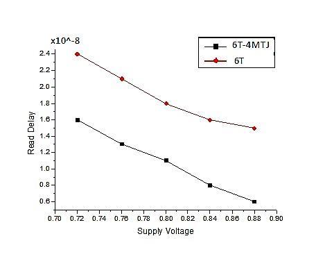
Fig -7: ReadDelayComparison
WriteAccessTimeorReadDelay
The write delay is defined as the time interval from the activation of the word line to the point when new data is writtentothebitcell nodes. Thedifferenceinwritedelay betweenthe10T(6T-4MTJ)andconventional6TSRAMbit cells is negligible, as the dimensions of the pull-up and access devices, which primarily dictate the write delay, remain identical in both configurations. However, the 6T4MTJ cell enhances the write operation speed due to its switching time, as it eliminates the need for an additional voltagetoactivatethecell(Fig.No.10).
Technology

International Research Journal of Engineering and Technology (IRJET) e-ISSN: 2395-0056
Volume: 12 Issue: 01 | Jan 2025 www.irjet.net p-ISSN: 2395-0072
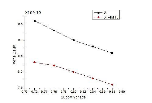
Fig -8: WriteDelayComparison
This study presents the design and analysis of a nonvolatilehybrid10T(6T-4MTJ)SRAMbitcellbasedonMTJ technology. The proposed cell is simulated using the HSPICE circuit simulator, followed by a comparative analysis with a conventional 6T SRAM bit cell. According to our findings, the MTJ-based SRAM bit cell achieves a significantreductioninpowerconsumptionby92%while enhancing overall stability by 19.49%. The 6T-4MTJ design demonstrates notable advantages, including faster read and write operations, improved stability, and low powerconsumption.
[1] Kanika, R. Sankara Prasad, Nitin Chaturvedi, S. Gurunarayanan “AlowpowerhighspeedMTJbasednonvolatile SRAM cell for energy harvesting based IoT applications”2018
[2] Sarthak Talwara, B. Mohapatrab, Mohammad Rashid Ansaric,“Performance Analysis of CMOS Technology”2020.
[3] Harshita Gehlot Mohd Ejaz Aslam Lodhi “Analysis of FinFET and CNTFET based Hybrid CMOS Full Adder Circuit” November2022.
[4] Mark T.Bhor Ian A.Young “CMOS Scaling Trends and Beyond”2017.
[5]PrashanthBarla, VinodKumarJoshi, SomashekaraBhat “Spintronic devices: apromising alternativetoCMOSdevices”2 December2021.
[ ] M.Abbasi EskandariS.GhotbP.Fournier “Impact of a ferromagnetic insulating barrier in magnetic tunnel junctions”8December2022.
[7] Yaojun Zhang Xiaobin Wang Hai LiYiran Chen “STTRAM Cell Optimization Considering MTJ and CMOS Variations”10October2011.
[8] Vinod Kumar Joshi,Prashant Barla,Somashekra BhatBrajeshKumarKaushik “FromMTJDevicetoHybrid CMOS/MTJCircuits:AReview”3September2020.
[9] Ramin RajaeiAlireza Gholipur “Low Power Reliable andNonvolatileMSRAMCellForFacilitatingPowerGating and Nonvolatile Dynamically Reconfiguration”2 March 2018.
[10] S.Hamsa N.ThangaduraiA.G.Ananth “Low Power Design Application by Magnetic Tunnel Junctions in Magnetoresistive Random Access Memory (RAM),21 June 2019
[11]JianxiaoYang,BeniotGeller,Meng Li TongZhang“An InformationTheoryPerspectivefortheBinarySTT-MRAM CellOperationChannel,6January2016.
[12] Bojan Jovanović Raphael M. Brum Lionel Torres “Mtj-Based Hybrid Storage Cells For “Normally-OFF and Instant-ON”Computing3September2015.
[13] Kanika MongaNitin Chaturvedi “A CMOS/MTJ based Non-volatile SRAM cell with Asynchronous Write Termination for Normally OFF applications”2 December 2021.
[14] S. Kushwaha D. Kumar M. Saw A. Islam “MTJ-Based Nonvolatile9TSRAMCell “ 14January2013.