
International Research Journal of Engineering and Technology (IRJET) e-ISSN: 2395-0056
Volume: 11 Issue: 06 | Jun 2024 www.irjet.net p-ISSN: 2395-0072
SIMULATION AND MODELLING OF NONISOLATED BIDIRECTIONAL ZERO-VOLTAGE-SWITCHING DC–DC CONVERTER
Mrs Anusree Shibindas, Mrs Usha Rebecca2
1 Assistant professor, Rajiv Gandhi Institute of Technology, Bengaluru, Karnataka, India.
2Assistant professor, Rajiv Gandhi Institute of Technology, Bengaluru, Karnataka, India
Abstract - A new nonisolated zero voltage switching(ZVS)bidirectionaldc-dcconverterisproposedinthis paper. Bidirectional converters have been widely used in variousindustrialapplicationssuchasuninterruptiblepower supplies, fuel cell vehicle, and satellite applications. A bidirectionalconvertercontrolsthepowerflowbetweenthedc busandthelowvoltagesourcessuchasback-upbatteries,fuel cell, and super capacitors. The proposed converter utilizes a very simple auxiliary circuit that consist of an additional winding to the main inductor and an auxiliary inductor to provide ZVS of the power switches and a ripple free inductor current. A comparative study between the conventional nonisolated bidirectional dc–dc converter and the proposed nonisolatedbidirectionalZVSdc–dcconverterisanalyzedand simulation is done in MATLAB software and the practical implementation of the proposed converter is done.
Key Words: Zero Voltage Switching (ZVS), Zero Current Switching (ZCS), Bidirectional DC-DC convertor (BDC), PWM generators, Coupled inductor.
1. INTRODUCTION
Bidirectional dc–dc converters have been widely used in various industrial applications such as renewable energy systems, hybrid electric vehicle, fuel cell vehicle, uninterruptible power supplies, and satellite. In such applications, bidirectional dc–dc converters control the powerflowbetweenthedcbusandthelow-voltagesources such as back-up batteries, fuel cells, and super capacitors. Bidirectional dc–dc converters are classified into isolated andnonisolatedversions.
In conventional nonisolated bidirectional dc–dc converter,itoperatesincontinuousconductionmode(CCM). The CCM provides a low ripple current. However, the switchinglossofthepowerswitchesislargeandthereexists thereverserecoveryphenomenonoftheantiparallelbody diode of thepower switch. With a smallerinductance,the conventional converter operates with an inductor current thatflowsinbothdirectionsduringeachswitchingperiod. Then ZVS operation of the power switches is achieved. However,largeinductorcurrentripplecauseslargevoltage ripple and shortens lifetime of low-voltage sources. However,toavoidreverserecoveryphenomenon,toachieve ripplefreeinductorcurrent,toreducevoltagerippleanew
nonisolated bidirectional converter is proposed in this paper.
1.1 Proposed Bi-directional DC-DC converter:
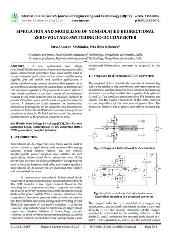
Theproposedbidirectionaldc–dcconverterisshowninFig1.Itisverysimilartotheconventionalconverterexceptthat anadditionalwindingNs tothemaininductorandauxiliary inductorLsareaddedandthefiltercapacitorCf issplitinto Cf1 andCf2.ThisauxiliarycircuitprovidesZVSfunctionand cancels out the ripple component of the main inductor current regardless of the direction of power flow. The equivalentcircuitoftheproposedconverterisshowninFig2.
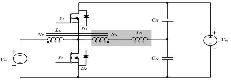
Fig -Error!Notextofspecifiedstyleindocument.: Equivalent circuit of the proposed converter
The coupled inductor Lc is modeled as a magnetizing inductanceLmandanidealtransformerthathasaturnratio of Np:Ns = 1:n. The leakage inductance of the coupled inductor Lc is included in the auxiliary inductor Ls. The diodesD1 andD2 representtheintrinsicbodydiodesofS1 and S2 . The capacitors C1 and C2 are the parasitic output
International Research Journal of Engineering and Technology (IRJET) e-ISSN: 2395-0056
Volume: 11 Issue: 06 | Jun 2024 www.irjet.net p-ISSN: 2395-0072
capacitancesofS1andS2.SincethecapacitancesofCf1andCf2 are large enough, Cf1 and Cf2 can be considered as voltage sources VCf1 and VCf2 during a switching period. Since the averageofthevoltageacrosstheinductorshouldbezeroat steady-state according to volt-second balance law, the averagevaluesoffiltercapacitorsvoltagesVCf1 andVCf2 are equaltovoltages(Vhi-Vlo)andVlo respectively.
2. DESIGN OF BDC
SpecificationVio =12V(Inputvoltage),Vhi =24V(Output voltage)

Table 1: Design values of BDC
Sl. No
1 Dutyratio(D) 0.5 0.5
2 Resistance(R) 5.76Ω 1.44Ω
3 Inductance(L) 45µH 45µH
4 Capacitance(C) 86.805µF 138.88µF
5
2.1 DESIGN OF COUPLED INDUCTOR
Specifications:
Input Voltage Vi = 24V, Output Voltage Vo = 12V at 8.33A, SwitchingFrequencyfs=10kHz,Magnetizingcurrentripple Δim =20%Im (demagnetizingcurrent=12A)DutycycleD= 0.5,TurnsratioNs/Np=0.3, AssumecopperlossPcu=1.5W,
Wire resistivity 6 1.724*m 10 c , Core cross
sectionalareaAc=1.09cm2 ,WindingfillfactorKu=0.3,Core MaximumfluxdensityBmax =0.25T,CorewindowareaAW = 0.256cm2
Components of magnetizing current referred to primary:= 0.3*(1/1-0.5)*(24/1.2) 12A,Δim =20%ofIm = 2.4A
Table -2: Design values of coupled inductor Sl. No Specifications Design value
Magnetizinginductance(Lm) 250µH
Windingcurrent(I) 17.07A 3 Primarynumberofturns(NP) 13Turns 4 Secondarynumberofturns(Ns) 4Turns
Wireguage 19AWG
Powerlossdensity(ΔB) 0.04W/cm3
Coreloss(Pfe) 0.25W
3 SIMULATION RESULTS
3.1 Conventional bidirectional DC-DC converter
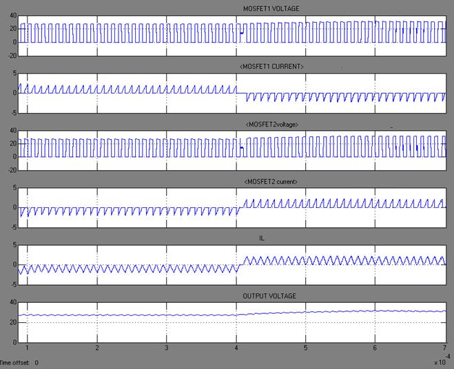
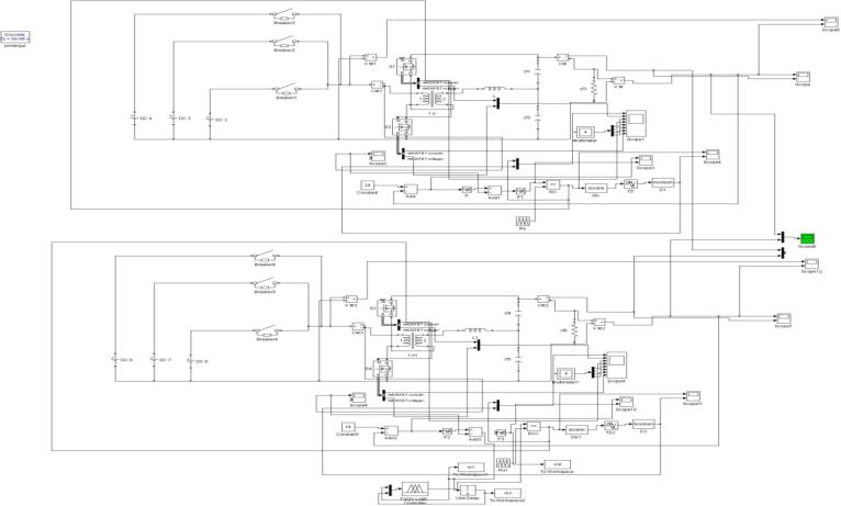
Fig-3 shows the simulink model of conventional bidirectionalDC-DCconverter,Fig-4showsthesubsystemto generate trigger pulses for switches S1 and S2, The simulation waveforms are in Fig-5, which gives the input voltageandoutputvoltagewaveforms.
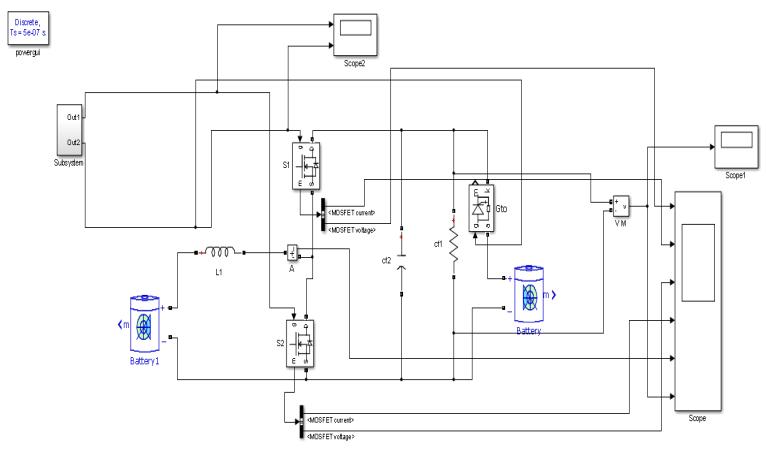
Fig –3: Conventional bidirectional DC-DC converter
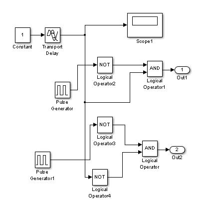
Fig –4: Subsystem: MOSFET switches S1 and S2 PWM generator
International Research Journal of Engineering and Technology (IRJET) e-ISSN: 2395-0056
Volume: 11 Issue: 06 | Jun 2024 www.irjet.net p-ISSN: 2395-0072
3.2 fuzzy PI controlled BDC
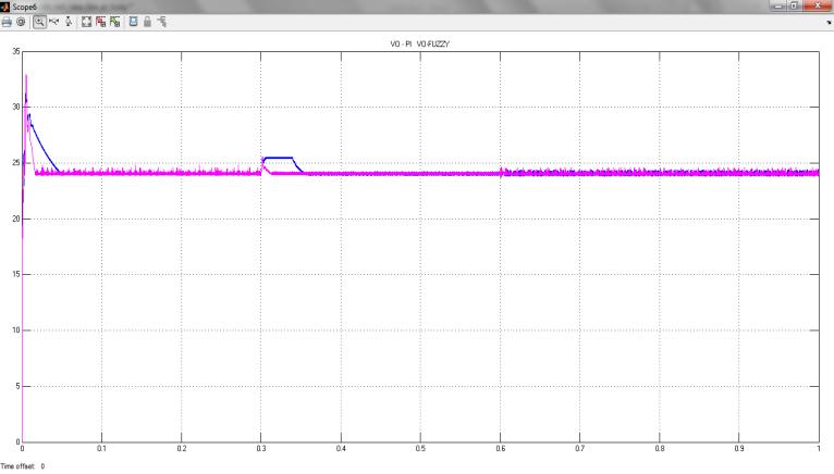
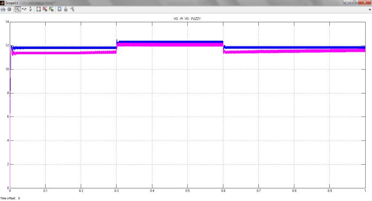
In Fig-6 proposed BDC boost mode line regulation is obtained by fuzzy, PI control. Fig-7 which gives the combinationofPIandfuzzyPIoutputwaveformofproposed boostmodeforlineregulation.Infuzzycontroltheoutput voltagesettlesfasterthanPIcontrol.
InFig-8proposedBDCbuckmodelineregulationisobtained byfuzzy,PIcontrol.Fig-7whichgivesthecombinationofPI andfuzzyPI outputwaveformofproposedbuck modefor line regulation. In fuzzy control the output voltage settles fasterthanPIcontrol.
4.
HARDWARE IMPLEMENTATION
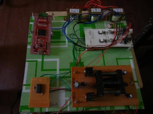
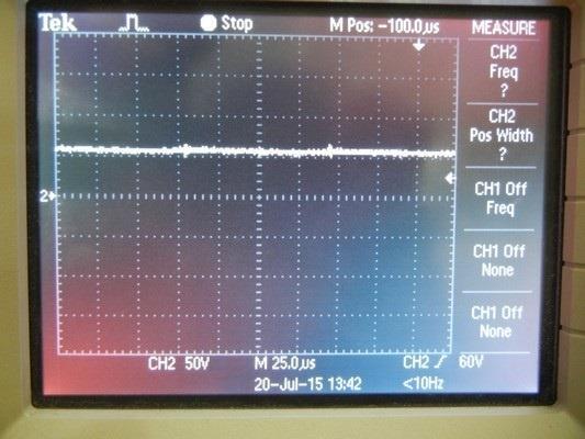
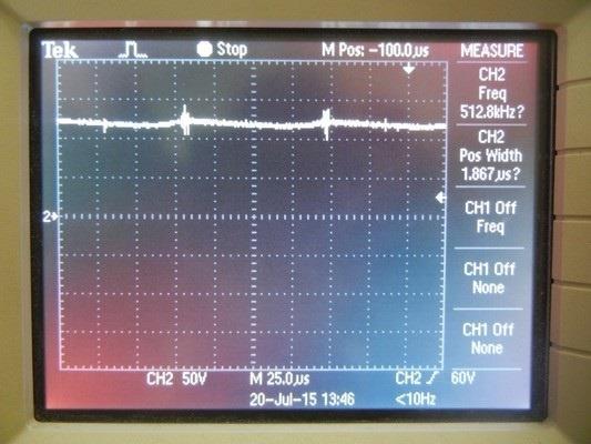
Figure-10showsthehardwareimplementationofproposed BDC using FPGA. Figure-11 shows an output voltage waveformof12Vinbuckmodeoperationwheninputof24V supply is given. Figure - 12 shows an output voltage waveform of 24V in boost mode operation when input of 12Vsupplyisgiven.
International Research Journal of Engineering and Technology (IRJET) e-ISSN: 2395-0056
Volume: 11 Issue: 06 | Jun 2024 www.irjet.net p-ISSN: 2395-0072
CONCLUSION
Simulation for conventional BDC and proposed BDC is simulatedinopenloopandclosedloopcontrolwithinput givenas12Vandoutputobtainedas24Vinboostmodeand input given as 24V and output obtained as 12V in buck mode.Insimulationforclosedloop(PIandfuzzyPI)control, line regulation is obtained by varying input voltages and outputvoltageisobtainedapproximatelyconstantas24Vin boostmodeand12Vinbuckmodeoperation.Comparedto fuzzzy and PI control the rise time and settling time is reduced in fuzzy.Hardware Implementation for proposed BDC is done using FPGA.In hardware implementation of boostmodeoperationaninputof12Vissuppliedandoutput of24Visobtainedandinbuckmodeoperationaninputof 24Vissuppliedandoutputof12Visobtained.
References:
[1]P.Das,S.A.Mousavi,andG.Moschopoulos,“Anaysisand design of a nonisolated bidirectional ZVS-PWM DC–DC converter with coupled inductor,” IEEE Trans. Power Electron.,vol.25,no.10,pp.2630–2641,Oct.2010.
[2]H.Kim,C.Yoon,andS.Choi,“Animprovedcurrent-fed ZVSisolatedboostconverterforfuelcellapplications,”IEEE Trans.PowerElectron.,vol.25,no.9,pp.2357–2364,Sep. 2010.
[3] H. Tao, J. L. Duarte, and M. A. M. Handrix, “LineinteractiveUPSusingafuelcellastheprimarysource,”IEEE Trans. Ind. Electron., vol. 55, no. 8, pp. 3012–3021, Aug. 2008.
BIOGRAPHIES


MrsAnusreeShibindas
AssistantProfessor RajivGandhiInstituteofTechnology Bengaluru–560032.
MrsUshaRebecca
AssistantProfessor RajivGandhiInstituteofTechnology Bengaluru–560032.