

Design and Performance Analysis of CMOS Voltage Controlled Oscillator (VCO) in Static CMOS 45 nm Technology
Ajay J, Hemanth Joshi, Rajath Nayaka B M and B P Harish
Department of Electronics and Communication Engineering, University Visvesvaraya College of Engineering, Bangalore University, Bangalore, India ***
Abstract:
This paper presents a relative study among different topologies of Ring Oscillator based Voltage Controlled Oscillator (VCO) on the basis of different parameters like centre frequency, tuning range, frequency stability, power dissipation and linearity etc. All the design has been done in 45 nm Static CMOS technology and are subsequently compared on various parameters. An inherent idea of the given performance parameters has been realized by the comparative study. The comparative data shows that VCO with both NMOS & PMOS control devices along with complementary Vctr has the best trade-off between power dissipation and tuning range. In this study the topology of VCO with complementary control voltages exhibits tuning range of 0-20 GHz and power dissipation less than 1.5mW thus eliciting Ring oscillator based VCO is best in terms of power consumption. Simulations are carried out using the LTSpicesimulatorina45nmstandard process.
Keywords: Voltage Controlled Oscillator (VCO), Static CMOS, Tuningrange,Powerconsumption.
1 Introduction
In today’s IC industry a good understanding of semiconductor process and devices is essential, as process to device to circuit domains are tightly coupled, for quality of analog / digital designs. In digital designs MOStransistorsareconsideredassimpleswitchesbutin analog designs detailed understanding of the device is required because of its multiple roles as amplifying device, capacitor, switch etc. and this implication of the second order effects on the performance of circuit. Further, with the advent of device scaling into nanometer regime, implications of non-ideal effects become significant and the circuit designer has to decide on the selection of second order effects to be considered for design. At nanoscale integration, the CMOS technology has become a technology of choice for analog circuit designinamixedsignalenvironment.
SinceallthebasicdevicesinanICrespondtocontinuous time stimulus, analog design forms the foundation for all IC designs. Modern IC technology presents many design challenges. There is significant variability in the manufacturing process for advanced technology nodes. The actual operation of the large number of devices on advanced ICs also causes variability. This variability manifests as changes in the device threshold voltage, supply voltage, operating temperature, which in turn
translate into performance variability. Densely packed devices result in parasitic capacitances leading to undesirablesignalinterferenceanddistortion.
InthedomainofVLSIdesigntheselectionofalinearand wide range voltage-controlled oscillator for various RF, Biomedical,Clockrecoverycircuitsandotherapplications isalwaysachallengingworkforElectronicsEngineers.An oscillator is an electrical autonomous system which generates a periodic oscillating frequency signal depending on its input voltage. VCO is the main component in many RF circuits and is the heart of Phase Lock Loop system, Clock recovery circuit and Frequency Integratedcircuits,soitisveryvitalto selectthesuitable VCOdesign. Frequency,amplitudeandnoiselevel should becontrolledformanyoftheapplications.
Oscillatorscanbedividedintotwocategories;Firstly,the LC oscillator which is composed of the active devices, coupled with LC resonant circuit. Secondly, the loop ring oscillator which is composed of delayed cascade units with positive feedback. The important requirements of VCO are High gain, wide tuning range, low power consumptionandhighsignaltonoiseratio.
The design of a Voltage Controlled Oscillator involves many trade-offs between area, speed, power, and application domains. These problems and a comparative study of different ring oscillator designs is midst interest in this paper. The performance of different circuits has been comparatively analysed through simulation results in45nmCMOSTechnologyusingLTSpice
2 Simulation Methodology
2.1
Ring Oscillator Design:
The design of the ring oscillator can be done using three inverters. The three-stage ring oscillator with 3 inverter stages connected in series to form a positive feedback system to provide sufficient gain to support sustained oscillations. The frequency of oscillations is given in Eq. (1.1).
f=1 τ………………...…(1.1)
whereτ=timedelayforsingleinverter, n=numberofinvertersintheoscillator.
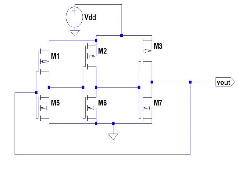
Fig 2.1: Schematic Circuit Diagram of 3 Stage Ring Oscillator.
According to Barkhausen criteria, the necessary but not sufficient condition for positive feedback circuit to oscillateis:
1.Themagnitudeofloopgain,|H(j��0)|≥1
2.Thephaseshiftaroundtheloop,∠H(j��0)=2nπ where ��0 is the frequency at which the circuit may oscillateinrad/s.
Table 2.1 Mentions the effects of device sizing on performance metrics of 3-stage ring oscillator.
2.2 VCO with NMOS control Devices
IntheVCOtopologywithNMOScontroldevices,shownin Fig., an NMOS control device (M7, M8, and M9) are stacked below the NMOS (M4, M5, M6) of basic inverter stageoftheROandtheinputcontrolvoltageisappliedto these control devices. The NMOS control devices transitionbetweencutoff,saturationandtrioderegionas DCcontrolvoltageislinearlyvariedfrom0VtoVDD
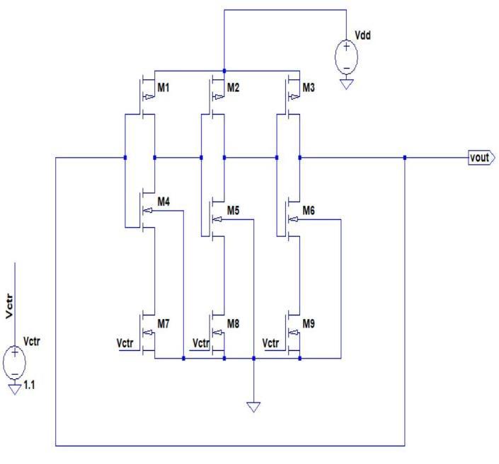
Fig 2.2: Three-stage VCO with NMOS control devices.
1.For < ,control devices are biased in thecut off region. Thus, there is no drain current and hence no oscillations.
2.For ,M7,M8andM9turnoninthesaturation region. Drain current in saturation region for NMOS deviceshasasquare-lawdependenceon ,asgivenin Eq.(2.1).
3.As isincreasedfurther,i.e.,as of control devices, NMOS control devices enter the triode region. Here, the drain current isa linear function of andisgivenbyEq.(2.2).
(2.2)
( =0.466V)
Graph 2.2: Transfer characteristics of the NMOS controlled VCO circuit
The VCO exhibits a dead zone, with no oscillations, up to asM7,M8,andM9arebiasedincutoff.As increases beyond the frequency increases with a International Research Journal of Engineering and Technology (IRJET) e-ISSN:2395-0056 Volume: 11 Issue: 06 | Jun 2024 www.irjet.net
International Research Journal of Engineering and Technology (IRJET) e-ISSN:2395-0056
Volume: 11 Issue: 06 | Jun 2024 www.irjet.net
steepslopeduetothesquare-lawdependence ofcurrent on
Table 2.2 Mentions the effects of device sizing on performance metrics of VCO with NMOS control devices (at
2.3 VCO with PMOS control devices
In this topology, PMOS control devices (M1, M2, M3) are stacked above the PMOS devices (M4, M5, M6) of the basicinverterstageRO.Theinputcontrolvoltageisused as gate control for PMOS control devices. The devices switch from cutoff to saturation and eventually to triode regionascontrolinputisdecreasedfrom to0V.
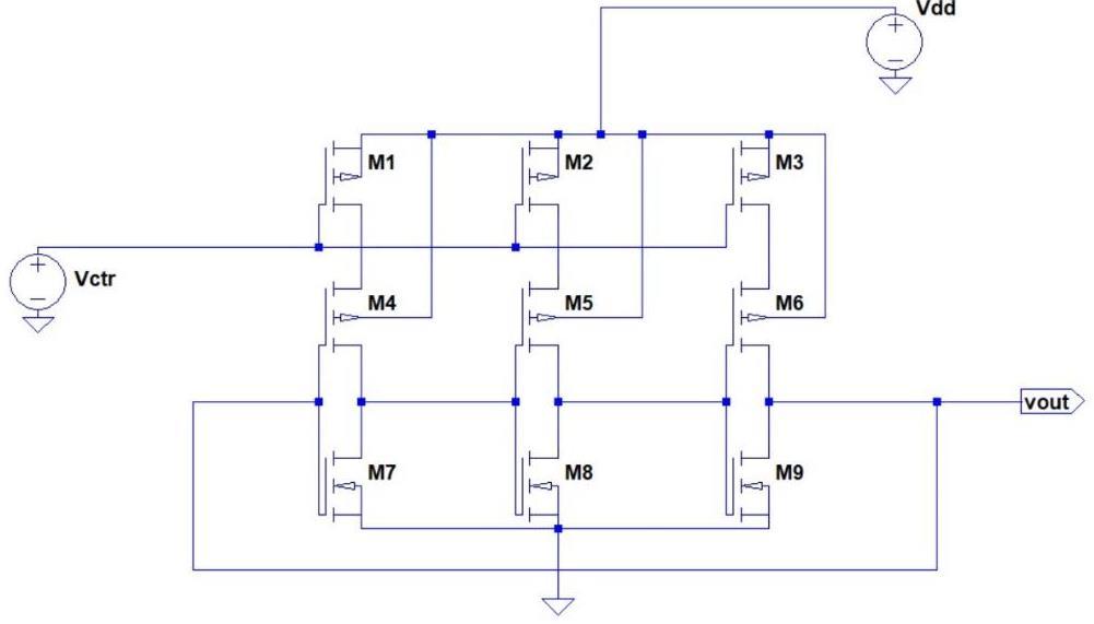
Fig 2.3: Three-stage VCO with PMOS control devices. theoperationofthecontroldevicesindifferentoperating regionsarementionedbelow:
1. For 0 < < | |, the PMOS control devicesareinthetrioderegion.Herethedraincurrent isalinearfunctionof
|)…….…...(2.3)
2. For | | | |, M1, M2 and M3 are biased in the saturation region. Drain current in saturation region for PMOS devices has a square-lawdependenceon
(2.4)
3. The control devices enter cut off region for > . Thus, the drain current is zero and hencenooscillationsareexpected.
Graph 2.3: Transfer characteristics of the PMOS controlled VCO circuit.
Similar to the previous circuit, the characteristics have a low slope when the device is in the triode region and a greater slope when in the saturation region. The VCO exhibits a dead zone for > Thus, there is significant nonlinearity throughoutthetuningrange. The circuit has to be sized carefully to avoid asymmetry in riseandfalltimes.
Table 2.3 Mentions the effects of device sizing on performance metrics of VCO with PMOS control devices (at
International Research Journal of Engineering and Technology (IRJET) e-ISSN:2395-0056 Volume: 11 Issue: 06 | Jun 2024 www.irjet.net
2.4 VCO with both NMOS and PMOS control devices using same
In this circuit, both NMOS (M10, M11, M12) and PMOS (M1, M7, M3) control devices are stacked in series with eachringoscillatorstageasshowninthecircuitdiagram. All NMOS / PMOS control devices are given the same controlvoltage.
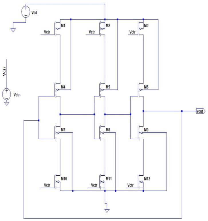
Fig 2.4: VCO with same control voltage to both PMOS and NMOS devices.
1. For 0 < < the NMOS devices turned off whereasthePMOScontroldevicesareinlinearregion. Hence there is no drain current through the devices andnooscillationsareobtained.
2.For < < - - | ,NMOSdevicesturn on in saturation while PMOS devices remain in triode region.Thedraincurrentstartincreasingwith .
3.For - - | < < + , both devices are in saturation region. The drain currents are highestinthisregion.
4. For + < < - , PMOS devices remain in the saturation region while NMOS devices enter the triode region. The drain current begins to decreasewithincreasing
5. For - < < the PMOS control devices are turned off whereas the NMOS devices are in the linearregion.Hencethereisnodraincurrentthrough thedevicesandnooscillationsareexhibited.
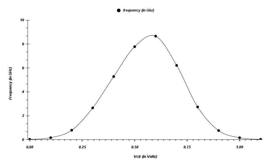
Graph 2.4: The variation of frequency as a function of control voltage. It is a bell-shaped characteristic.
Table 2.4 Mentions the effects of device sizing on performance metrics of VCO with NMOS & PMOS control devices (at =0.6V).
2.5 VCO with both NMOS & PMOS control devices & complimentary
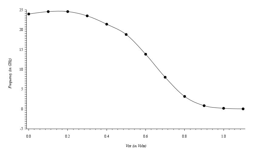
The drawbacks of the previous circuits can be overcome by simply using two complimentary control voltages instead of one. The control inputs are such that while NMOS control devices (M10, M11, M12) are applied by ,PMOScontroldevices(M1,M2,M3)aregivenagate voltagecomplementarytothatgiventoNMOS( = - ).
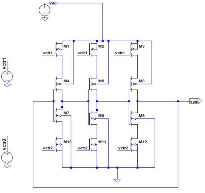
Fig 2.5: VCO with Complementary control Voltage to both PMOS and NMOS devices
1. PMOS control devices are cut off for < | |. Henceoscillationswillnotoccur.
2. When increases further, for > | |, both NMOSandPMOScontroldevicesturnoninthesaturation region.
3.Thedeviceseventuallyentertrioderegionwhen > + .
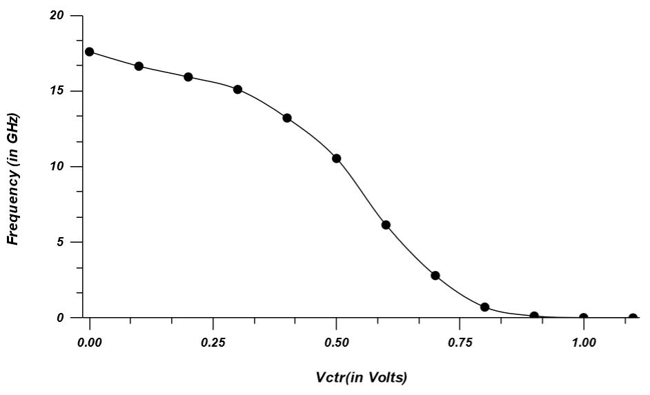
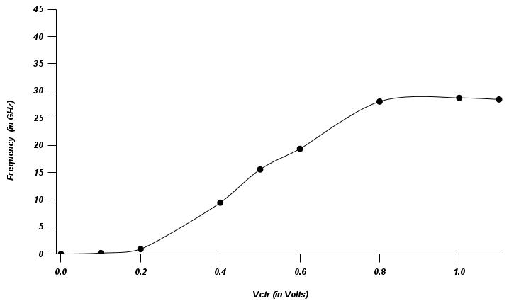
Graph 2.5: Variation of Frequency with voltage for complementary control Voltage given to both PMOS & NMOS.
The circuit can oscillate ata frequency much higher than that using a single control voltage. It is a monotonically increasing curve with a wider tuning range. The input voltage range allowable for this circuit can be twice as muchasthatforthepreviouscircuit.
Table 2.5 Mentions the effects of device sizing on performance metrics of VCO with complementary in NMOS & PMOS control devices (At = 0.2V & = 0.9V).
Results and Discussions
An Overview of circuits
The frequency of oscillations increases for decreasing device widths. This is because the effect of decreasing load capacitance is more dominant compared to that of decreasing drain currents. From Table 2.1, it can also be observed that, with decreasing device sizes, dynamic power dissipation of the circuit decreases because of the smaller currents through the circuit domination over increasing frequency. Thus, this is the rare case in CMOS designwherespeeddoesnottradewithpowerequations given below show the dependence of speed and power dissipationonloadcapacitances.
VCO with NMOS control devices.
This topology has a high center frequency of 13.88 GHz and a tuning range of 0 – 30 GHz. It can be further optimizedtoobtainhighercenterfrequenciesandtuning ranges. The tuning characteristic is non-linear due to the switching of the control device between operating regions. The dynamic power dissipated in the circuit at the center frequency ( ) is 3.938 mW. Note that the dynamic power dissipation is less than 12.25 mW for all frequenciesinthecharacteristicsgiveninTable2.2
VCO with PMOS control devices.
WhenPMOScontroldevicesareused,atuningrangeof0 – 25GHz with a center frequency of 12.517 GHz is obtained.Thereductionin andtuningrangeisbecause PMOS devices are inherently weaker than NMOS devices due to smaller hole mobility. The center frequency and tuning range can be further optimized by sizing the device's non-linearity. The dynamic power dissipated in the circuit at is 1.29 mW. The dynamic power dissipationislessthan9.56mWforallfrequenciesinthe characteristicsgiveninTable2.3. International Research Journal of Engineering and Technology (IRJET) e-ISSN:2395-0056 Volume: 11 Issue: 06 | Jun 2024 www.irjet.net
International Research Journal of Engineering and Technology (IRJET) e-ISSN:2395-0056
Volume: 11 Issue: 06 | Jun 2024 www.irjet.net p-ISSN:2395-0072
VCO with both NMOS and PMOS control devices using same .
WhenbothNMOSandPMOScontroldevicesareusedand the same control voltage is applied to the gate of all control devices, the tuning range of 0 – 10 GHz with a centre frequency at 5.02 GHz is achieved. The circuit shows bell-shaped characteristics with two dead zones, thusrestrictingtheallowablecontrolvoltagerangetoless than /2. Non-linearity in the characteristics can be reduced by ensuring that NMOS/PMOS control devices are in the saturation region for the entire range of the controlvoltageapplied.Thedynamicpowerdissipationis less than 6.76 mW owing to the lower frequencies at whichthecircuitoperates.
VCO with both NMOS & PMOS control devices with complementary
Applying complementary voltages to NMOS and PMOS control devices resulted in a tuning range of 0 – 18 GHz withacentrefrequencyof9.51GHz.Thetuningrangecan be further widened by sizing the devices appropriately. Again, the characteristics are non-linear owing to the switchingofdevicesbetweenoperatingregions.At ,the dynamic power dissipation is 1.556 mW, while it is less than10mWforallfrequencies.
Table 3 Comparative study of performance metrics of VCO with multiple control schemes.
TheperformanceanalysisoftheVCOcharacterizedbyits centerfrequency,tuningrange,frequencystability,power dissipationandlinearityhasbeencarriedout.
In CMOS analog design, selection of the CMOS process, selection of circuit topology and sizing of the devices provide decent design choices to optimize the performance and to meet the user specifications. In the chosentechnology,thecomplimentary inbothNMOS PMOS circuits it is found that while sizing the devices thereisatrade-offbetweenpowerdissipationandcenter frequency. Similarly, there are trade-offs between frequency stability, linearity and tuning range. In this topology,variationwithfrequencystabilityisfoundtobe good.
References
1. Behzad Razavi, “Design of analog CMOS integrated circuits”, Tata McGraw-Hill Publishing, Revised Edition, 2016.
2. G. Jovanovic, Stojcev, Stamenkovic, "A CMOS Voltage Controlled Ring Oscillator with Improved Frequency Stability",ScientificPublicationsoftheStateUniversityof NoviPazar,Vol.2,I(2010).
3.VandanaSikarwar,NehaYadav,ShyamAkashe,“Design and analysis of CMOS ring oscillator using 45 nm technology”, 3rd IEEE International Advanced Computing Conference(IACC),2013,pp.3-5.
4. Rupesh Kumar Patlani, Rekha Yadav,” Design of low power ring VCO and LC – VCO using 45 nm technology”, International Journal of Innovative Science, Engineering andTechnology(IJISET),2014,pp1-2.
5. B.S. Patro, J.K. Panigrahi, Sushanta K. Mandal,” A 6–17 GHz linear wide tuning range and low power ring oscillator in 45nm CMOS process for electronic warfare”, InternationalConferenceonCommunication,Information &ComputingTechnology(ICCICT),2012,pp.5-7.
6. Sajotra Deepak, Dhariwal Sandeep, Mishra Ravi Shankar” Comparative Analysis of Voltage Controlled Oscillator using CMOS”, Indian Journal of Science and Technology,Vol9(14),pp.5-8.
7.JanM.Rabaey,A.ChandrakasanandB.Nikolic, “Digital Integrated Circuits: A Design Perspective”, Pearson Education,2003.
Conclusion
Inthiswork,a3-stageCMOSvoltage-controlledoscillator hasbeendesignedandimplementedin45nmtechnology. Two designs have been proposed for the same topology design optimized for tuning range and design optimized forcenterfrequency.
8. H. A. Mahmoud and M. A. Bayoumi, “A 10-Transistor Low-PowerHigh-SpeedFullAdderCell”,in Proceedings of IEEE International Symposium on Circuits and Systems,pp. 43-46,1999.