
International Research Journal of Engineering and Technology (IRJET) e-ISSN:2395-0056
Volume: 11 Issue: 05 | May 2024 www.irjet.net p-ISSN:2395-0072


International Research Journal of Engineering and Technology (IRJET) e-ISSN:2395-0056
Volume: 11 Issue: 05 | May 2024 www.irjet.net p-ISSN:2395-0072
Uday Singh1, Kamalesh Singh2, Dr. Vikas Nehra3, Dr. Kusum Dalal4
1B.Tech Student, Department of Electronics and Communication Engineering, Deenbandhu Chhotu Ram University of Science and Technology (DCRUST), Murthal, Sonipat, Haryana, India
2Scientist/ Engineer ‘SD’, Semi-Conductor Laboratory, S.A.S Nagar, Punjab, India
3Assistant Professor, Department of Electronics and Communication Engineering, DCRUST, Murthal, Sonipat, Haryana, India
4Assistant Professor, Department of Electronics and Communication Engineering, DCRUST, Murthal, Sonipat, Haryana, India ***
Abstract: This paper presents a review of the capacitive pressure sensor. Firstly, the different types of sensors available are compared. For applications requiring high sensitivity and very low effects due to temperature, the capacitive sensor is preferred. Various methods to change the capacitance are also compared, which leads to the conclusion that the method involving changing the distance between the plates has the highest sensitivity. The different diaphragms available are also compared in this paper. The result of the comparison shows that the square diaphragm is most suitable. Further study shows that the diaphragm with a bossed structure has the highest sensitivity and the lowest nonlinearity. After the structural analysis, the pull-in effect phenomenon present during anodic bonding is also studied. The analysis of the pull-in effect showed that the dimension of the sensor should be chosen such that the electrodes do not stick during the anodic bonding. Different capacitive sensing schemes are also shown in this paper. The parasitic capacitances and the noise are major factors limiting the performance of the sensor. So the sources and methods to mitigate such effects are also presented. The ASICs available for the conversion of the capacitance to voltage or digital output are compared based on different parameters.
Key words: Capacitive pressure sensor, sensitivity, nonlinearity, bossed diaphragm, pull-in effect, differential structure, capacitance to voltage circuit
MEMS stands for microelectromechanical systems. MEMS technology combines microelectronics and mechanical systems. MEMS sensors and actuators are used in almost every modern system. MEMS sensors haveaccommodatedamajorpartofthesensormarketin recent years and are fast developing with new capabilities. The MEMS pressure sensors are being used in various areas like biomedical, defence, automobile, consumer products, industries, and many more civilian anddomesticapplications.MEMSpressuresensorsclaim 72% of revenue, medical electronics at 12%, industry segments at 10%, and the rest 6%, split between consumer electronics and military/aerospace
applications. The current pressure sensors are being used in the pressure range from a few Pascals to mega Pascals. The sensors are to being used in the temperature ranges between – 25 oC to 125 oC and advancements are being made to operate the sensors above 600 oC. Among the various pressure sensors, piezoresistive and capacitive sensors are widely used. Piezoresistive pressure sensors provide high sensitivity, and they have linear operation for a wide range of pressure. Capacitive pressure sensors are preferred as they provide high sensitivity and the change due to temperature is very small. MEMS pressure sensors include a flexible diaphragm that deforms on the application of pressure, and this deformation is converted to an electrical signal, generally voltage or digital signals.Bulk micromachiningisgenerallyusedto create the silicon membrane in the pressure sensors. Piezoresistors are patterned across the diaphragm. The sensor is generally designed and packaged so that the topsideof the diaphragmis exposed tothe environment for the application of pressure. (Balavalad et al., 2015) The change in pressure forces a deformation of the diaphragm; this deformation results in a change in resistance of the piezoresistors and, in turn, a change in voltage by on-chip electronics (Wheatstone bridge). Capacitive sensors consist of a fixed electrode and a movable electrode, The movable electrode displaces undertheappliedpressure, whichresultsina changein capacitance. The change in capacitance depicts the appliedpressure.
Thispaperaimstoprovideareviewofthetechnological advancements in pressure sensor technology. The main focusofthis paperisthecapacitive pressuresensor, the advancements in its structure, and various factors affectingitsdesign.
2. Evolution of the mems pressure sensor
The first developed pressure sensors was a metal strain gauge. This sensor is still being widely used in the mechanical transducers used in the industries. These

International Research Journal of Engineering and Technology (IRJET) e-ISSN:2395-0056
Volume: 11 Issue: 05 | May 2024 www.irjet.net p-ISSN:2395-0072
sensors change their resistance on the application of force,pressureoranyexternalphysicalquantityleading to the deformation in the sensor (Hilal M & Mohamed.S. 2011).
Strain gauges were made of metal foil as well as metal wireinthesesensors. (Baoetal.,2005)thestraingauge sensors were fabricated by conventional machining technique The effect of the metal strain gauge is isotropic.(OluwoleO.Oetal.,2015)carriedoutauniaxial stress analysis testing with the designed strain gauge measurement instrument on a clamped wooden beam thathasamodulusofelasticity10700 N/mm2,lengthof 250mm and cross-sectional area of h = 4.5 mm , b = 25mm applying load in an incremental succession, the strain and stress at different load interval was determined.Forappliedload0.9806Nthe experimental strainvaluewas250.14×10-6 whilethetheoreticalstrain value was 271.54 ×10⁻⁶ and for applied load 1.4709 the experimental strain value was 362.12×10⁻⁶, while theoretical strain value was 407.31×10⁻⁶ (Isrel et al., 2021)performedexperimentalstressanalysiswithafull wheatstone bridge created with strain gages. The analysis involved stepwise stress measurement by keeping the application piece with Wheatstone bridge connection by increasing from 5-50 kN with 5 kN increments for certain periods of time. The results showedastrainof22.95MPafor50kN.
In1954thepiezoresistanceeffectinthesemiconductors was discovered by S.C Smith. He discovered that the change in the resistance in semiconductors like silicon and germanium was higher than in the metal strain gauges. This higher change was due to the fact that the change in the resistance in the piezoresistors based on semiconductor was basically due to the change in the resistivity of the material rather than change in resistance due to geometric deformation as in the metal strain gauge sensors. Therefore the effect of the piezoresistances was two order higher than the metal strain gauge sensors (Bao et al., 2005). The resistivity change in piezoresistors is due to changes in interatomic spacing resulting from strain which affect thebandgaps, making it easier (or harder depending on the material and strain) for electrons to be raised into theconduction band as reported in [3] The effect of piezoresistanceisgenerallyanisotropic.Withinacertain range of strain this relationship is linear, so that the piezoresistivecoefficientareconstant[3]
With the discovery of piezoresistance effect, it was realized that the large effect of resistance change in this effect would have important applications in sensors, especially in the mechanical sensors which were dominatedatthattimebymetalstraingaugesensor.
(Jingetal.,2020)preparedapiezoresistivesensorbased onthegraphene-PDMS@spongebyfixinggrapheneona sponge skeleton using PDMS. This piezoresistive sensor exhibited high elasticity (strain up to 85%), high sensitivity (0.075 K Pa 1), a wide responding range (0–50KPa)andhighstability(2000cyclespressuretest).
(Zhang et al., 2016) reported a simple process to manufacture a piezoresistive sensor with high elasticity. The process was based on repeatable dipping and coating. The sensor was based on a homogeneous 3D hybrid network of carbon nanotubes@silver nanoparticles (CNTs@Ag NPs) which were anchored on a skeleton sponge. The sensitivity of the sensor was increasedtoagreatextentafteraddingmoreAgNPs.For the ratio of 1:20, the sensitivity was 2.12 kPa 1 at 2.24−11kPaandabout9.08kPa 1 at11−61.81kPa.
(Tianetal.,)reportedthataflexiblepiezoresistivetactile sensor can exhibit a sensitivity up to 0.96 kPa-1 by integrating two face to face laser patterned graphene films.(Pangetal.,)reportedamechanicalsensorachieve pressure and strain-sensing properties with a combination of graphene porous network (GPN) and polydimethylsiloxane (PDMS),whichshowsa sensitivity of0.09kPa-1
(Lee et al., 1982) presented a batch-fabricated silicon capacitive pressure transducer with low temperature sensitivity. It also reported temperature coefficients of thezero-pressureoffsetvoltagehave beenequivalentto between 1 and 5 mmHg/oC, while typical temperature coefficients of the pressure sensitivity have been from1500 to - 4000 ppm/oC, depending on the resistor dopinglevel.
Therefore capacitive pressure sensor is better due to reduced temperature sensitivity and increased sensitivity.
Piezoelectric sensor is based on the principle of conversion of the deformation in the material to the voltage unlike piezoresistive which converts the deformation to resistance. Materials like single crystalline material (such as quartz), (piezoelectric semiconductor (such as ZnO2), tourmaline, and Rochelle salt have this property to produce voltage on the

International Research Journal of Engineering and Technology (IRJET) e-ISSN:2395-0056
Volume: 11 Issue: 05 | May 2024 www.irjet.net p-ISSN:2395-0072
application of pressure or force leading to strain in the material. This piezoelectric effect was discovered by PierreCuriein1880butthe manufacturersbegintouse the piezoelectric effect in 1950. The piezoelectric effect was not used till early 20th century due to the developmentofelectronic oscillatorandamplifierinthe early 20th century which were used to drive the piezoelectric element. Since then, this measuring principle has been increasingly used, and has become a mature technology with excellent inherent reliability as reported in [8]. There is formation of electric charge across the faces of the piezoelectric material on the application of the pressure, this electric charge can be measuredasthevoltageacrossthefacesofthematerial. (Kim et al., 2022) a stretchable piezoelectric strain sensor was developed by introducing a kirigami pattern toachievestretchabilityinarigidPVDFfilm.Inaddition to the sensor developed a circuit was also designed to measure the output voltage generated due to the strain formation accurately and consistently.The kirigami piezoelectric sensor fabricated had a sensitivity of 9.86 V/cm2 and stretchability of 320.8%, the highest values reported to data for kirigami piezoelectric strain sensors. (Zhang et al., 2016) developed a sensor consisting of different capacitors whose capacitances becamemuchlargerthanthatofthepiezoelectricquartz sensor which was in parallel with the quartz sensor. With this method, the data of the sensitivity enhancement of piezoelectric sensors were obtained. Experimental results in this study showed that the sensor sensitivity was increasedfrom4.00pC/N to4.07 pC/N when the capacitance of parallel capacitors was increasedfrom500to1000andthen5000timesof that ofthesensor.Theforcesensorsensitivitywasimproved by1.75%. Thissensoralsohasthelowestresponsetime.
There is also an inverse piezoelectric effect where applyingavoltagetothematerialleadstodeformationof thesensorstructure.
The next major development in the sensors was the development of the capacitive pressure sensor. The capacitive pressure sensor is based on the principle of capacitancechangingontheapplicationofpressure.
TheCapacitanceofthecapacitorisgivenby:
(Shivaleela.G et al., 2017) proposed a MEMS based capacitivepressuresensor using1-spring,4-springsand 9-springshasbeendesignedhavinga squarediaphragm oflength10,000µm×10,000µmandthicknessof525µm using Finite Element Method (FEM). The simulation results showed that the 9- springs capacitive pressure sensor model achieves a good and high sensitivity of 1.010e0pF/pa with displacement of 3.288e-5 µm at appliedpressureof1Paascomparedto1-springand4springcapacitivepressuresensors.
(Lee etal.,1982) Thecapacitancechangeina capacitive sensor for temperature input is negligible. The resulting temperature coefficient of sensitivity (TCS) is -6950 ppm/oC and the temperature coefficient of offset (TCO) is - 1600 ppm/oC, which is equivalent to about -2 mmHg/oCnearroomtemperature.
(Shaikh et al., 2008) presented a comparative study betweenthecapacitiveandpiezoresistiveMEMSsensors for pressure measurement. He observed that the sensitivity curve of piezoresistive is steeper than that of capacitive pressure sensor piezoresistive pressure sensor sensitivity changes up to 180 mmHg whereas capacitive pressure sensor sensitivity changes up to 335mmHg.
Therefore capacitive pressure sensor is preferred over piezoresistive sensor because it has various advantages over piezoresistive and other sensors such as less temperature dependent and have low energy consumptionwhereasthepiezoresistivepressuresensor is temperature dependent and have large energy consumption. Another advantage of the capacitive pressure sensor is to be able to detect larger pressure changes than the piezoresistive sensor. The capacitive pressure sensor also has higher accuracy and faster responsetimesduetosmallcapacitancesinvolved.
The major disadvantages of capacitive sensor are susceptible to EMI, parasitic capacitances and low sensitivitythanpiezoresistivesensors.
Table – 1: Comparisonbetweenthesensors[8]–[11]
Properties
Strain Gauge Piezores istive
Type
Piezoelec tric Capaciti ve
Principle Change in Reistan ce Change in Resistivit y Formatio nof electric charge Change in Capacita nce
Pressure
(21kPa to150
kPa to70
(250Pa to70

International Research Journal of Engineering and Technology (IRJET) e-ISSN:2395-0056
Volume: 11 Issue: 05 | May 2024 www.irjet.net p-ISSN:2395-0072
Sensitivity
Linearity
te
e
Therefore for pressure sensing applications capacitive senor is preferred as it has widest pressure range, high sensitivityandinsensitivetotemperature.
3. Capacitive pressure sensor
3.1 Methods to change the capacitance
3.1.1Changingthedielectricmedium
The capacitanceis directly proportional to thedielectric medium of the capacitor. Therefore by changing the dielectric constant between the electrodes the capacitance can be changed. For the application of the pressure sensor the dielectric between the electrodes needstobedisplacedontheapplicationofthepressure.
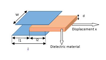
Fig.1:Displacingthedielectric
When displacing the dielectric, change in capacitance is . The dielectric constant of the material being displaced is . So the change in capacitanceisdirectlyproportionaltothedisplacement.
The dielectric is an insulator that gets polarized under the application of electric field. Due to this polarization there is an electric field generated field inside the dielectric medium in the direction opposite to the external electric field. This results in increase in the capacitanceofthesensor
This method is used generally by using different geometries of the dielectric between the electrodes and changingthedistancebetweentheelectrodes.
(Chaurasia et al., 2017) proposed a novel parallel plate capacitor having a droplet of dielectric in between the electrodes. On the application of the pressure the distance between the electrodes is decreased and the contact area between the electrode and the dielectric is increased. This resulted in enhanced sensitivity of 28
(Chhetry et al., 2017) has designed a flexible and highly sensitive capacitive pressure sensor which was also fabricated by coating a microporous polydimethylsiloxane(PDMS)elastomericdielectriconto conductive fibers. The designed capacitive pressure sensor had two microporous PDMS-coated fibers which were cross-stacked to function as a capacitive sensor. This sensor responds to compressive stress. As on applying stress due to any external agent the contact areawasincreasedandtheseparationbetweenthefiber electrodes was decreased. The developed sensor produced relatively high sensitivity of 0.278 kPa_1 for a lowpressureregion(<2kPa)
(Kim et al., 2022) developed a highly sensitive and flexible capacitive pressure sensor based on the porous Ecoflex,whichhasanalignedairgapstructureandcanbe manufactured by simply using a mold and a microneedle. Three different ranges: low-pressure range (1–500Pa),middle-pressurerange(500–15kPa),andhighpressure range (15–100 kPa) were selected as per the requirements Thefabricatedsensorbasedontheporous Ecoflex and an aligned airgap structure showed a linear response in all three pressure range. The sensitivities of the developed sensor were 1.277 kPa-1, 0.045 kPa-1, and 0.022kPa-1
In this method the pressure is applied normal to the electrode surface and the distance is changing. The change in capacitance is linear but the sensitivity is lower than the method to change the distance between theelectrodes.
3.1.2Changingtheoverlaparea
The capacitance of the sensor is directly proportional to theoverlapareaofthecapacitor.Thereforechangingthe overlap area results in change in the capacitance of the sensor. This method is preferred to transduce large displacements as larger travel range is available for the capacitiveplates.(Boseretal.)Thechangeincapacitance w.r.t pressure is linear in this method but has low sensitivity

International Research Journal of Engineering and Technology (IRJET) e-ISSN:2395-0056
Volume: 11 Issue: 05 | May 2024 www.irjet.net

Fig.2:Displacingtheelectrodeslaterally
l-Lengthofoverlappingplate
w-widthoftheoverlappingarea
d–distancebetweenthem
Thereforethenominalcapacitance,
Now when the electrodes are displaced by any external agent, thereisa change in theoverlaparea between the electrodes. Here if the electrodes are displaced laterally such that the width (w) remains same but length (l) changes,sothecapacitanceischangedwhichisgivenby:
If the electrode is moved by distance x, then the final capacitancewillbe:
Nowthechangeinthecapacitanceis,
So the change in capacitance will be directly proportionaltothedisplacementduetopressure.
So this method does not have the pull in effect on the application of the voltage. This method has low sensitivity than the other two methods. It also has low nonlinearitythantheothertwomethods.
3.1.3Changingthedistancebetweentheplates
The capacitance in a parallel plate configuration is inversely proportional to the distance between the plates In this method the pressure is applied perpendicular to the surface of the plates. This pressure leads to the displacement of the plates to decrease the distance between the plates. The change in the capacitancehasahyperbolicrelationtothechangeinthe distancebetweentheplatesi.e.
However if two capacitors are considered, out of these one has a constant capacitance and the capacitance of the second capacitor’s capacitance changes with pressure.Thenithastherelationasdescribedbelow.
p-ISSN:2395-0072


Fig.3:Applicationofpressureperpendiculartothe surfaceoftheplates


Fig.4:Displacementofthemovableplateonthe applicationofthepressure
Initial(Nominal)Capacitance: (6)
FinalCapacitance: (7)
Assumption: ( Approximately3orderlargerthand)
Changeincapacitance:
(Boseretal.) Changeincapacitanceinthismethodis10 times more than the overlap area method This method is preferred to transduce small displacements than the overlapareamethod.Thismethodhashighersensitivity buttravelrangeislimitedtothesmalldistancebetween the plates. The major disadvantages of this method are nonlinearcharacteristiccurveandpullineffect.
(Young et al., 2004) proposed a single-crystal 3C-SiC capacitivepressuresensor. Thefabricatedsensorinthis paper showed a high-temperature sensing capability up to400 oC,whichwaslimitedbythetestsetup.At400 oC, the device achieves a linear characteristic response between 1100 and 1760 torr with a sensitivity of 7.7 fF/torr,alinearityof2.1%,andahysteresisof3.7%with asensingrepeatabilityof39torr(52mbar)
(Saleh et al., 2006) performed modelling and analysis of a fabricated sensor. This sensor was a fully integrated Double-Ring Capacitive Pressure Sensor. The fabricated sensorshowedsensitivityof150μV/V-mmHg,whichwas the major advantage of the fabricated sensor. Also the

International Research Journal of Engineering and Technology (IRJET) e-ISSN:2395-0056
Volume: 11 Issue: 05 | May 2024 www.irjet.net p-ISSN:2395-0072
sensorshowedhighersensitivity(150μV/V-mmHg)than thepiezoelectricorpiezoresistivepressuresensors.
(Chang et al., 2004) stainless steel was studied as a potential robust substrate and a diaphragm material for micromachined devices. The pressure was applied to normally to the diaphragm resulting in bending the diaphragm. The sensitivity of the device fabricated was 9.03ppmkPa−1withanetcapacitancechangeof0.14pF overarange0–178kPa.
The sensors developed by using this method has high sensitivity and highest nonlinearity compared to other methods.
Table – 2: Comparisonbetweenthemethods[12],[13], [29],[30]
Parameter Method
Overlap areaofthe plates Distance between theplates
Transduce displacement
Dielectric
Large Small Large
Sensitivity Low High High
TravelRange Large Limited Large
Pull-in No Yes No
Linearity
Change in Capacitance
Highest Low Moderate
Low High (10 times) Moderate
Therefore for small displacements and high sensitivity the method preferred is changing the distance between the electrodes of the capacitor on the application of pressure.
3.2 Different diaphragms structures available
There are different diaphragm structures available. The square, circular and the rectangular diaphragms are the commonly used structures. This paper compares three different diaphragm structures which are square, circularandrectangular.
(Balavalad et al., 2015) performed simulations for the designed pressure sensor whose top electrode was free, whereas the bottom electrode was fixed. The different diaphragm were compared keeping the area of the diaphragm and electrode same. The conclusion of the simulationwereasshownintablebelow
Table – 3: Resultsofthesimulation
Properties Diaphragms
Square Circular Rectangular
Capacitive Readout Average Better Average
Linear Output Moderate Least High
Percentage Relative Change in Capacitance
Moderate Highest Lowest
The Circular diaphragm showed best PRCC (percentage relativechange)comparedtothesquareandrectangular models. But it also showed highest nonlinearity as comparedtotheothertwodiaphragms.
(Lahreche et al., 2022) paper presents the design, simulation and analysis of capacitive pressure sensor based on MEMS technology. The square and circular shape diaphragm were compared for same overlapping area between the plates. The results in this paper showed that the membrane deflection islinearly related to the applied pressure. The results obtained showed that the circular membrane structure had a high capacitanceof1.325pFatappliedpressureof25000Pa. Additionally, in case of increasing temperature, the results showed that the capacitance for circular shape wasalsohigherthanthatforsquareshapediaphragm
(Roy et al., 2014) MEMS capacitive pressure sensor of with two different geometries were designed for measurementofabsolutepressure.Bothofthesesensors were designed with parallel plate configuration where onewasmovableandtheotherplatewasfixed.Theonly differencewithcommonparallelplatestructurewasthat oneofthemovableplateswassupportedbyfouranchors withrespecttothefixedplate. Twosuchstructures,one havingcircularshapedparallel plateswhereastheother having square shaped were analysed Both the sensors had equal diaphragm area. Detailed simulation and analysis ontheelectromechanical,mechanical aswell as material studies were also performed. The pressure sensors were designed for measuring a particular range of pressure 10KPa to 100KPa. Circular shaped sensor wasmoresensitivethansquareone.
Therefore as a tradeoff between the sensitivity and nonlinearitythesquare diaphragmisthebestoption.As it has lower nonlinearity than circular diaphragm and highersensitivitythanrectangulardiaphragm.
The linear square diaphragm has large nonlinearity as the central area of the diaphragm has the highest

International Research Journal of Engineering and Technology (IRJET) e-ISSN:2395-0056
Volume: 11 Issue: 05 | May 2024 www.irjet.net
displacement on the application of pressure and therefore there is nonuniform displacement across the diaphragm. So for having uniform displacement across the diaphragm a new structure was proposed. This structure had a proof mass in the center of the diaphragm. This proof mass can be situated above the diaphragm or below the diaphragm inside the cavity or vacuum. When using this proof mass in the diaphragm thenthereisaparallelmotionbetweentheelectrodesof the capacitor. This parallel motion reduces the nonlinearitytoagreatextent.
(Ettouhami et al., 2004) proposed a new structure to improve the contribution of edges and hence the sensor sensitivity, by decreasing the thickness of diaphragm edges.Theresultingdiaphragmhasa square boss atthe center(Fig. 8).Healsoproposedan optimal sizeleading to a maximum contribution of the all points of the diaphragm. He proposed that for the maximum sensitivity the ratio of the boss side length to the diaphragmsidelengthshouldbebetween0.4and0.5.So in this case the square central boss occupies from 16 % to 25 % of the diaphragm area. The value of the ratio of the boss thickness to the diaphragm thickness for maximum central displacement was stated as 2. The sensitivity was increased and nonlinearity was decreased from 6.4 % to 2.7 % for differential structure withbosseddiaphragm.
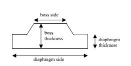
Figure5:Crosssectionofsquarediaphragmwitha squarecentralboss[5]
(Ramesh et al., 2015) performed an analysis using Multiphysics tool and the results showed that the capacitance sensitivity of normal diaphragm was 0.011pF/kPa and that of bossed diaphragm is 0.012pF/kPa.
(Yongtai He et al., 2012) presented a novel capacitive pressure sensor with the island-notch structure. The results showed that the linearity of the capacitive pressure sensor with island-notch structure reached up 0.9941 in the linear measurement zone, the sensitivity reached up 0.0019 pF/kPa, and the measurement range ofthesensorisalsoincreased.
Therefore for increased sensitivity and low nonlinearity bosseddiaphragmshouldbepreferred.
p-ISSN:2395-0072
There are two types of sensing structures available singleanddifferentialsensingstructures.
In single sensing structures there is only one capacitor involved in the sensing structurewhereas in differential sensing structure there are two capacitances involved. (Ettouhami et al., 2004) The differential sensing structurehashighersensitivitywhencomparedtosingle sidedstructure.Thenonlinearityerrorreducesfrom6.4 %to3.8%fordifferentialstructure.


Figure6:SingleSensingStructure


Figure7:DifferentialSensingStructure
(Achouch et al., 2020) designed a capacitive pressure sensor for large deflections. This work stated that the sensitivitywasincreasedfromaminimumof 9.98x10⁻² pF/hPa to a minimum of 3.4 x 10⁻¹ pF/hPa for differentialstructure.Thelinearitywasalsoimproved.
Table – 4: Singlev/sDifferentialStructure

International Research Journal of Engineering and Technology (IRJET) e-ISSN:2395-0056
Volume: 11 Issue: 05 | May 2024 www.irjet.net
The preference of the two structures depends on the application. For applications requiring higher sensitivity and where accurate pressure measurements are crucial thedifferentialstructureisgenerallypreferred.Whereas applicationswithmoderate pressureranges,wherehigh precision or sensitivity is not critical but manufacturing costisimportantthensinglesidedstructureispreferred.
(Bao et al., 2000) Electric excitation is necessary for sensingthecapacitance.Theexcitationvoltagegenerates an electrostatic force between electrodes of the capacitive sensor and which leads to the movement of the movable electrode. As a result the accuracy of the measurement of the pressure or even the normal operation of the capacitive sensor is affected by the excitation voltage. The discussion till 3.3 was based on single excitation mechanism. In single sided excitation the excitation voltage generates a force on the movable electrode. As a result this mechanism has a fixed offset displacementontheapplicationoftheelectricexcitation.
(Bao et al., 2000) On the other hand the double sided driving is used in differential capacitance structure. In thisexcitation mechanism boththesidesgenerate equal force on the movable electrode in opposite direction so there is no fixed offset. The linearity is better and the drivingvoltagescanbelargerwithoutcausingthepull-in effect.
Therefore in applications requiring higher sensitivity and lower nonlinearity with no offset displacement on the application of the excitation voltage, the differential structureispreferred.
In manufacturing of the capacitive pressure sensor anodic bonding is generally used. (Kárpáti et al., 2013) During this bonding 1000 V voltage is used for the bonding of the edges of the diaphragm to the substrate edges.(Baoetel.,2005)ontheapplicationofthevoltage, there is Force applied by the stationary electrode to the movableelectrodegivenby:
p-ISSN:2395-0072
(Wei et al., 2018) Pull-in effect is a common during anodic bonding. Anodic bonding is a key step in the fabrication process of capacitive sensors and actuators. So if the deformable electrode of the capacitor is forced by an electrostatic force due to the bonding voltage beyond the upper limit which is balanced by the mechanicalrestoringforce,itwillcomeintocontactwith a fixed electrode and remain attached even after the voltageisswitchedoff(seeFigure8)
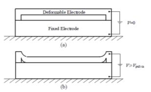
Figure 8: Pull in effect (a) Initial Structure without voltage bias and (b) attached structure with a voltage biasbeyondpull-involtage.
Thisisknownasthepull-ineffectandthecriticalvoltage is called pull-in voltage. The pull in voltage is given by equation(10)asin[1],[7]:
Where k is the mechanical elastic coefficient, d is the distance between the plates, A is the overlap area, is thepermittivityoffreespace.Formanufacturingprocess using anodic bonded for the capacitive sensors and actuatorsthepull-ineffectfrequentlyoccurs.Thispull-in effect occurs due to small gaps and large areas of capacitorplateswithdeformablefeaturesandextremely highbondingvoltagesbeingusedduringanodicbonding. To eliminate the pull in effect a capacitor is inserted in serieswiththemechanicalcapacitor.
As per mathematical calculations the pull in voltage is dependent on d and the mechanical elastic coefficient k sothevalueof d shouldbeselectedsuchthatthe
(V pull in) > (Voltage used in anodic bonding) (1000 V generally). Also the stable displacement of the movable electrodeinthenormaldirectionbyan externalagent is limited toonethirdoftheoriginal distance betweenthe twoplates.
After the manufacturing of the sensor die the readout circuithastobedesigned.Thechangeinthecapacitance hastobemeasuredandconvertedintoaquantitywhich canbeusedforfurtherprocessing.Thereforethechange in capacitance is converted to voltage. Different sensing mechanisms used for this conversion of the capacitance tovoltageareasfollows:
(i)DCBiassensingmethod

International Research Journal of Engineering and Technology (IRJET) e-ISSN:2395-0056
Volume: 11 Issue: 05 | May 2024 www.irjet.net p-ISSN:2395-0072

Figure9:DCbiassensingmethod[1]
TheDCbiassensingmethodhasaDCvoltageforbiasing the sensing capacitor. The DC bias sensing method is relatively simple to implement and does not require complexcircuitry.
(ii)Diodequadsensingmethod

Figure10:Diodequadsensingmethod[1]
In the diode quad sensing method, four diodes are arranged in a quad configuration. These diodes are typically connected in a bridge or diamond configuration,forminganetworkthatinterfaceswiththe capacitive sensor. The biasing voltage used in this is generally rectangular pulse. (Harrison et al., 1973) This method helps to isolate the sensor capacitance from the strayandcablecapacitance
(iii)Oppositedrivingsensingmethod
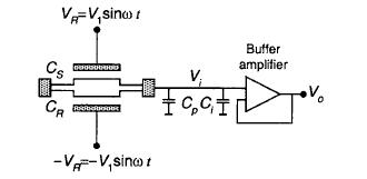
Figure11:Oppositedrivingsensingmethod[1]
The opposite driving sensing method is an effective technique for capacitive touch sensing systems, offering improved SNR, reduced parasitic effects, and enhanced sensitivityforreliableandaccuratetouchdetection.The sensing electrodes measure the differential capacitance changes induced by the application of the pressure. (Mohamed et al., 2015) By driving the electrodes in an opposite manner, common-mode noise and interference are minimized, improving the SNR of the measured signals. Opposite driving helps mitigate the effects of parasitic capacitance, stray capacitance, and environmental noise, leading to more accurate touch sensing
(iv)ForceBalancingEffect

Figure12:Forcebalancingsensingtechnique[1]
(Bao et al., 2005) In force balancing method the measurand is measured by the feedback voltage which creates an electrostatic force to balance the external force. This electrostatic force is in opposite direction to the external force and therefore keeps the central plate atthebalancedposition.
(v)Switchedcapacitorsensingmethod
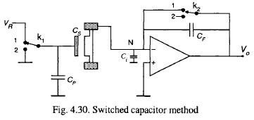
Figure13:Switchedcapacitorsensingmethod[1]
(Masahiro et al., 2003) The switched capacitor is based onthechargebalanceprinciple.Themajoradvantagesof this method are immunity to stray capacitance. This methodcanalsobeusedforoffsetcorrection.
Thereforeduetoreducedactiveandpassivecomponents in the circuit and immunity to stray capacitances the switchedcapacitorsensingmethodispreferred.
(Tsugai et al., 2003) developed a charge balanced capacitance to voltage converter for differential capacitor.Inthisthecircuitwasdevelopedusingopamp and switches using a new configuration for a switched capacitor type capacitance to voltage converter. The ideal results in this had 3.5 V and 4.5 V for the accelerationof4Gand8Grespectively.
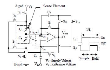
(a)Circuitconfiguration (b)Clocktimingdiagram
Figure14:ChargebalancedC-Vconverter

International Research Journal of Engineering and Technology (IRJET) e-ISSN:2395-0056
Volume: 11 Issue: 05 | May 2024 www.irjet.net p-ISSN:2395-0072
(Alam et al., 2010) proposed a design of capacitance to voltage circuit for pressure transducer as shown in Figure19.Inthisthedesignwasabletomeasureawide range of capacitance variations for the capacitive transducer. The designed circuit showed required performance parameters in terms of low power consumption, response and a linear output voltage. The circuit worked for a wide range of capacitance variation with a power supply voltage of 1.2 V. The capacitance was changed with 20fF steps in the simulation and the resultsshowedlinearoutputvoltagewithintherangeof 0.02-0.59Vforthevariationofthecapacitancefrom1001640fF,respectively.
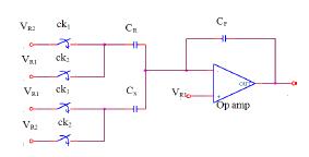
3.7 Parasitic Capacitances
Inthesensorvariouscapacitancesareintroduceddueto thedieandthereadoutcircuit.Inpracticalsituationsfor MEMS sensors the dimensions of the electrode are comparable to the distance between the electrodes. Therefore the capacitances cannot be approximated accurately as the edges of the electrodes have nonuniform electric field. As the electric field is present outside the sensor structure. This electric field leads to change in the capacitance. This effect is known as the fringe effect. Due to this effect the capacitance between the electrodes is larger than the nominal capacitance. Someexamplesareshownbelow

Figure16:Crosssectionofsometypicalcapacitive sensors[1]
At electrostatic level, the fringing phenomenon acts when an uneven charge distribution is present and the resulted effect is an exterior electrical field with bent field lines Due to this fringe effect the capacitance between the electrodes is larger than the nominal capacitancedue tothefringecapacitances.
Theparasiticcapacitancearealsogeneratedbetweenthe bonding area of the diaphragm and the substrate. This bondingareausuallyhasaninsulatorlayerdeposited.
TheparasiticcapacitancearealsointroducedbythePCB linkingtraces.
Theparasiticcapacitancearealsogeneratedbetweenthe top electrode and the ground and the bottom electrode andtheground.Thereadoutcircuitusedalsocontribute totheparasiticcapacitance.
3.7.1Methodstoavoidparasiticcapacitances
(Daul et al., 2021), (Islam et al., 2017) To avoid the inaccuracy in the calculation of the parallel plate capacitor due to the fringing fields at the edges of the electrodes, the guarding is necessary. Due to this guarding electrodes the electric field is inside the electrode area and therefore no fringe capacitance in includedinthenominalcapacitance.
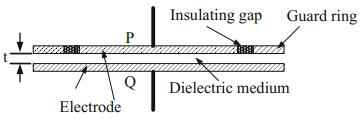
Figure17:Parallelplatecapacitorwithguardring[17]
ToavoidtheparasiticcapacitanceintroducedbythePCB linkingtracestwotracesoneinfrontoftheothercanbe positioned at the farther distance to avoid the mutual capacitancebetweenthetraces.
The readout circuit has intrinsic parasitic capacitance tolerance to avoid the parasitic capacitance due to the readoutcircuit.
(Nagatomoetal.,2018) Insertinglowdielectricconstant materials between the electrodes was reported to be effectivetoreducetheparasiticcapacitance.
(Pedersen et al., 2009) An on-chip CMOS ASIC for signal conditioninghelpsinavoidingwirebondsthatotherwise willinduceparasiticcapacitances.
(Pedersen et al., 2009) Another solution is to create a largercapacitivesignalbyfabricatinganarrayofsensing elements that are coupled in parallel, such that the total capacitance is the sum of all the single elements, thus makingtheparasiticcapacitancenegligible.
Undesired signals that do not carry any information is callednoise.Thenoiseplaysacrucialpartindesigningof acapacitivepressuresensorasthecapacitivesignalsare very small in magnitude. The noise interferes with the capacitance signal and distort the output. The different typesofnoisepresentinacapacitivepressuresensorare Thermalnoise,Flickernoiseandshotnoise.
Mechanical noise: (Utzetal.,2017)Thereisnoiseinthe die due to the Brownian motion of the particles inside the packaged sensor. Due to the thermal motion of the air atoms inside the MEMS package there is collision of theatomswiththesensorstructureleadingtonoise.

International Research Journal of Engineering and Technology (IRJET) e-ISSN:2395-0056
Volume: 11 Issue: 05 | May 2024 www.irjet.net p-ISSN:2395-0072
(Leland et al., 2005) derived the effect of the thermal noise on the MEMS gyroscopes. Therefore mechanical thermal noise is main source of noise other than the electricalnoise.
Imperfections in the semiconductor: Imperfections in the semiconductor used for manufacturing the sensor canalsoleadtonoise.
Thermal noise: The thermal noise is generally present at higher frequencies in the capacitive pressure sensor. (AlHinai et al., 2020) Thermal noise is one of the major sourcesofthenoisethatcanaffectthecapacitivesignals with low amplitude and comparable with the noise. The thermal noise is always present in the electrical equipment used in the circuit The vibration of charge carriers within an electrical conductor causes the thermal noise and it is directly proportional to the temperature,regardlessoftheappliedvoltage.
Flicker noise or 1/f noise: (AlHinaietal.,2020)Flicker noise or 1/f noise is a function of frequency, and its effects are often observed at low frequencies in electronic components used in the circuit. The random motion of the charge carriers leading to the charge carriers being randomly trapped and released between the interfaces of two materials results in flicker noise. Instrumentation amplifiers used to record electrical signals generally have flicker noise due to this phenomenon
Noise due to Power lines: (AlHinai et al., 2020) Power lines also introduces noise in the circuit. Power-line interference introduces 50–60 Hz frequency. This effect is due to the stray effect present in cables carrying signalsfromthesensortotheoutput.
EMI: There is also EMI (Electromagnetic Interference) present inside a capacitive pressure sensor due to the electricfieldoftheelectrodesofthesensor.Thiselectric field can be changed by any external electric field and thiscouldleadtochangeinthecapacitanceofthesensor.
Drift: Overtime,capacitivepressuresensorsmayexhibit drift, where the baseline capacitance or output signal gradually changes even in the absence of pressure variations.Driftcanbecausedbyfactorssuchasagingof components, material properties changes, or temperaturevariations.
Quantization noise: ( Utz et al., 2017) Some ASICs use directconversionofcapacitancechangetodigitalsignals. The direct conversion to digital signals from the capacitance leads to additional electrical and quantizationnoise.
3.8.1Methodstoreducenoise
The mechanical noise due to the air atoms inside the MEMS package can be reduced by vacuum sealing or electrostaticfeedback.
(AlHinai et al., 2020) Elimination of thermal noise is impossible; however, it can be reduced by reducing the temperature of operation or reducing the value of the resistanceinelectricalcircuits.
(AlHinai et al., 2020) Flicker noise can be effectively reduced by a technique called chopper stabilization or chopper,wheretheamplifieroffsetvoltageisreduced.In this chopper stabilization technique the signal is modulated twice using a square wave, first at the input and then at the output stage. So the signal is chopped twiceinthistechnique.
Different filtering techniques can be used to reduce the effectofPLIcorruptingthesignal.
TheEMIsourcescanaffectthecapacitanceofthesensor. So the sensor should be kept from EMI sources such as motors, power lines, and radio transmitters as far away aspossible
To prevent EMI the sensor is also generally shielded so that the external electric fields cannot change the capacitanceofthesensor.
Groundingprovidesapathfortheunwantednoisesignal to safely discharge to the ground. So it’s essential to groundthesensorandtheshieldatonepoint.Grounding will prevent creation of ground loops, which could inadvertentlyintroducemorenoise.
Choose components for the readout circuit with low noise and susceptibility to EMI. For example using opampwithin-builtoffsetandnoisecancellation.
(Eastsensor et al., 2024) Useshielded cablesto connect the pressure sensor, and avoid running these cables paralleltopowerlinesornearothersourcesofEMI.The shieldshouldalsobegroundedatoneendtoprovidean additionalpathforunwantedsignalstobedischarged.
There are different developed Application Specific Integrated Circuits available for the readout of the sensorsdeveloped.TheseASICscanbeusedaccordingto the application requirements. Most of these ASICs also convertthesensedparametertoaquantitywhichcanbe usedforfurtherprocessing.

International Research Journal of Engineering and Technology (IRJET) e-ISSN:2395-0056
Volume: 11 Issue: 05 | May 2024 www.irjet.net p-ISSN:2395-0072
Table – 5: DifferentASICsavailable[22–28]
Parameter
Type
to Digital Converter Configuration
Parasitic Capacitance Tolerance
400 pF (Shield for EMI also present) 50pF 4 pF (EMI resistance architecture) 10–80pF
Systemnoise floor: 0.3 pF at 100 sps (samplesper second)
10kHzto10 MHz (fsys/2 –fsys/16)kHz
Bandwidth 0.5–8kHz 8–87.2Hz 0 – 4 kHz Oscillator Frequency(1 –240kHz) External master clock input: 2 – 40 MHz

International Research Journal of Engineering and Technology (IRJET) e-ISSN:2395-0056
Volume: 11 Issue: 05 | May 2024 www.irjet.net p-ISSN:2395-0072
This paper presents a review of the capacitive pressure sensor. Differenttypeofsensorsavailablearecompared and analysed based on various properties showing that the capacitive pressure sensor should be preferred in applications requiring high sensitivity. This study also showed that the method involving application of the pressure normally and resulting in the displacement of themovableelectrodenormal tothefixed electrodeand decreasing the distance between the electrodes should be preferred for higher change in capacitance. The diaphragm having a square bossed structures has the lowestnonlinearity.Afterthestructuralanalysisthepull in effect was also analysed and the results showed that the diaphragm thickness and dimension of the sensor should be chosen such that the electrodes do not stick during the anodic bonding. Different capacitive sensing schemes are also shown in this paper. The parasitic capacitances introduced in the sensor due to various factors and the methods to avoid such capacitances are also explained in detail. The noise sources are also reviewed. A comparative analysis of the ASICs available fortheconversionofthecapacitancetovoltageordigital outputisalsopresented
References
[1] Minhang Bao-Analysis and Design Principles of MEMS Devices(2005)
[2] Balavalad, Kirankumar & Sheeparamatti, Basavaprabhu. (2015). A Critical Review of MEMS CapacitivePressureSensors.Sensors&Transducers. 187.120-128.
[3] Wikipedia contributors. (2023, November 16). Piezoresistive effect. InWikipedia, The Free Encyclopedia. Retrieved 11:29, March 31, 2024, from https://en.wikipedia.org/w/index.php?title=Piezor esistive_effect&oldid=1185443040
[4] Balavalad, Kirankumar & Sheeparamatti, Basavaprabhu. (2015). Sensitivity Analysis of MEMS Capacitive Pressure Sensor with Different Diaphragm Geometries for High Pressure Applications. International Journal of Engineering Research & Technology (IJERT). V4. 426-431. 10.17577/IJERTV4IS030671.
[5] Ettouhami, Aziz & Zahid, Noureddine & Elbelkacemi, Mourad. (2004). A novel capacitive pressure sensor structure with high sensitivity and quasi-linear response. Comptes Rendus Mecanique - C R MEC. 332.141-146.10.1016/j.crme.2003.10.001.
[6] Kárpáti, Tamás & Pap, Andrea & Kulinyi, Sándor. (2013).PrototypeMEMSCapacitivePressureSensor
Design and Manufacturing. Periodica Polytechnica ElectricalEngineering.57.3.10.3311/PPee.2066.
[7] Wei, Qiuxu & Xie, Bo & Lu, Yulan & Chen, Deyong & Chen, Jian & Wang, Junbo. (2018). An Analytical Method for Modelling Pull-In Effect during Anodic Bonding. Proceedings. 2. 969. 10.3390/proceedings2130969.
[8] Wikipedia contributors. (2024, January 17). Piezoelectric sensor. InWikipedia, The Free Encyclopedia. Retrieved 07:52, April 4,2024,from https://en.wikipedia.org/w/index.php?title =Piezoelectric_sensor&oldid=1196343314
[10]https://my.avnet.com/abacus/solutions/technologi es/sensors/pressure-sensors/coretechnologies/capacitive-vs-piezoresistive-vspiezoelectric/
[11] Meng Y, Chen G, Huang M. Piezoelectric Materials: Properties,Advancements,andDesignStrategiesfor High-Temperature Applications. Nanomaterials (Basel). 2022 Apr 1;12(7):1171. doi: 10.3390/nano12071171. PMID: 35407289; PMCID: PMC9000841.
[12]BernhardE.BoserUniversityofCalifornia,Berkeley boser@eecs.berkeley.edu. Capacitive Interface ElectronicsforSensingandActuation
[13]http://ecoursesonline.iasri.res.in/pluginfile.php/40 39/mod_resource/content/1/Lesson_17.htm
[14] M. Bao, H. Yin, H. Yang, S. Shen, Effects of electrostatic forces generated by the driving signal oncapacitivesensingdevices,SensorsandActuators A84(2000)213-219
[15] T. Pedersen, G. Fragiacomo, O. Hansen, E.V. Thomsen, Highly sensitive micromachined capacitive pressure sensor with reduced hysteresis andlowparasiticcapacitance,SensorsandActuators A:Physical,Volume154,Issue1,2009,Pages35-41, ISSN 0924-4247, https://doi.org/10.1016/j.sna.2009.07.013. (https://www.sciencedirect.com/science/article/pii/S092 4424709003379)
[16] Daul, L.; Jin, T.; Busch, I.; Koenders, L. Influence of GeometricPropertiesofCapacitiveSensorsonSlope Error and Nonlinearity of Displacement Measurements.Sensors2021,21, 4270. https://doi.org/10.3390/s21134270
[17] Islam, Tarikul. (2017). Advanced Interfacing Techniques for the Capacitive Sensors. 10.1007/978-3-319-55369-6_2.

International Research Journal of Engineering and Technology (IRJET) e-ISSN:2395-0056
[18] Nagatomo T, Miki N. Reduction of Parasitic Capacitance of A PDMS Capacitive Force Sensor. Micromachines (Basel). 2018 Nov 3;9(11):570. doi: 10.3390/mi9110570. PMID: 30715069; PMCID: PMC6266689.
[19] Harrison, D.R., & Dimeff, J. (1973). A Diode‐Quad Bridge Circuit for Use with Capacitance Transducers.Review of Scientific Instruments, 44, 1468-1472.
[20]Mohamed,M.G.A.,Kim,H.,&Cho,T.-W.(2015,April 25).AFastSensingMethodusingConcurrentDriving andSequential Sensingfor LargeCapacitanceTouch Screens.Journal of the Institute of Electronics and Information Engineers. The Institute of Electronics Engineers of Korea. https://doi.org/10.5573/ieie.2015.52.4.062
[21]Masahiro Tsugai,Yoshiaki Hirata,Toru Araki,Masafumi Kimata,A Charge Balanced C-V Converter for a Differential Capacitance Sensor,2003,123,9,p. 357362,2003/12/01,Online ISSN 1347-5525,Print ISSN 13418939,https://doi.org/10.1541/ieejsmas.123.357, htt ps://www.jstage.jst.go.jp/article/ieejsmas/123/9/123_9_ 357/_article/-char/ja,
[22] MicroSensors, Inc., 3001 Redhill Avenue, Costa Mesa, CA 92626, MS3110 Universal Capacitive ReadoutTMIC
[23] One Technology Way, P.O. Box 9106, Norwood, MA 02062-9106, U.S.A. Analog Devices, 24-Bit Capacitance-to-Digital Converter with Temperature Sensor
[24] Texas Instruments, Post Office Box 655303, Dallas, Texas 75265, FDC1004 4-Channel Capacitance-toDigital Converter for Capacitive Sensing Solutions, SNOSCY5B–AUGUST2014–REVISEDAPRIL2015
[25]AnalogMicroelectronicsGmbHAnderFahrt13,D –55124 Mainz, CAV444 Linear C/V-Converter for capacitiveinputsignals,May2014–Rev.3.0
[26] One Technology Way, P.O. Box 9106, Norwood, MA 02062-9106, U.S.A., Analog Devices, 12-Bit Capacitance-to-DigitalConverter
[27] Texas Instruments, Post Office Box 655303, Dallas, Texas 75265, FDC2112-Q1, FDC2114-Q1, FDC2212Q1, FDC2214-Q1 Multi-Channel 12-Bit or 28-Bit Capacitance-to-Digital Converter (FDC) for CapacitiveSensing,SNOSCZ9–MAY2016
[28] Renesas Electronics, ZSSC3123 cLiteTM Capacitive SensorSignalConditioner
Volume: 11 Issue: 05 | May 2024 www.irjet.net p-ISSN:2395-0072 © 2024, IRJET | Impact Factor value: 8.226 | ISO 9001:2008
[29]KimS-W,OhG-Y,LeeK-I,YangY-J,KoJ-B,KimY-W, Hong Y-S. A Highly Sensitive and Flexible Capacitive Pressure Sensor Based on Alignment Airgap Dielectric.Sensors. 2022; 22(19):7390. https://doi.org/10.3390/s22197390
[30] Li, We & jin, xin & Zheng, Yide & Chang, Xudong & Wang,Wenyu&Lin,Tong&Zheng,Fan&Onyilagha, Obiora&Zhu,Zhengtao.(2020).PorousandAirGap ElastomericDielectricLayerforWearableCapacitive Pressure Sensor with High Sensitivity and Wide DetectionRange.JournalofMaterialsChemistryC.8. 10.1039/D0TC00443J.
[31] AlHinai, Noura. (2020). Introduction to biomedical signal processing and artificial intelligence. 10.1016/B978-0-12-818946-7.00001-9.
[32]Oluwole,Leke&Olanipekun,Ayorinde&Ajide,O.O.. (2015). Design, construction and Testing of a strain gauge instrument. Int. J. Sci. Eng. Res. 6 1825-9. 6. 1825-1829.
[33] İRSEL, G. (2021, December 31). Research on electrical strain gages and experimental stress analysis: Case study for a full wheatstone bridge. DÜMF Mühendislik Dergisi, 783–792. https://doi.org/10.24012/dumf.1051434
[34]Zhu Jinget al2020J. Micromech. Microeng.30085012
[35] Hui Zhang, Nishuang Liu, Yuling Shi, Weijie Liu, YangYue,SiliangWang,YananMa,LiWen,LuyingLi, FeiLong,ZhengguangZou,andYihuaGao
ACS Applied Materials & Interfaces20168(34), 2237422381
DOI:10.1021/acsami.6b04971
[36] Tian, He & Shu, Yi & Wang, Xuefeng & Mohammad, Mohammad&Bie,Zhi&Xie,Qianyi&Lî,Chéng&Mi, Wentian & Yang, Yi & Ren, Tianling. (2015). A Graphene-Based Resistive Pressure Sensor with Record-High Sensitivity in a Wide Pressure Range. Scientificreports.5.8603.10.1038/srep08603.
[37]PangY,TianH,TaoL,LiY,WangX,DengN,YangY, Ren TL. Flexible, Highly Sensitive, and Wearable Pressure and Strain Sensors with Graphene Porous NetworkStructure.ACSApplMaterInterfaces.2016 Oct 12;8(40):26458-26462. doi: 10.1021/acsami.6b08172. Epub 2016 Oct 3. PMID: 27684520.
[38]Kim,YG.,Song,JH.,Hong,S.etal.Piezoelectricstrain sensor with high sensitivity and high stretchability

International Research Journal of Engineering and Technology (IRJET) e-ISSN:2395-0056
Volume: 11 Issue: 05 | May 2024 www.irjet.net p-ISSN:2395-0072
basedonkirigamidesigncutting.npjFlexElectron6, 52(2022). https://doi.org/10.1038/s41528-022-00186-4
[39]Z.H. Zhang,J. W. Kan,X.C.Yu,S. Y. Wang,J.J.Ma,Z. X. Cao; Sensitivity enhancement of piezoelectric force sensors by using multiple piezoelectric effects.AIP Advances1 July 2016; 6 (7): 075320. https://doi.org/10.1063/1.4960212
[40] Shaikh, M. Z. et al. “A Comparative Performance AnalysisOfCapacitive And PiezoresistiveMEMSFor PressureMeasurement.”(2008).
[41] G, shivaleela & J., Praveen & H N, Mahendra & G, Nithya. (2017). Comparative Study on Capacitive Pressure Sensor for Structural Health Monitoring ApplicationswithCoventorware.4.2641-2645.
[42] Lee, Y. S. and Kensall D. Wise. “A batch-fabricated silicon capacitive pressure transducer with low temperature sensitivity.”IEEE Transactions on ElectronDevices29(1982):42-48.
[43] S. Chaurasia, P. Sen and N. Bhat, "Using dielectric dropletstoimprovesensitivityofcapacitivesensors suitable for tactile sensing," 2017 IEEE 12th InternationalConferenceonNano/MicroEngineered and Molecular Systems (NEMS), Los Angeles, CA, USA, 2017, pp. 422-425, doi: 10.1109/NEMS.2017.8017056.
[44]Chhetry,Ashok &Yoon,Hyosang&Park,Jae-Yeong. (2017). A flexible and highly sensitive capacitive pressure sensor based on conductive fibers with a microporous dielectric for wearable electronics. J. Mater.Chem.C.5.10.1039/C7TC02926H.
[45]KimS-W,OhG-Y,LeeK-I,YangY-J,KoJ-B,KimY-W, Hong Y-S. A Highly Sensitive and Flexible Capacitive Pressure Sensor Based on Alignment Airgap Dielectric.Sensors. 2022; 22(19):7390. https://doi.org/10.3390/s22197390
[46] Young, Darrin & Du, Jiangang & Zorman, Christian. (2004). High-Temperature Single-Crystal 3C-SiC CapacitivePressureSensor.SensorsJournal,IEEE.4. 464-470.10.1109/JSEN.2004.830301.
[47] S. Saleh, A. Zaki, H. Elsemary and S. Ahmad, "Modeling of Sensitivity of fabricated Capacitive Pressure Sensor," IECON 2006 - 32nd Annual Conference on IEEE Industrial Electronics, Paris, France, 2006, pp. 3166-3169, doi: 10.1109/IECON.2006.347955.
[48] Chang, Sung-Pil & Allen, Mark. (2004). Capacitive pressuresensorswithstainlesssteeldiaphragmand substrate. J. Micromech. Microeng. 14. 612-618. 10.1088/0960-1317/14/4/023.
[49] T. Lahreche, M. Kandouci and Y. Hadjadj, "A Comparative Analysis of Different Diaphragm ShapedforMEMSCapacitivePressureSensor,"2022 19th International Multi-Conference on Systems, Signals&Devices(SSD),Sétif,Algeria,2022,pp.870874,doi:10.1109/SSD54932.2022.9955750.
[50] Roy, Priya & Chakraborty, Deborshi & Chattopadhyay, Madhurima. (2014). A Study of Silicon based MEMS Capacitive Sensor for Absolute Pressure Measurement of a Specific Range. InternationalJournalofComputerApplications.
[51] He, Yongtai & Liu, Jinhao & Lei, Li & He, Jinghong. (2012). A novel capacitive pressure sensor and interface circuitry. Microsystem Technologies. 19. 10.1007/s00542-012-1656-0.
[52] Ramesh, Akhil & Ramesh, P.. (2015). Trade-off between sensitivity and dynamic range in designing MEMS capacitive pressure sensor. 1-3. 10.1109/TENCON.2015.7372881.
[53] Achouch, S., Regragui, F., and Gharbi, M.: Improvement of the performance of a capacitive relative pressure sensor: case of large deflections, J. Sens. Sens. Syst., 9, 401–409, https://doi.org/10.5194/jsss-9-401-2020,2020.
[54] Leland, Robert. (2005). Mechanical-Thermal Noise inMEMSGyroscopes. SensorsJournal,IEEE.5.493500.10.1109/JSEN.2005.844538.
[55]Utz,Alexander&Walk,Christian&Haas,Norbert& Fedtschenko, Tatjana & Stanitzki, Alexander & Mokhtari, Mohammadreza & Goertz, M. & Kraft, Michael & Kokozinski, Rainer. (2017). An ultra-low noise capacitance to voltage converter for sensor applications in 0.35 µm CMOS. Journal of Sensors and Sensor Systems. 6. 285-301. 10.5194/jsss-6285-2017.
[56]Tsugai,Masahiro&Hirata,Yoshiaki&Araki,Toru& Kimata, Masafumi. (2003). A Charge Balanced CV Converter for a Differential Capacitance Sensor. Ieej Transactions on Sensors and Micromachines. 123. 357-362.10.1541/ieejsmas.123.357.
[57]Alam,A.H.M.&CheMustapha,NurulArfah&Sheroz, Khan & Islam, Md. (2010). Design of Capacitance to VoltageConverterforCapacitiveSensorTransducer. AmericanJournalofAppliedSciences.7.
[58] Eastsensor. (2024, April 8). Pressure sensor noise and EMI. Retrieved from https://www.eastsensor.com/blog/pressuresensor-noise-and-emi/
© 2024, IRJET | Impact Factor value: 8.226 | ISO 9001:2008
|