International Research Journal of Engineering and Technology (IRJET) e-ISSN: 2395-0056
Volume: 12 Issue: 03 | Mar 2025 www.irjet.net p-ISSN: 2395-0072


International Research Journal of Engineering and Technology (IRJET) e-ISSN: 2395-0056
Volume: 12 Issue: 03 | Mar 2025 www.irjet.net p-ISSN: 2395-0072
Mr.A.Marimuthu, Rithanya P, Saarika K, Sharmitha M
Department of Electrical and Electronics Engineering, K.L.N. College of Engineering, Pottapalayam, Sivagangai District.
Abstract - TheZVZCSthree-levelDC/DCconverterenhances efficiency by addressing the limitations of traditional ZVS converters. While ZVS reduces voltage-related switching losses, it struggles with circulating energy losses, parasitic ringing,andalimitedZVSrange.Toovercometheseissues, the ZVZCS converter incorporates an auxiliary circuit and phaseshiftcontrol.ThisallowsouterswitchestoachieveZVS, minimizing voltage-related losses, while inner switches operate under ZCS, ensuring they turn on and off at zero current, eliminating current-related losses. This approach suppressesparasiticringing,reducesenergydissipation,and extendstheZVSrangeacrossvaryingloads,improvingoverall performance.Alamploadisusedtoevaluateitsstabilityand powerdelivery.Byenhancingpowerefficiency,stability,and thermalmanagement,theZVZCSconverterisidealforhighpower applications such as renewable energy systems, electric vehicles, and industrial power supplies, ensuring optimal energy conversion with minimal losses and improvedsystemreliability.
Key words Zero Voltage Switching, Zero Current Switching, Three level DC-DC converter, Circulating energy losses,Parasiticringing,Phaseshiftcontrol,Highefficiency, Loadrange,HighpowerDC-DCconversion.
Zero Voltage Switching (ZVS) and Zero Current Switching(ZCS)aretwoessentialtechniquesusedinpower electronics to improve the efficiency of power conversion systems by minimizing switching losses. In conventional switching, when a power switch such as a transistor or a MOSFETturnsonoroff,thereisanoverlapbetweenvoltage andcurrent.Thisoverlapresultsinenergydissipationinthe form of heat, reducing overall system efficiency and increasingthermalstressonthecomponents.ZVSandZCS are designed to eliminate or significantly reduce these switching losses by ensuring that the switch transitions occuratspecificmomentswheneithervoltageorcurrentis zero,therebypreventingunnecessarypowerdissipation.
ZeroVoltageSwitching(ZVS)isatechniquewhere the power switch is turned on when the voltage across it reaches zero. This is typically achieved using a resonant circuitconsistingofaninductorandacapacitor(L-Ccircuit). Theresonantcircuitallowsthevoltageacrosstheswitchto oscillate naturally, and the switch is turned on precisely
whenthevoltageiszero.Bydoingso,theenergystoredin the circuit components is used efficiently, and the power losses that would otherwise occur due to capacitive dischargeareminimized.ZVSisparticularlyusefulinhighfrequency power conversion applications, such as in softswitching power supplies, where it helps to reduce electromagneticinterference(EMI)andswitchingstresson components. The technique is widely used in resonant inverters,inductionheatingsystems,andhigh-frequencyDCDCconverters,wherereducingswitchinglossesiscriticalto improvingoverallefficiency.
Zero Current Switching (ZCS), on the other hand, focusesonensuringthattheswitchtransitionsoccurwhen the current flowing through it is zero. This technique is particularly beneficial in circuits where high currents are involved,asitpreventsthepowerswitchfromexperiencing high current surges during switching operations. When a switch turns off while current is still flowing, the sudden interruption leads to energy dissipation and can cause voltagespikesduetocircuitinductance,whichmaydamage the switch or require additional snubber circuits. ZCS eliminates this issue by ensuring that the switch turns off onlywhenthecurrenthasnaturallydecreasedtozero.This reduces the stress on the switch and lowers energy dissipation,improvingsystemreliabilityandextendingthe lifespan of power devices. ZCS is commonly used in highpowerconverters,resonantconverters,andcircuitswhere inductiveloadsarepresent.
By employing ZVS and ZCS, power electronics designerscanachievesignificantimprovementsinsystem efficiency. Reduced switching losses mean less wasted energy,whichdirectlytranslatesintocostsavingsandlower operationalexpensesoverthelifetimeofaproduct.
Additionally,minimizingswitchinglossesreduces heatgeneration,whichisacriticalfactorinpowerelectronic design. Excess heat often necessitates additional cooling mechanisms, such as heatsinks, fans, or liquid cooling systems,whichincreaseboththesizeandcostoftheoverall system. WithZVSandZCS,theneedfor extensivethermal managementisminimized,makingpowerelectronicdesigns more compact, lightweight, and cost-effective. This is particularly beneficial in applications where space and weight are constraints, such as in electric vehicles, solar inverters,andportableelectronicdevices.

International Research Journal of Engineering and Technology (IRJET) e-ISSN: 2395-0056
Volume: 12 Issue: 03 | Mar 2025 www.irjet.net p-ISSN: 2395-0072
The importance of ZVS and ZCS extends beyond efficiency and cost savings. By reducing switching losses, these techniques also help in lowering electromagnetic interference,whichiscrucialforensuringcompliancewith electromagnetic compatibility (EMC) standards in modern electronicsystems.Furthermore,improvedefficiencyleadsto better system reliability, as components experience less thermalandelectricalstress.
Aspowerelectronicstechnologycontinuestoevolve, theadoptionofZVSandZCSisexpectedtoremainacrucial aspectofdesigninghigh-performanceand energy-efficient powerconversionsystems.Thesetechniquesarewidelyused invariousapplications,includingrenewableenergysystems, industrialmotordrives,powersupplies,andelectricvehicle charging infrastructure. With ongoing advancements in semiconductor technology and circuit design, ZVS and ZCS will continue to play a key role in optimizing power conversion efficiency and enhancing the performance of powerelectronicdevices.
2.1. INTRODUCTION TO HARDWARE SWITCHING
Hardwareswitchingisafundamentaltechniquein power electronics that uses semiconductor devices like MOSFETstoregulateelectricalpowerbyswitchingbetween "on"and"off"states.Thismethodiswidelyappliedinpower supplies, motor drives, and renewable energy systems. MOSFETs are favoured due to their fast switching capabilities,allowingefficientpowertransferwithminimal resistancewhenturnedonandblockingcurrentflowwhen turned off. However, switching introduces challenges that impactefficiencyandreliability.
2.2. SWITCHING LOSSES AND THERMAL MANAGEMENT
Oneof thekey concernsin hardwareswitching is switchinglosses,whichoccurduetotheoverlapofvoltage and current during transitions. Ideally, MOSFETs should switchinstantaneously,butinreality,thereisalwaysabrief periodwherebothvoltageandcurrentexistsimultaneously, leadingtopowerdissipation.Thisresultsinheatgeneration, which must be managed to prevent damage and maintain systemefficiency.Effectivethermalmanagementstrategies suchasheatsinks,coolingfans,andoptimizedcircuitdesign helpmitigatetheseeffects.
2.3. PARASITIC RINGING AND ELECTROMAGNETIC INTERFERENCE (EMI)
Parasitic ringing arises due to the interaction between stray inductance and capacitance in the circuit, causing oscillations during switching. These oscillations generate high-frequency noise, voltage spikes, and electromagnetic interference (EMI), which can disrupt circuit operation and damage components like rectifier diodes. To counteract these effects, designers implement
techniquessuchassnubbercircuitstoabsorbexcessenergy, smoothwaveforms,andreduceoscillations.
2.4 ZERO VOLTAGE SWITCHING FOR EFFICIENCY IMPROVEMENT
To enhance efficiency and minimize switching losses, power electronics designers use Zero Voltage Switching(ZVS).This technique ensuresthat the MOSFET switcheswhenthevoltageacrossitisnearlyzero,reducing energy dissipation. Achieving ZVS requires the use of resonant circuits consisting of inductors and capacitors, which create favourable conditions for zero-voltage transitions. Proper timing of switching events allows MOSFETs to turn on and off optimally, reducing heat generationandimprovingoverallefficiency.
The proposed methodology significantly enhances power conversion efficiency by incorporating phase shift controlandaflyingcapacitorintheprimarysideofaDC-DC converter.Thisinnovativeapproachisdesignedtominimize switchinglosses,improveenergytransfer,andoptimizethe overallperformanceofpowerelectronicsystems.Bycarefully regulating the timing of switch transitions, this method ensuressmootherpowerflow,reducingabruptchangesthat couldleadtounnecessarypower dissipationand excessive stressoncircuitcomponents.Additionally,inthisproposed methodology,wehaveincorporatedalamploadastheoutput, further demonstrating the system’s capability to handle practicalloadconditionseffectively.
Phase shift control is a modulation technique that introducesacontrolleddelaybetweentheswitchingsignalsof theprimary-sidetransistorsinapowerconverter.Insteadof switching all transistors simultaneously, a phase shift is applied between them, allowing energy transfer to be managedina controlledand gradual manner.Thismethod minimizestheoverlapbetweenvoltageandcurrent,whichis a major source of switching losses in conventional hardswitchingsystems.Byreducingthesimultaneousoccurrence ofhighvoltageandcurrent,phaseshiftcontrolsignificantly decreasesheatgeneration,leadingtoimprovedefficiencyand alongerlifespanforpowercomponents.
Acriticalcomponentofthismethodologyistheflying capacitor,whichdynamicallybalancesvoltageacrossvarious circuit elements. Unlike a conventional capacitor that maintains a fixed voltage level, a flying capacitor shifts its voltageinresponsetocircuitconditions.Thisabilitytofloat between different voltage levels helps to prevent excessive voltagespikes,whichcanotherwisedegradesystemreliability and cause power dissipation. The flying capacitor ensures voltagebalancewithinthecircuit,leadingtoimprovedpower regulationandincreasedstability.

International Research Journal of Engineering and Technology (IRJET) e-ISSN: 2395-0056
Volume: 12 Issue: 03 | Mar 2025 www.irjet.net p-ISSN: 2395-0072
Inadditiontomaintainingvoltagebalance,theflying capacitorassistsinachievingZeroVoltageSwitching(ZVS) fortheouterswitchesinthecircuit.ZVSisatechniquethat allowsswitchestoturnonwhenthevoltageacrossthemis nearly zero, thereby minimizing switching losses. This approachisparticularlybeneficialinhigh-frequencypower conversion applications, where conventional switching methodsoftenleadtoexcessivelossesandincreasedthermal dissipation. By utilizing ZVS, the proposed methodology reducestheenergylostduringswitchingtransitions,thereby enhancingefficiencyandreducingstressonsemiconductor devices.Thelowerstressoncomponentsultimatelyimproves the durability and performance of the power electronics system.
Additionally, this methodology incorporates Zero CurrentSwitching(ZCS)tooptimizeturn-offtransitions.ZCS ensures that switches turn off when the current flowing through them is zero, eliminating the energy dissipation typically associated with turn-off events in traditional switchingtechniques.Thisisparticularlyusefulinreducing conduction losses and preventing unwanted oscillations or voltage spikes, which could lead to electromagnetic interference(EMI).ThecombinedimplementationofZVSand ZCSenablesanefficientsoft-switchingenvironment,where voltageandcurrent-relatedswitchinglossesaresignificantly minimized.
By integrating phase shift control, flying capacitor balancing, and advanced soft-switching techniques, this methodologyeffectivelyaddresseskeychallengesinmodern powerelectronics.Theproposedapproachleadstosignificant improvements in power conversion efficiency, enhances systemreliability,andreducesthermalstress.Asaresult,itis highly suitable for high-performance applications such as renewable energy systems, electric vehicles, and nextgeneration power supplies. This innovative technique ensures better energy management while maintaining operationalstability,makingitapracticalandefficientpower conversion strategy for future power electronics advancements.Furthermore,theinclusionofalamploadas theoutputvalidates the system’sabilitytodrive real-world loads,makingitarobustandadaptablesolutionforvarious powerconversionapplications.
The proposed methodology aims to enhance the powerconversionefficiencyandreduceswitchinglossesin DC-DCconvertersbyintegratingphaseshiftcontrolwitha flying capacitor. This approach addresses the inherent challenges in power electronic systems, such as energy dissipation,voltagefluctuations,andswitchinglosses,which can degrade overall system performance and reliability. By employingacombinationofphaseshiftcontrolandaflying capacitor, the methodology optimizes energy transfer,
minimizes stress on circuit components, and improves operationalefficiency.
Phaseshiftcontrolplaysacriticalroleinrefiningthe timingofswitchingtransitionswithintheconverter.Instead of conventional hard-switching techniques, which lead to abrupt voltage and current changes, phase shift control introduces a deliberate phase shift between the switching signals of primary-side switches. This controlled timing facilitates smooth transitions between switching states, reducing power dissipation and component stress. As a result, the converter operates with lower electromagnetic interference (EMI) and improved thermal performance, leadingtoenhancedlongevityandreliabilityofthecircuit.A keycomponentintheproposeddesignistheflyingcapacitor, whichdynamicallybalancesvoltageacrossdifferentcircuit elements. In high-frequency power conversion systems, sudden voltage spikes can compromise the integrity of semiconductordevicesandpassivecomponents.Theflying capacitor effectively mitigates these voltage spikes by redistributingchargewithinthecircuit,preventingexcessive voltagedifferentialsthatcouldotherwiseleadtocomponent failure. This voltage regulation function is crucial in maintainingsteadyandefficientpowerconversion.
Anothersignificantadvantageofintegratingaflying capacitorisitsroleinachievingZeroVoltageSwitching(ZVS) and Zero Current Switching (ZCS). ZVS ensures that outer switches in the converter turn on at nearly zero voltage, significantly reducing turn-on losses. This technique is particularly effective in soft-switching topologies, where it minimizesenergy dissipationduringswitchingtransitions. Meanwhile,ZCSenablesswitchestotransitionatzerocurrent, reducing turn-off losses by preventing abrupt current interruptions that can cause voltage spikes and energy dissipation.Together,ZVSandZCSenhancetheefficiencyof the power conversion process, contributing to reduced thermalstressandimprovedoverallperformance.
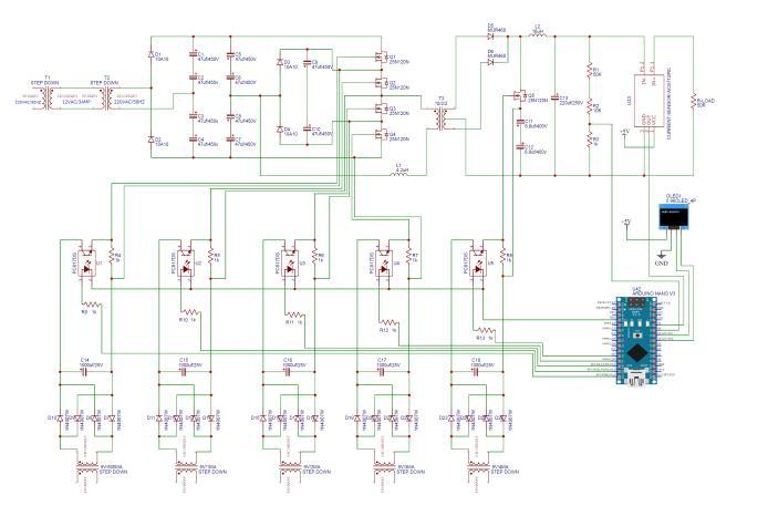
Toensurereal-timemonitoringandadaptivecontrol oftheconverter’sperformance,anArduinomicrocontrolleris integratedintothesystem.TheArduinoprocessesdatafrom an ACS712 current sensor module and a voltage divider circuittocontinuouslymeasurecurrentandvoltagevalues. The ACS712 module provides precise current sensing by leveragingtheHalleffectprinciple,whilethevoltagedivider circuitallowssafemeasurementofvoltagelevelsbyscaling down higher voltages to a readable range for the microcontroller.ThecollecteddataisdisplayedonanOLED screen,providingreal-timefeedbackonvoltageandcurrent values. This real-time visualization aids in monitoring the converter’s operational parameters, ensuring it functions withindefinedperformancelimits.Thefeedbackmechanism allowsforquickadjustmentstooptimizeefficiency,prevent overloading, and enhance overall system reliability. In the integration of phase shift control with a flying capacitor presents a robust solution for improving DC-DC converter

International Research Journal of Engineering and Technology (IRJET) e-ISSN: 2395-0056
Volume: 12 Issue: 03 | Mar 2025 www.irjet.net p-ISSN: 2395-0072
performance.Byoptimizingswitchingtransitions,reducing voltagespikes,andimplementingreal-timemonitoring,this methodology enhances efficiency, minimizes power losses, and ensures reliable operation of the power conversion system.
Thethree-levelDC-DCconverteroperatesinthreekeystages:
1. DCtoACConversionandSwitchingOptimization
2. ACProcessingandDCOutputStabilization
3. Real-TimeMonitoringandPerformanceOptimization

5.1. DC to AC Conversion and Switching Optimization:
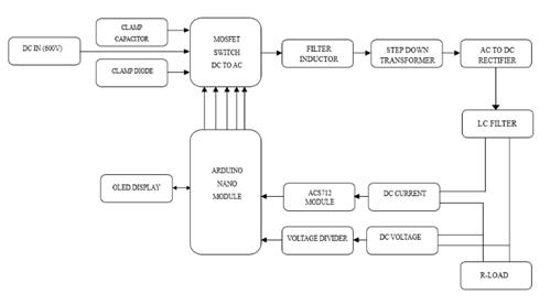
Thethree-levelDC-DCconverterbeginsitsoperation witha high-voltageDCinput,typicallyaround600V,which serves as the primary power source. This high voltage ensures efficient power transfer and is essential for applicationsrequiringsubstantialenergyconversion,suchas industrialpower supplies, electric vehicles, and renewable energysystems.However,workingwithsuchhighvoltages introduces challenges like excessive stress on switching components,potentialvoltagespikes,andsignificantpower dissipation.Tomitigatetheseissues,aclampcapacitoranda clamp diode are incorporated into the system. The clamp capacitor plays a crucial role in voltage balancing by distributingthevoltageevenlyacrosstheMOSFETswitches, whiletheclampdiodehelpsinsuppressingtransientvoltage spikesthatoccurduringswitchingoperations.Withoutthese components, MOSFETs would experience uneven voltage stress,leadingtoreducedreliabilityandpotentialfailureover time.
The primary function of the MOSFETs in this converteristoperformhigh-frequencyswitching,converting the DC input into an AC signal. This alternating signal is necessaryforfurtherprocessing,asitallowsefficientvoltage transformationandconditioningbeforebeingconvertedback into a regulated DC output. Traditional power converters suffer from substantial switching losses due to abrupt
changes in voltage and current during transitions. These lossesgenerateexcessheat,reducingoverallefficiencyand increasingcoolingrequirements.Toaddressthis,thesystem employs Zero Voltage Switching (ZVS) and Zero Current Switching(ZCS)techniques,whichsignificantlyoptimizethe switchingprocess.ZVSensuresthatswitchingoccurswhen the voltage across the MOSFETs is zero, effectively eliminatingcapacitivedischargelosses.Thisisachievedby carefully timing the switching events so that the voltage naturallyreacheszerobeforetheswitchturnsonoroff.By doing so, the system prevents energy stored in parasitic capacitances from being dissipated as heat. On the other hand, ZCS ensures that switching takes place when the current through the MOSFETs is zero, minimizing energy losses caused by inductor currents. This is particularly importantincircuitswithhighinductance,whereswitching at non-zero current levels can lead to excessive energy dissipation. The combination of ZVS and ZCS greatly enhances efficiency by reducing both voltage and currentrelated switching losses. This not only improves power conversion efficiency but also lowers heat generation, reducing the need for additional cooling mechanisms. Furthermore, by minimizing stress on the switching components, the lifespan of MOSFETs and other semiconductordevicesisextended,reducingmaintenancecosts andenhancingoverallsystemreliability.
Oncethehigh-voltageDCinputhasbeensuccessfully convertedintoanalternatingsignal,itmustundergofurther processingtoensureastableandwell-regulatedoutput.The firststageinthisprocessispassingtheACsignalthrougha filterinductor.Thisinductorplaysacriticalroleineliminating high-frequency noise and unwanted distortions that may arise due to rapid switching transitions. If left unfiltered, thesehigh-frequencycomponentscancauseelectromagnetic interference (EMI) and affect the performance of other electronicdevices.By smoothing out theAC waveform, the filter inductor ensures cleaner power transmission. After filtering,theACsignalisfedintoastep-downtransformer, which adjusts the voltage level based on the specific requirementsoftheconnectedload.Thetransformeroperates on the principle of electromagnetic induction, where the primarywindingreceivesthealternatingsignal,inducinga correspondingvoltageinthesecondarywinding.Theturns ratioofthetransformerdetermineshowmuchthevoltageis reduced, ensuring that the output is suitable for further rectificationanduse.
This step is particularly important in applications wheretheinitialhigh-voltageDCmustbeconvertedintoa lowervoltageforsafeoperation,suchasinbatterycharging orelectronicdevicepowersupplies.Sincethefinaloutputof the system needs to be DC, the stepped-down AC signal undergoesrectificationusinganACtoDCrectifier.

International Research Journal of Engineering and Technology (IRJET) e-ISSN: 2395-0056
Volume: 12 Issue: 03 | Mar 2025 www.irjet.net p-ISSN: 2395-0072
The rectifier consists of diodesoractiveswitching componentsthatallowcurrenttoflowinonlyonedirection, converting the bidirectional AC waveform into a unidirectional DC signal. However, even after rectification, someACrippleremainsintheoutput,whichcanaffectthe performanceofsensitiveelectroniccircuits.Tofurtherrefine theoutput,anLCfilterisemployed. TheLCfilter,composed ofaninductorandacapacitor,isdesignedtosmoothoutany remainingvoltagefluctuations,ensuringacleanandstableDC output.TheinductorintheLCfilterpreventssuddencurrent changes, while the capacitor absorbs high-frequency variations, providing a continuous DC supply to the connected load. This filtering process is crucial for maintainingpowerquality,asexcessive voltage fluctuations canleadtounstableperformanceorevendamagetoelectronic components. Once the filtering is complete, the final DC output is delivered to the resistive load (R-Load), representingtheapplicationwheretheconvertedpoweris utilized.
Toensureoptimalefficiency,stability,andsafety,the three- level DC-DC converter is equipped with an Arduino Nano microcontroller, which acts as the control and monitoringunit.TheprimaryfunctionoftheArduinoisto managetheMOSFETswitchingsequences,ensuringthatZVS andZCStechniquesareimplementedcorrectlyformaximum efficiency.Inadditiontocontrollingswitchingoperations,the Arduino continuously collects real-time data from various sensors to monitor the system’s performance and adjust parametersasneeded.Oneofthekeysensorsintegratedinto the system is the ACS712 current sensor module, which providescontinuousmeasurementsoftheDCcurrentflowing through the circuit. This data is crucial for detecting overcurrent conditions, which could indicate excessive load demandorfaultswithinthesystem.Ifanovercurrentsituation is detected, the Arduino can trigger protective mechanisms such as shutting down the circuit or adjusting switching patternstopreventdamage.
To ensure accurate voltage monitoring, a voltage dividercircuitisusedtostepdownhigh-voltagesignalstoa safe range that the Arduino can process. Since the microcontroller operates at lower voltage levels, direct measurement of high- voltage signals is not possible. The voltagedividerreducesthesesignalsproportionally,allowing theArduinotoprocess and analyze voltage fluctuations in real-time. Once theArduino processesthe collecteddata, it displays key system parameters on an OLED screen. This real-time display provides essential information such as voltage levels, current flow, and switching states, allowing users to monitor performance and make necessary adjustmentsforimprovedoperation.Theabilitytovisualize real-timedataenhancestroubleshootingcapabilities,making iteasiertoidentifyandresolvepotentialissuesbeforethey impact system performance By integrating real-time
monitoringandcontrol,the system ensureshighefficiency, reducedenergylosses,andenhancedreliability.Inrenewable energyapplications,suchassolarandwindpowersystems, the converter plays a crucial role in stepping down and regulatingpowerfromhigh-voltagesourcestousablelevels.In electric vehicles,itis usedfor efficient batterychargingand energy distribution. Similarly, industrial automation and telecommunicationsrelyonsuchconverterstoprovidestable DCpowerforcriticalequipment.Theaerospacesectorbenefits from the system’s high efficiency and reliability, making it suitableformission-criticalpowermanagementapplications.
Overall,thethree-levelDC-DCconverterwithZVSand ZCS techniques represents a highly efficient, reliable, and intelligentpowerconversionsolution.Bycombiningoptimized switching methods, advanced voltage balancing, effective filtering, and real-time monitoring, this system achieves superiorperformancewithminimalenergylosses.

The integration of an Arduino-based control mechanismfurtherenhancesitsadaptability,ensuringstable operation across various applications. As power electronics continuetoevolve,suchadvancedconverterswillplayacrucial roleindevelopingnext-generationenergy-efficientsystems.
Thethree-levelDC-DCconverterwithZeroVoltage Switching (ZVS) and Zero Current Switching (ZCS) techniques represents a pinnacle in efficient power conversiontechnology.Thissophisticatedconvertersystemis designedtohandlehigh-voltageDCinputs,typicallyaround 600V, and efficiently transform them into regulated DC outputswithminimalenergylossandheatgeneration.This makes it highly suitable for applications that require substantial energy conversion, such as industrial power supplies,electricvehicles,andrenewableenergysystems.One of the key challenges in high-voltage power conversion is managing the excessive stress on switching components, potentialvoltagespikes,andsignificantpowerdissipation.To address these issues, the converter incorporates a clamp

Volume: 12 Issue: 03 | Mar 2025 www.irjet.net p-ISSN: 2395-0072
capacitor and a clamp diode. The clamp capacitor plays a crucial role in voltage balancing by distributing the voltage evenly across the MOSFET switches. This ensures that no single MOSFET experiences undue stress, which could otherwiseleadtoreducedreliabilityandpotentialfailureover time.Theclampdiodehelpssuppresstransientvoltagespikes that occur during switching operations, protecting the MOSFETsfromdamageandenhancingtheoveralldurability and efficiency of the system. The primary function of the MOSFETs in this converter is to perform high-frequency switching, converting the DC input into an AC signal. This alternating signal is necessary for further processing, allowing efficient voltage transformation and conditioning before being converted back into a regulated DC output. Traditional powerconvertersoften suffer from substantial switchinglossesduetoabruptchangesinvoltageandcurrent during transitions, generating excess heat and reducing overall efficiency. To optimize the switching process, the converteremploysZVSandZCStechniques.ZVSensuresthat switching occurs when the voltage across the MOSFETs is zero,effectivelyeliminatingcapacitivedischargelosses.This isachievedbytimingtheswitchingeventssothatthevoltage naturallyreacheszerobeforetheswitchturnsonoroff.By doing so, the system prevents energy stored in parasitic capacitancesfrombeingdissipatedasheat.ZCS,ontheother hand, ensures that switchingtakes place when the current through the MOSFETs is zero, minimizing energy losses causedbyinductorcurrents.Thisisparticularlyimportantin circuitswithhighinductance,whereswitchingatnon-zero currentlevelscanleadtoexcessiveenergydissipation.The combinationofZVSandZCSgreatlyenhancesefficiencyby reducingbothvoltageandcurrent-relatedswitchinglosses. Thisnotonlyimprovespowerconversionefficiencybutalso lowers heat generation, reducing the need for additional coolingmechanisms.Furthermore,byminimizingstresson the switching components, the lifespan of MOSFETs and other semiconductor devices is extended, reducing maintenancecostsandenhancingoverallsystemreliability. TheACprocessingstageoftheconverterinvolvesfiltering, step-downtransformation,andrectificationtoensureastable andripple-freeDCoutput.TheLCfilterplaysacrucialrolein smoothing voltagefluctuations,makingthesystemsuitable for applications requiring precise power regulation. Realtimemonitoringandcontrol,facilitatedbyanArduinoNano microcontroller, significantly enhance the system’s adaptability.Continuousvoltageandcurrentmeasurements, combined with OLED-based visual feedback, allow for dynamicadjustments,ensuringoptimalperformanceunder varying load conditions. The integration of protective features, such as overcurrent detection, further improves systemsafetyandlongevity.Thisconverter’sabilitytodeliver highefficiency,real-timeadaptability,andreliableoperation makesitidealformodernpowerapplications.Asindustries continue to demand energy-efficient solutions, this technologywillplayavitalroleinshapingthefutureofpower electronics, ensuring sustainable and optimized energy utilization across various sectors, including aerospace,
telecommunications,andindustrialautomation.Throughthe effective management of high voltages and the implementationofadvancedswitchingtechniques,thethreelevelDC-DCconverterachievessuperiorperformancewith minimalenergylosses,positioningitasacornerstoneofnextgenerationpowerelectronics.
SDG Goal 7: Affordable and Clean Energy by promoting efficient energy use and advancing sustainable powerelectronics.
SDG Goal 8: Decent Work and Economic Growth by fostering innovation in power electronics, reducing energy costs,andpromotingsustainableindustrialproductivity.
SDG Goal 9: Industry, Innovation, and Infrastructure by supportingsustainableindustrialgrowth,improvingenergy efficiency,andfosteringinnovationinpowerelectronics.
[1] Zhiliang Zhang, Xinbo Ruan, “Full-bridge Three-Level Converter with the Flying Capacitor and Two Clamping Diodes, in: 2005” IEEE 36th power electronics specialists conference,2005,pp.425–430.
[2]Guo,Z.;Sun,K.;Sha,D.ImprovedZVSthree-levelDC–DC converter withreducedcirculatingloss.IEEETrans.Power Electron.2016.
[3] M. Pahlevani and P. K. Jain, ‘‘Soft-switching power electronics technology for electric vehicles: A technology review,’’IEEEJ.Emerg.Sel.TopicsInd.Electron.,vol.1,no.1, pp.80–90,Jul.2020.
[4]R.FarajiandH.Farzanehfard,‘‘Fullysoftswitchedmultiport DC-DC converter with high integration,’’ IEEE Trans. PowerElectron.,vol.36,no.2,pp.1901–1908,Feb.2020.
[5] R. Faraji, H. Farzanehfard, M. Esteki, and S. Ali Khajehoddin, ‘‘A lossless passive snubber circuit for threeport DC–DC converter,’’ IEEE J. Emerg. Sel. Topics Power Electron.,vol.9,no.2,pp.1905–1914,Apr.2021.
[6]S.S.Dobakhshari,S.H.Fathi,andJ.Milimonfared,‘‘Anew soft-switchedthree-portDC/DCconverterwithhighvoltage gain and reduced number of semiconductors for hybrid energyapplications,’’IEEETrans.PowerElectron.,vol.35,no. 4,pp.3590–3600,Apr.2020.
[7] Shi, Y.; Yang, X. Wide-range soft-switching PWM threelevel combined DC–DC converter without added primary clampingdevices.IEEETrans.PowerElectron.2014.