International Research Journal of Engineering and Technology (IRJET)
e-ISSN: 2395-0056
Volume: 12 Issue: 03 | Mar 2025
p-ISSN: 2395-0072
www.irjet.net
DESIGN AND ANALYSIS OF INTERLEAVED BOOST CONVERTER FOR EV BATTERY CHARGING APPLICATION Lokeshan B 1, Logeshkumar S 2, Dinesh B 3, Mr.A.Marimuthu 4 ,Dr.S.Venkatesan 5 1,2,3Student, Dept. of Electrical & Electronics Engineering, K.L.N. college, Tamil Nadu, India
4,5 Professor, Dept. of Electrical & Electronics Engineering, K.L.N. college, Tamil Nadu, India ---------------------------------------------------------------------***--------------------------------------------------------------------its low conduction loss, high voltage step-up, reduced Abstract - This paper presents the design and analysis of
output voltage ripple, and faster transient response. Although IBC requires more inductors, increasing complexity compared to a conventional boost converter, it is preferred due to low ripple at both input and output. To reduce this complexity, a coupled IBC is considered. The proposed topology employs a Hill Climbing MPPT algorithm for better control and optimal energy harnessing. The IBC topology enhances output power with high efficiency, and steady-state voltage ripples at the output capacitors are minimized. The design and implementation of switching pulses and the MPPT algorithm are carried out using an Arduino microcontroller.
an interleaved boost converter for EV battery charging applications, a basic boost converter converts a DC voltage to a higher DC voltage. Interleaving adds additional benefits such as reduced ripple currents in both the input and output circuits. Higher efficiency is realized by splitting the output current in both input and output circuits, substantially reducing I2R losses and inductor ripple current losses.
Keywords: Electric Vehicle (EV), Interleaved Boost Converter (IBC), Hybrid renewable energy systems (HRES), Photo Voltaic (PV), Power conditioning system (PCS), Perturb and observe (P&O), Maximum power point tracking (MPPT), Conventional Boost Converter(CBC), electromagnetic interference(EMI), boost converter(BC), Discontinuous conduction mode (DCM). Continuous conduction mode (CCM).
2.1 OBJECTIVES OF THE STUDY The primary objectives of this study are to design, analyze, model, and control an interleaved-boost DC-DC converter. The objectives of the proposed work to analyse the performance of Interleaved boost converter using PV panel and MPPT technique for battery storage applications [4]. To develop the prototype model of an Interleaved boost converter for the EV battery storage applications
1. INTRODUCTION The project’s primary objective is to design an interleaved boost converter for efficient integration of HRES. The main aim of this project is to implement interleaved concept to the boost converter and improve its performances. IBC is used for reducing switching losses and switching stresses. PV panel is used as a source and MPPT algorithm is used to obtain maximum power from PV panels. This project involves theoretical derivations, simulations, and experimental demonstrations.
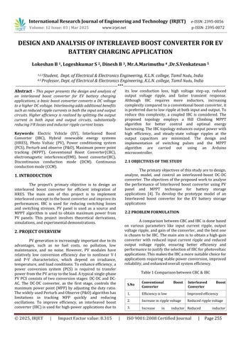
2.2 PROBLEM FORMULATION A comparison between CBC and IBC is done based on various parameters like input current ripple, output voltage ripple, and gain of the converter, and the best one is chosen to be IBC. The main aim is to obtain a high-gain converter with reduced input current ripple and reduced output voltage ripple, ensuring better efficiency and performance to justify the selection of IBC for photovoltaic applications .This makes the IBC a more suitable choice for applications requiring stable power conversion, improved reliability, and enhanced overall system efficiency.
2. PROJECT OVERVIEW PV generation is increasingly important due to its advantages, such as no fuel costs, no pollution, low maintenance, and no noise. However, PV modules have relatively low conversion efficiency due to nonlinear V-I and P-V characteristics, which depend on irradiance, temperature, and load conditions. To enhance efficiency, a power conversion system (PCS) is required to transfer power from the PV array to the load. A typical single-phase PV PCS consists of two conversion stages: DC-DC and DCAC. The DC-DC converter, as the first stage, controls the maximum power point (MPP) by adjusting the duty ratio. The widely used Perturb and Observe (P&O) algorithm has limitations in tracking MPP quickly and reducing oscillations. To improve efficiency, an interleaved boost converter (IBC) is used for high-power applications due to
© 2025, IRJET
|
Impact Factor value: 8.315
Table 1 Comparison between CBC & IBC
|
S.No
Conventional Converter
1.
Efficiency is low
Improved efficiency
2.
Increase in ripple voltage
Reduced ripple voltage
3.
Increase
in
Boost
Interleaved Converter
inductor Reduced
ISO 9001:2008 Certified Journal
|
Boost
inductor
Page 255