Mastering FPGA Chip Design
For Speed, Area, Power, and Reliability


Academy Pro Title by Kevin Hubbard


Academy Pro Title by Kevin Hubbard
Kevin Hubbard
● This is an Elektor Publication. Elektor is the media brand of Elektor International Media B.V.
PO Box 11, NL-6114-ZG Susteren, The Netherlands Phone: +31 46 4389444
● All rights reserved. No part of this book may be reproduced in any material form, including photocopying, or storing in any medium by electronic means and whether or not transiently or incidentally to some other use of this publication, without the written permission of the copyright holder except in accordance with the provisions of the Copyright Designs and Patents Act 1988 or under the terms of a licence issued by the Copyright Licencing Agency Ltd., 90 Tottenham Court Road, London, England W1P 9HE. Applications for the copyright holder’s permission to reproduce any part of the publication should be addressed to the publishers.
● Declaration
The authors and publisher have used their best efforts in ensuring the correctness of the information contained in this book. They do not assume, and hereby disclaim, any liability to any party for any loss or damage caused by errors or omissions in this book, whether such errors or omissions result from negligence, accident or any other cause.
● ISBN 978-3-89576-687-9 Print
ISBN 978-3-89576-686-2 eBook
● © Copyright 2024 Elektor International Media www.elektor.com
Layout: Kevin Hubbard
Printers: Ipskamp, Enschede, The Netherlands
Elektor is the world's leading source of essential technical information and electronics products for pro engineers, electronics designers, and the companies seeking to engage them. Each day, our international team develops and delivers high-quality content - via a variety of media channels (including magazines, video, digital media, and social media) in several languagesrelating to electronics design and DIY electronics. www.elektormagazine.com
1.1. What is Digital Logic Design?
2. History of the Computer Chip
2.1. First Integrated Circuits
2.2.
3.1. What is EDA?
3.3. EDA Definitions
3.4. Chapter Quiz
8.1. Hardware State Machines
8.2. Software State Machines
9.1. đSingle-Ended Signaling
9.2. đDifferential Signaling
9.3. đSERDES Transceivers
9.4. Optical Fiber
9.5. Chapter Quiz
10.1. Block
10.2. Using the RAMB36 in an Artix7 FPGA.
10.3. Block
FIFOs
11.1. Chapter Quiz
Clocking
12.1. Chapter Quiz
13. Timing Closure
16.2. Stimulus only
16.3. Test Vector Stimulus and Result Capture
16.4. Stimulus with
16.5. Chapter Quiz
17. Python Software
17.1. Software for Hardware Design
17.2. Hello World
17.3. Python Strings
17.4. đFile Filter
17.5. Cheats
17.6. Chapter Quiz
18. Digital Arithmetic
18.1. Unsigned Binary
18.2. Signed Magnitude
18.3. Two’s Complement
18.4. Fixed-Point
18.5. Floating-Point
18.6. đOverflow Detection and/or Saturation
18.7. đRounding
18.8. Pitfalls of working with two’s complement
19. Example Design - Blinky
19.1. Chapter Quiz
20.1. Pipelined Design
20.2. Simpler
21.1. Why đUART Serial Communications
21.2. đRS-232 .
21.3. Lesson-1 : Simple Loopback Design
21.4. Lesson-2 : UART RX Design
21.5. Lesson-3 : UART TX Design
21.6. Chapter Quiz
22. Design for Area
22.1. Even Free Gates Come at a High Price
22.2. Keep Track of Build Utilization Over Time
22.3. Use SRLs whenever possible
22.4. Minimize Saturation and Rounding Operations
22.5. Minimize RAM size
22.6. Minimize Register Widths
22.7. Minimize Bus Address Decoding
22.8. Shadow RAMs for Register Readback with Reset Clear Counters
22.9. Minimize Number of Clock Trees
23. Example Design - Mesa Bus
23.1. Mesa Bus Protocol
23.2. Local Bus over Mesa Bus
23.3. Building an FPGA with Mesa Bus
23.4. bd_server.py device driver to Mesa Bus
23.5. bd_shell.py Command Line Interface shell to Mesa Bus
23.6. mesa_bus_ex.py Example Python Client
23.7. Chapter Quiz
24. Design for Power
24.1. CV²F
24.2.
25.2. SUMPn-RLE Project History
25.3. SUMP3-RLE Features
25.4. SUMP3-RLE Example Hardware Design
25.5. SUMP3-RLE Software Tutorial
25.6. Chapter Quiz
26. Design for Reliability
26.1. Toss Bad Designs out the Window
26.2. Fixed Input / Output Timing
26.3. Clock Jitter
26.4. Power Rails
26.5. Adding Margin
26.6. Make Timing Closure
26.7. Resets
26.8. FSMs
26.9. Diagnostic Buses
26.10. Learn from Your Mistakes and Don’t Repeat Them
26.11. Register Packing
26.12. Thread Safety
26.13. Stuck Flops.
26.14. Clock Domain Crossing
26.16. Detect the Unexpected
26.17. Simulate the Unexpected
26.19. Faster than Fastest
26.20. Two’s Complement
26.21. Overflow Detection and Saturation, Interrupts
26.23. CRC32 Checking
26.24. Power-On Self-Test (POST)
27. Example Design - Video Graphics Controller
27.1. đCathode Ray Tube (CRT)
27.5. Video “Hello World” Test Pattern
27.6. Video Color Test Pattern
27.7. đVideo Frame Buffer
27.8. đVideo Text Buffer
27.9. đVideo Sprite Controller
27.10. Chapter Quiz
28. Design for Style
28.1. Long Hand Verilog
28.2. Net Naming Conventions
28.3. Source Code Width
28.4. Source Code Indentation
28.5. Avoid Magic Numbers
28.6. Comments
28.7. ASCII Art
28.8.
28.9.
Appendix A: Verilog vs VHDL
Appendix B: Write Your Own Book Using AsciiDoc
In the 1990s, digital logic designers experienced the rapid rise and fall of LSI Logic from Santa Clara, CA. It was a decade when suddenly everyone started designing custom digital ASICs instead of using discrete logic ICs on printed circuit boards. This new ASIC path required very little money and no chip foundry knowledge. LSI Logic knew how to do the “hard stuff” and sold this in exchange for a reasonable NRE and a small per chip margin. Silicon Valley experienced a surge of fabless semiconductor startups like NVIDIA, Broadcom, and Marvell Technology, as the industry embraced ASIC design.
LSI Logic’s business model revolved around providing Application-Specific Integrated Circuits (ASICs) to customers. They offered a fabless semiconductor model, meaning they designed and sold the chips but outsourced the manufacturing to external foundries. This approach allowed them to focus on design and innovation without the high costs associated with running their own fabrication facilities. Their business model was successful due to their ability to offer quick turnaround times and cost-effective solutions for custom chip design.
As Moore’s law progressed, a tectonic shift took place in the late 1990s as chip lithography entered the deep submicron era. At around 180 nm, chips became harder and more expensive to manufacture. ASICs became less affordable as reticle costs skyrocketed. Simultaneously, the industry transitioned from 8-inch (200mm) to 12-inch (300mm) wafers, essentially doubling the typical minimum order of custom chips within a single wafer boat processing of twenty-five wafers.
At the same time, FPGAs, a scrappy and costly technology from the 1980s, evolved from simple (and expensive) “glue logic” into cost-effective solutions for digital signal processing tasks that had previously been dominated by ASICs. ASIC vendors attempted to compete with the rapid rise of FPGAs by developing Structured ASICs but ultimately failed to keep pace with the rising costs associated with Moore’s Law-driven advancements, which favored the FPGA model of reticle expense amortization. While digital ASICs still exist, the number of yearly tape-outs continues to decline. The digital chip landscape had permanently changed.
In this evolving landscape, I’ve realized that the tools and design experience once required for large digital ASICs are now highly applicable to modern FPGA design—even more so as sub-nanometer FPGAs emerge on the horizon. Having worked in both industries for over thirty years, I find myself in the unique position of being able to share knowledge, bridging the worlds of ASIC and FPGA design.
Learning to write Verilog or VHDL that simulates is not particularly difficult. Writing RTL that simulates is only a small part of the chip designer’s job. The real challenge lies in designing a complete chip that is reliable and meets timing, area, and power budgets. This requires a much deeper understanding of the entire digital logic design process, all the way down to the CMOS transistor level.
This book is for Electrical Engineers wanting to learn those details and apply them towards designing large digital chips using modern FPGA technology.
Digital logic design is a field within electrical engineering and computer science that focuses on the design and implementation of digital circuits. These circuits use binary signals—0s and 1s—to perform a variety of tasks, ranging from simple logic operations to complex computations.
— Digital Logic Design
Digital logic designs do truly amazing things. They can implement complex state machines with latency of only a few nanoseconds. They can perform parallel digital signal processing at rates of multiple DVD movies per second. They can electrically interconnect simple semiconductor chips into an advanced circuit. Unlike CPUs, digital logic designs can do everything in parallel (all tasks at the same time) rather than sequentially (one task after the other).
MOSFET Transistor
The MOSFET (“metal-oxide-Semiconductor Field-effect transistor”) is the building block of modern digital chip designs. Its long history began with a patent filed by AustroHungarian born physicist Julius Edgar Lilienfeld in 1925 for a device that used an electric field to control current. William Shockley and others further developed the concept which eventually led to a working Junction Field-Effect Transistor (JFET) in the 1950s. In 1955, Lincoln Derrick and Carl Frosch grew a silicon dioxide layer over a silicon wafer and observed surface passivation effects. This discovery led to the MOSFET transistor being invented by Mohamed Atalla and Dawon Kahng at Bell Labs in 1959.
NOTE JFETs are still used in low-noise analog applications, while MOSFETs dominate the digital world.
By combining two types of MOSFET transistors (P and N), a CMOS gate is formed. MOSFETs rule the modern digital world as they are small, easy to manufacture, fast, and very low power. It is estimated that more than 20 trillion MOSFETs are manufactured every second.
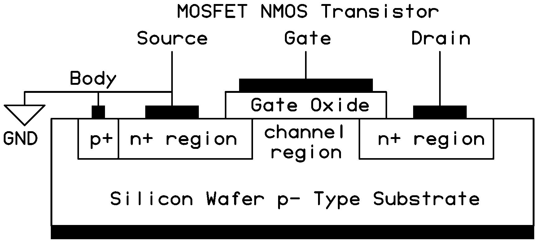
To create a MOSFET transistor, you start with a silicon wafer and dope regions to create two small n+ regions that surround the wafer’s default p- region. SiO2 (typically) is deposited above that NPN region to form a very thin gate oxide insulator. Connect some metal to the two n+ regions, the substrate body, and the gate oxide, and you have a MOSFET transistor. Modern MOSFETs primarily use a conductive polysilicon connector to the gate oxide. Maybe they should be called PSOSFETs instead!
Here’s the thing about silicon: Silicon is a chemical element (Si) on the periodic table. By itself, silicon is not a very good conductor. By adding (doping) a small amount of an element like phosphorus or boron—which are similar to silicon but have an extra or missing valence electron—things get really interesting. The doping process creates an imbalance in the number of electrons and holes within the crystal lattice structure, increasing conductivity. The result is a material that can function as either a strong insulator or a conductor—on demand.
I like to think of silicon like cookie dough: not very interesting by itself, but add some chocolate or butterscotch chips and BAM! You’ve made something really special.
Silicon Doping is the process of intentionally introducing impurities into pure silicon (or other semiconductors) to modify its electrical properties. This technique is fundamental in semiconductor manufacturing, enabling the creation of devices like diodes, transistors, and integrated circuits. In its natural state, silicon is a poor conductor because it has four valence electrons, forming a stable crystal structure with neighboring silicon atoms. Dopants are impurities added to silicon to increase its conductivity. Depending on the type of dopant used, the silicon can become either n-type or p-type.
Once the NPN-doped silicon structure is formed (as shown in the figure above), the ptype area directly beneath the gate creates the channel region, which may or may not permit electron flow.
The Channel of a MOSFET is the conductive path that forms between the source and drain terminals when the transistor is turned on. The channel is created when a voltage is applied to the gate, attracting charge carriers (electrons in N-channel MOSFETs, holes in P-channel MOSFETs) to form a conductive layer.
— Channel
Key Characteristics of a CMOS Gate:
• Insulated Control: The gate is separated from the channel by a thin layer of silicon dioxide (SiO2), creating a high-input impedance.
• Electric Field Activation: Applying a voltage to the gate generates an electric field, allowing current to flow between drain and source.
• Capacitive Behavior: The gate behaves like a capacitor.
An Electric Field is a region around an electrically charged object where other electric charges experience a force. This field represents the influence that a charge exerts on other charges in its vicinity, affecting them without direct contact.
Electrically, the gate of the NMOS transistor looks like a capacitor. Ignoring small amounts of leakage current, the transistor’s gate only requires energy when switching to charge and discharge its capacitance. When the gate is at GND potential, no current may flow through the NMOS transistor’s channel region. When a VCC voltage is applied to the gate, an electric field is created in the channel region and current may then flow between the drain and source.
NOTE
Analog designers often use VDD and VSS to represent the positive supply rail and ground nodes. In this book, I use VCC and GND—different names for the same thing, much like cilantro and coriander leaves. Transistorlevel designers may not appreciate this choice, but this is my book—and they’re more than welcome to write their own.
Power consumption of CMOS transistors is primarily dictated by CV²F, where:
• F is the gate switching frequency.
• C is the gate capacitance (including parasitic wiring).
• V² is the square of the voltage applied to the gate.
As Moore’s Law continues to shrink transistors, both V and C decrease, leading to lower power consumption and higher switching speeds.
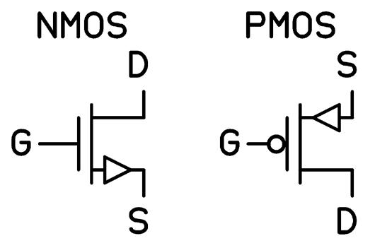
The “C” in “CMOS” stands for “Complementary”. MOSFETs come in complementary pairs called NMOS and PMOS. The NMOS transistor is built from the NPN structure described above, and is used to sink current on its Drain to a Source connected to GND. The PMOS transistor is the inverse. Built from a PNP structure, it is used to source VCC current from its Source node to its Drain node. The NMOS is turned “ON” by applying VCC to its Gate node. The PMOS is turned “ON” by applying GND to its Gate node.
NOTE
The terms PFET (P-channel Field-Effect Transistor) and NFET (N-channel Field-Effect Transistor) are also commonly used to refer to PMOS (Pchannel MOSFET) and NMOS (N-channel MOSFET) transistors.
When I think of MOSFET transistors, I like to think of three cookies in a row: chocolate chip, butterscotch chip, and chocolate chip. You turn the cookie channel on by dumping a bag of chocolate chips (excess electrons) next to the butterscotch chip cookie (at the Gate). Every butterscotch chip gets displaced by the chocolate chips from the bag, and now you have three chocolate chip cookies in a row (and the current flows). Anyone else hungry now?
TIP
It’s important to connect only digital signals to the digital input of a CMOS device. Connecting an analog signal to a digital input risks Simultaneous Conduction, a CMOS state where both NMOS and PMOS transistors conduct simultaneously, creating a resistive short circuit between VCC and GND. Picture a teeny-tiny Edison incandescent bulb inside your chip. This not only wastes power but also risks damaging the transistors due to overheating. Instead, use an analog comparator, and always follow the Vil and Vih specifications for a CMOS input to prevent this condition. Your tiny little CMOS transistors will thank you. Ignoring CMOS simultaneous conduction poses a serious risk to long-term system reliability.
For whatever reason, there is no universally agreed upon symbol set for NMOS and PMOS transistors. The figure above is just one of many that you may see in literature. For this reason, I will create my own to use in this chapter, as I think it conveys some important information. Also, this is my book—and no one can stop me.
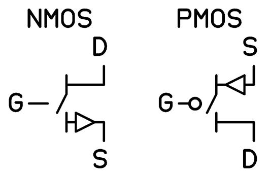
NMOS Symbol Information:
• Gate turns the channel on with a high(VCC) signal.
PMOS Symbol Information:
• Gate turns the channel on with a low(GND) signal.
The NMOS and PMOS can be thought of as Gate-controlled switches that have a small
amount of resistance in series with their switch. Drawing a CMOS inverter using modified NMOS and PMOS symbols illustrates the simplicity of building CMOS gates out of MOSFET transistors. This configuration is known as a CMOS totem-pole structure. The arrows in the MOSFET symbols do not represent diodes; rather, they indicate the direction of current flow when the channel is formed.
A CMOS Totem-Pole structure is a standard CMOS output configuration where a P-channel MOSFET is connected in series with an N-channel MOSFET, forming a push-pull circuit. The connection point between the two transistors serves as the output node.
— CMOS totem-pole

4. CMOS Inverter
The manufactured inverter would look like the following in a silicon wafer side-view.
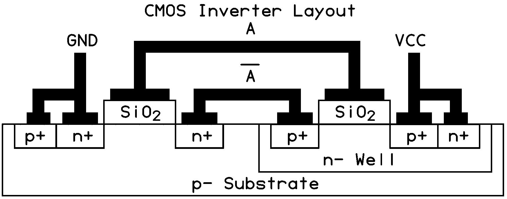
Figure 5. CMOS Inverter Layout
By adding just a few more NMOS and PMOS transistors in series and in parallel, more complicated gates like NANDs and NORs are easily created. Following them with another NMOS-PMOS pair (inverter) creates AND and OR gates.
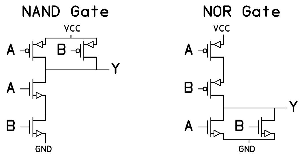
Figure 6. CMOS NAND and NOR Gates
For a deeper understanding of CMOS transistor fundamentals, I highly recommend “Principles of CMOS VLSI Design: A Systems Perspective” by Neil H.E. Weste and Kamran Eshraghian.
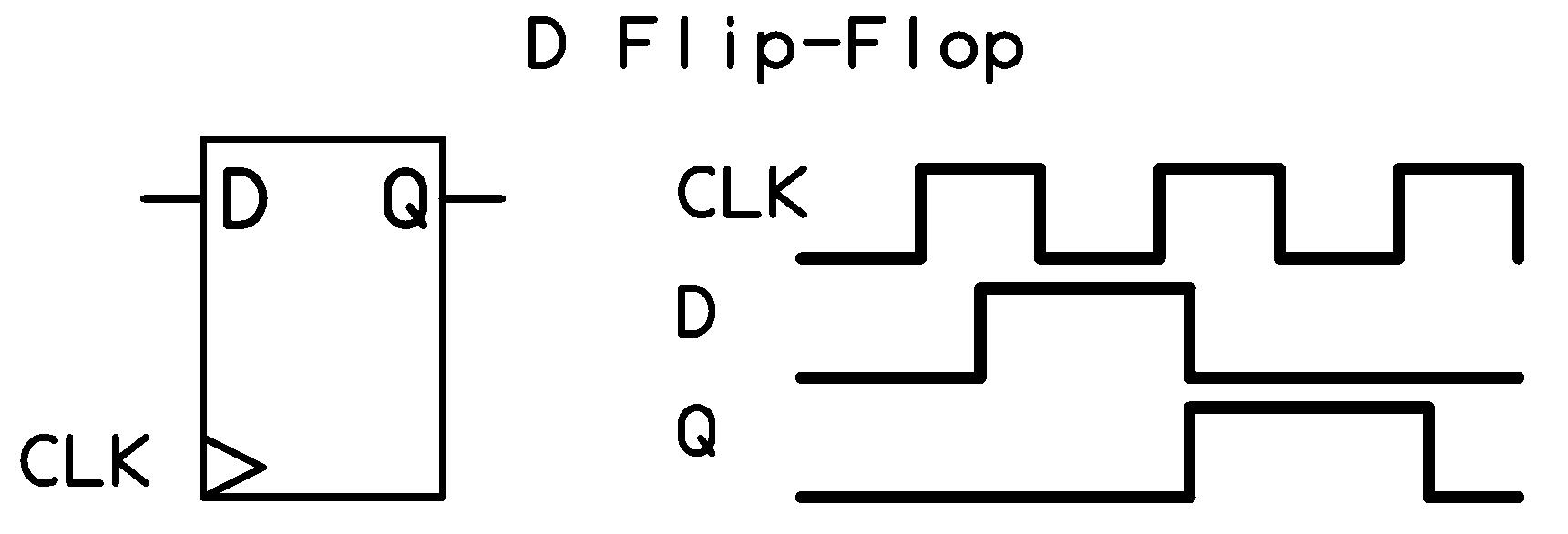
By combining digital logic gates like ANDs and ORs, more complex logic structures—such as adders, subtractors, comparators, and multipliers—can be created. However, these advanced structures alone have limited functionality, as they lack memory. They can compute an answer but cannot store it for another logic block to use. To achieve this, a digital storage element is required.
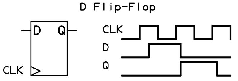
Figure 7. D-Type Flip-Flop
A D-type flip-flop (Data or Delay flip-flop) is a type of digital storage element used to store a single bit of data (0 or 1). It is one of the most commonly used types of flip-flops in digital circuits because it serves as a basic memory element that captures and stores the state of a signal. On the rising edge (or falling edge) of the clock signal (CLK), the value present at the D input is “latched” or captured and transferred to the output (Q). The output (Q) remains stable and does not change until the next clock edge, even if the D input changes between clock pulses.
— D-Type Flip-Flop
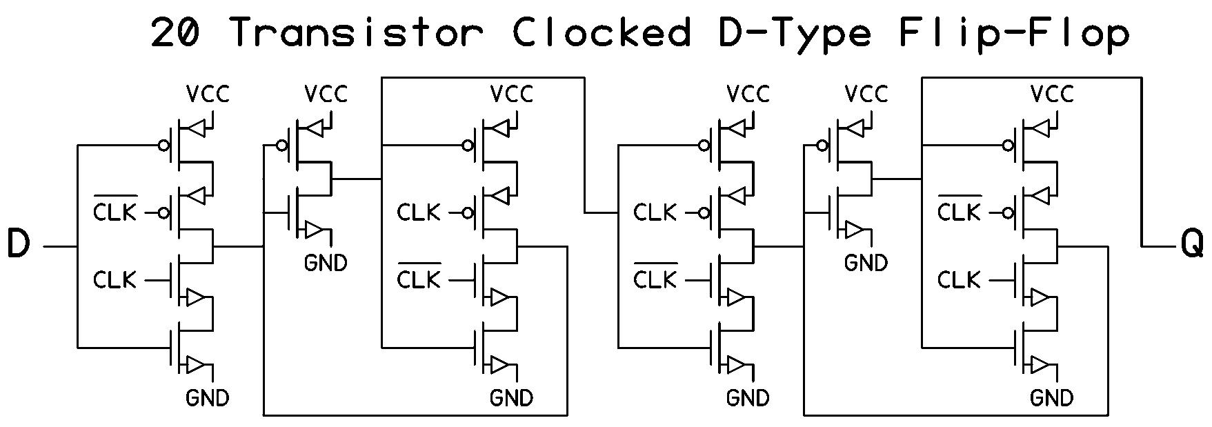
The D Flip-Flop is the primary building block of digital logic design. As a digital logic design deals with binary bits, the simple D Flip-Flop is the keeper of those bits. The smallest D Flip-Flop I have come across was made with twenty NMOS and PMOS transistors. You don’t need to know how it works, but you should know that those transistors are there. The eight transistors with clocks on their gates are especially important.
It’s extremely easy for an RTL designer to forget about the CMOS transistor structure of a D Flip-Flop. However, it’s important not to. It may also be tempting to assume that a flipflop with static input and output isn’t consuming much power. That assumption would be incorrect. The eight transistor gates driven by a clock represent eight capacitive loads, which, at CV²F, account for a significant portion of total power consumption in CMOS digital logic. In my experience, CMOS clock trees within a chip typically consume about one-third of the device’s total power.
To conserve power in a digital logic design, enable the clock to a flip-flop only when necessary. When the clock is gated, the Q output retains its logic state, and the flip-flop’s power consumption is reduced to nearly zero.
Pipelining, or adding flip-flops between combinatorial logic stages, is an important aspect of digital logic design for meeting timing. However, pipelining is not free, as it incurs a significant cost in both area and power. A good digital designer knows how to pipeline a design just enough to meet timing, but not so much that it needlessly consumes excessive area and power.
The Intel Pentium 4 is a classic example of over-pipelining a design. The 1990s saw 80x86 architecture rapidly go from 100 MHz to 1 GHz FMAX CPU designs. Intel’s performance desktop CPU plan for the 2000s was to then go from 1 GHz to 10 GHz. This plan resulted in the NetBurst microarchitecture, which more than doubled the traditional 80x86 pipelining. In the end, the Pentium 4 topped out at 3.8 GHz, and Intel abandoned NetBurst and backtracked to the much lower power Pentium M (Mobile) architecture initially intended only for laptops.
With CMOS clock frequencies reaching a ceiling of around 5 GHz, the industry’s focus has shifted to parallel processing, now fueling the rise of GPUs in AI. Meanwhile, FPGAs play a crucial role in parallel computing, offering significant growth potential for massively parallel signal processing.
QUESTION-1: MOSFET transistors? (Choose four)
☐ A) Come in Complementary PMOS and NMOS types.
☐ B) May be used as fast and small electrical switches.
☐ C) Are extremely rare and in short supply.
☐ D) Have many electrical characteristics resembling resistors and capacitors.
☐ E) Are manufactured at an astonishing rate.
Correct Answers: A, B, D, and E
QUESTION-2: Pipelining a digital design may result in? (Choose three)
☐ A) Faster clock frequencies.
☐ B) Faster simulation runtimes.
☐ C) Increased area.
☐ D) Increased power.
☐ E) Easier to read RTL.
Correct Answers: A, C, and D
QUESTION-3: CMOS Power may be reduced by? (Choose three)
☐ A) Decreasing Gate capacitance.
☐ B) Decreasing Gate toggling rates.
☐ C) Decreasing Gate voltage.
☐ D) Increasing channel length.
☐ E) Increasing transistor size.
Correct Answers: A, B, and C
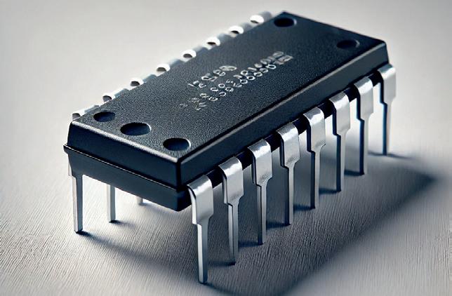
1959 was a pivotal year in electronics, as Robert Noyce at Fairchild Semiconductor and Jack Kilby at Texas Instruments simultaneously invented the first Integrated Circuit (IC). Unlike a single transistor, the integrated circuit housed multiple transistors on a single piece of semiconductor material. This breakthrough enabled the development of fully custom circuits, not on a circuit board, but on a single chip—revolutionizing modern electronics.
Integrated Circuit Key Features:
• Compact : Combines multiple electronic components into a small, efficient package.
• High Performance: Enables fast processing and low power consumption.
• Mass Production: Manufactured using photolithography, making ICs cost-effective.
In 1968, a group of engineers led by Albert Medwin at RCA developed the first commercially available CMOS integrated circuit—the RCA 4000 series (not to be confused with the Xilinx 4000 series of FPGAs). The 4000 series logic chips utilized CMOS transistor technology, which was much slower than the TTL-based 7400 series, but offered significantly lower power consumption. I got my start in electronics in the 1970s with these early 4000 series CMOS chips. A typical chip came in a 14- or 16-pin DIP package and contained four logic gates, such as AND, NAND, OR, and NOR.
A Dual In-line Package (DIP) is a standardized method for housing electronic components, especially integrated circuits (ICs). DIP packages consist of a rectangular housing with two parallel rows of pins extending perpendicularly from the sides of the IC. The number of pins can vary, but common counts are 8, 14, 16, or even higher. The pins are meant to fit through holes drilled in a printed circuit board (PCB) and are then soldered to create permanent connections.
— Dual In-line Package (DIP)
Early computers of the 1940s and 1950s were built using vacuum tubes. In the 1960s, digital computers transitioned to transistor-based designs and eventually to integrated circuits. During the 1960s and 1970s, non-CMOS transistors and integrated circuits dominated the field of digital electronics.
A Vacuum Tube, also known as a thermionic valve, is an electronic device that controls the flow of electric current within a vacuum-sealed glass or metal container. The tube contains a heated cathode, which emits electrons via thermionic emission, and an anode (plate) that attracts those electrons. A control grid is positioned between the cathode and anode, regulating electron flow to enable amplification or switching. The vacuum tube was a fundamental technology in early electronics, used for amplification, switching, and rectification before the advent of solid-state transistors.
— Vacuum Tube
In 1971, Intel introduced the 4004 CPU (not to be confused with RCA’s 4000 CMOS series of ICs). With only 2,300 transistors in a DIP16 package, it was revolutionary as the first CPU to be entirely contained within a single integrated circuit. Designed originally for calculators, the 4004 was succeeded by Intel’s 8008 (1972), 8080 (1974), and eventually the 8086/8088 (1979), which powered the original IBM XT computer.
Within just a few years of Intel’s 4004, Chuck Peddle and his team at MOS Technology designed the 8-bit 6502 CPU. Its exceptionally low cost was a game-changer, making advanced computing more accessible. The 6502 powered iconic systems such as the Apple II, Commodore 64, Atari 2600, and Nintendo Entertainment System, securing its place as one of the most influential processors in computing history.
Early personal computers, such as the IBM XT and Steve Wozniak’s Apple II, were built using dozens of discrete integrated circuits in small DIP packages, alongside an integrated CPU chip. The early 4000 series CMOS couldn’t reach 1 MHz clock speeds, so faster, higher-power TTL integrated circuits were used instead. It wasn’t until the early 1990s that CMOS technology became fast enough to replace TTL integrated circuits. Although ASICs were still a decade away, I consider the Intel 4004 CPU to be the first fully custom computer chip.
Application-Specific Integrated Circuit (ASIC) is a type of custom-designed chip optimized for a specific function rather than general-purpose computing. Unlike FPGAs (Field-Programmable Gate Arrays), which can be reprogrammed, ASICs are hardwired for a particular task, making them faster and more power-efficient for that application.
— Application-Specific Integrated Circuit (ASIC)
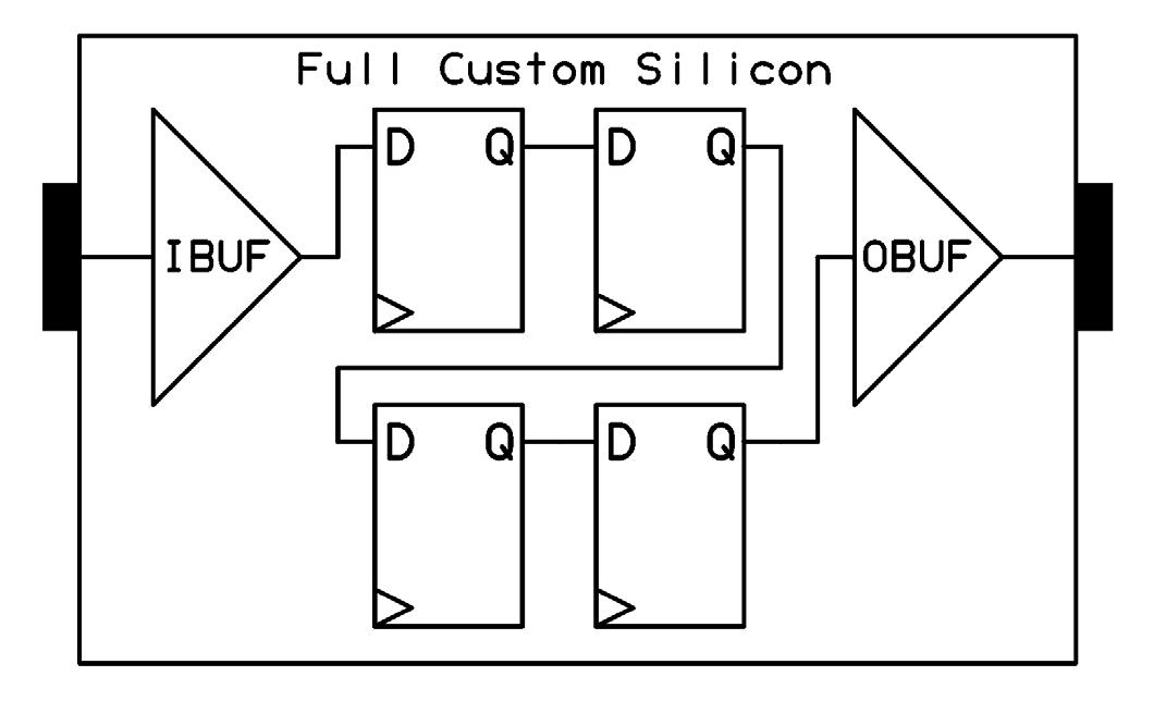
A full custom computer chip allows the designer to control every aspect of the design—from the size and placement of each transistor to the power rail locations and metal widths. For example, a fully custom silicon chip for a simple four-tap shift register could be designed using CMOS D flip-flops, optimizing compactness, speed, and power
efficiency. Ignoring power, ground, and clock, this device would have only two pins—an input and an output. The logic gates are positioned as close together as possible, and metal routing is kept short, ensuring no wasted silicon—resulting in a fully optimized design. Such a chip would be slightly smaller than a 4-bit 74HC93 counter. However, this small size and high speed come at a cost: Non-Recurring Engineering (NRE). NRE includes both the engineering effort (time and salary) and tooling expenses (reticles or masks) required to fabricate fully custom silicon. Paying the NRE delivers the smallest and cheapest silicon in high-volume production. But are there viable alternatives to high NRE costs?
Non-Recurring Engineering (NRE) refers to the one-time cost associated with the research, design, development, and testing of a new product or system. These costs are “non-recurring” because they are incurred only once during the initial development phase and do not repeat with the production of each unit.
— Non-Recurring Engineering (NRE)
Ignoring combinatorial logic for now, the simplest thing to build with a bunch of digital D Flops is a shift-register delay line. Below is an example implementation of a very simple four-tap shift-register design in full custom silicon.
Enter the Gate Array in the early 1980s. With Gate Arrays, a “generic” base wafer design is created that can potentially be used by multiple customers for completely different designs. The NRE for this base wafer can then be amortized down to very little. Think of Gate Arrays like a PCB fully stuffed with 7474 Flip-Flops and 7400-NAND ICs where, at the very end, a customer gets to add an additional two routing layers that are unique to their design, connecting all the chips. That’s a Gate Array.
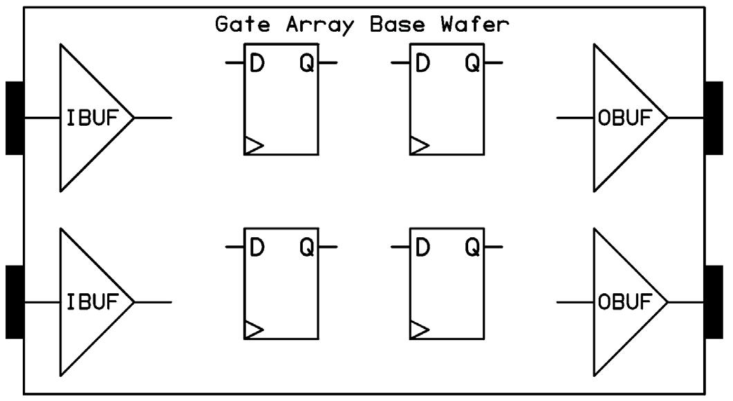
Starting with this base wafer, the end customer designs and pays for custom interconnect for this generic array of gates. Typically, this only requires custom reticles for one or two metal layers, making gate arrays very affordable. It can lower the price of entry to custom silicon design by 90%. Really. Gate-Arrays were that revolutionary in the 1980s and 1990s. I’ve done ASIC tape-outs that were the cost of my house and Gate-Array tape-outs that were the cost of my car. I definitely prefer the latter.
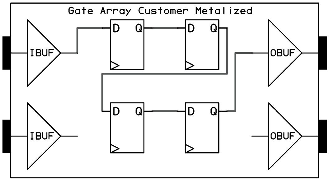
This lower Gate-Array NRE comes at a cost—the silicon size of the chip is significantly larger than a fully custom design. Why? The gates on the base wafer are deliberately spaced far apart to accommodate the varying routing demands of different customer designs. Achieving full gate utilization in a gate-array design is rare. For example, a vendor might offer base wafers with 10,000 or 20,000 gates. If your design requires 11,000 gates, you must use the larger 20,000-gate wafer. The same principle applies to package sizes and pin counts. So, while your NRE may be only 10% of a full custom design, your per-unit price could be 200% or 300% higher. In the end, even if NRE costs are nearly free, nothing is ever truly free.
Key Features of Gate Arrays:
• Semi-Custom Design: A predefined layout of transistors and logic gates.
• Customization via Metal Layers: The final circuit is defined by metal interconnects.
• Faster Development : Base silicon is pre-fabricated, ready for final metalization.
By the early 1990s, ASICs from LSI Logic Corporation had effectively wiped out the gatearray industry. ASICs provided most of the performance and cost advantages of full custom silicon, without the time and complexity of designing at the transistor level. Advances in EDA tools made ASIC design more accessible. Compared to gate arrays, ASICs offer higher performance, lower unit cost, and greater design flexibility, including memory integration and IP cores. While this decline was unfolding, a new technology—the Field Programmable Gate Array (FPGA)—entered the market.
In 1984, electrical engineer Ross Freeman conceived a brilliant and radical idea: a gate array that could be fully programmed in-field, rather than being permanently configured at the foundry using metal masks. This groundbreaking innovation led to the founding of Xilinx, which is now part of AMD.
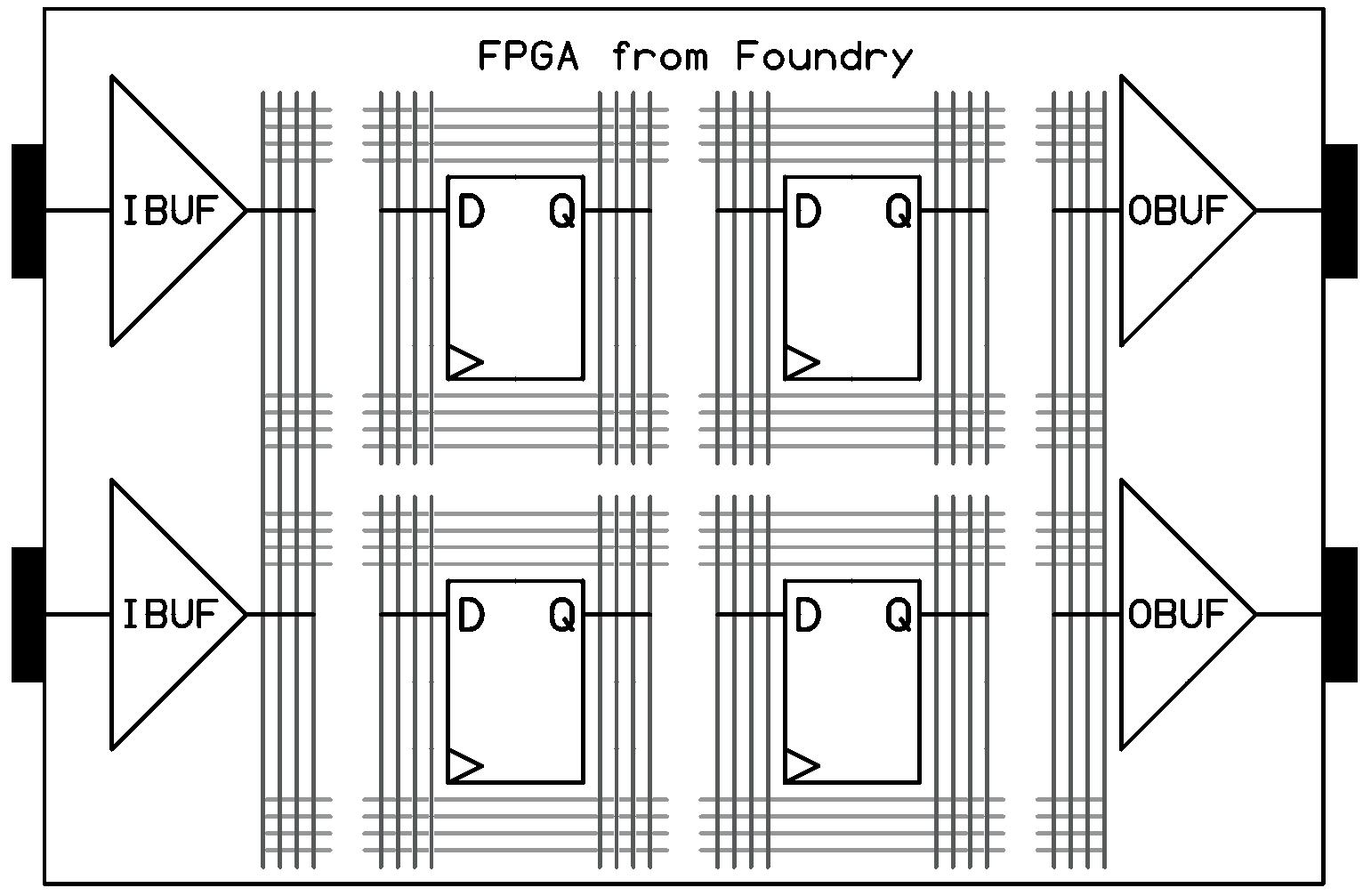
Just like a traditional gate array, an FPGA has a base-wafer-like design with gates that are initially unconnected and spaced far apart. However, unlike a gate array, an FPGA is fully metalized with a dense matrix of metal routing, enabling any flip-flop to connect to any other flip-flop across the chip. It’s somewhat analogous to a freeway system, where all onand off-ramps function as drawbridges that either open or close depending on the end user’s design.
These connections are established just after power-up using pass transistors, known as Programmable Interconnect Points (PIPs). It’s a fascinating concept—an off-chip EEPROM stores dozens of PIP configuration bits for each user-accessible flip-flop in the FPGA. Upon power-up, the EEPROM contents are loaded into a massive shift register of non-user flipflops, which then determine whether each PIP is opened or closed. This configuration process can take hundreds of milliseconds—an eternity in the digital realm.
A Programmable Interconnect Point (PIP) is a configurable switch within an FPGA’s routing architecture that allows signals to be dynamically connected between different logic elements.
Key Characteristics:
• Enables flexible routing between logic blocks.
• Controlled by configuration memory to establish connections.
• Uses pass transistors or antifuses depending on FPGA technology.
• Essential for FPGA programmability, allowing custom circuit designs.
— Programmable Interconnect Point (PIP)
At the bitstream level, designing an FPGA is similar to designing a printed circuit board—the designer determines how components connect electrically, but within the chip itself. Fortunately, with millions to billions of PIPs to configure, modern EDA tools provide higher levels of abstraction, such as Register Transfer Level (RTL), to streamline the process.
My super-simple FPGA example below has only four user flip-flops but more than 400 PIPs. These PIPs are not drawn to scale—in reality, they are much larger than a single metal via in silicon.
The AMD/Xilinx Artix-7 XC7A35T FPGA, featured later in this book, has 40,000 flip-flops and requires 1,600,000 PIP configuration bits. Fortunately, flash memory is now incredibly cheap—a stark contrast to its cost in the 1980s and 1990s. A $100 FPGA might have an external flash EEPROM priced at just $1 or $2.
Ross Freeman’s brilliance wasn’t just about skating to the puck—it was about skating to where the puck was going. I can’t help but wonder if he might have been Canadian.
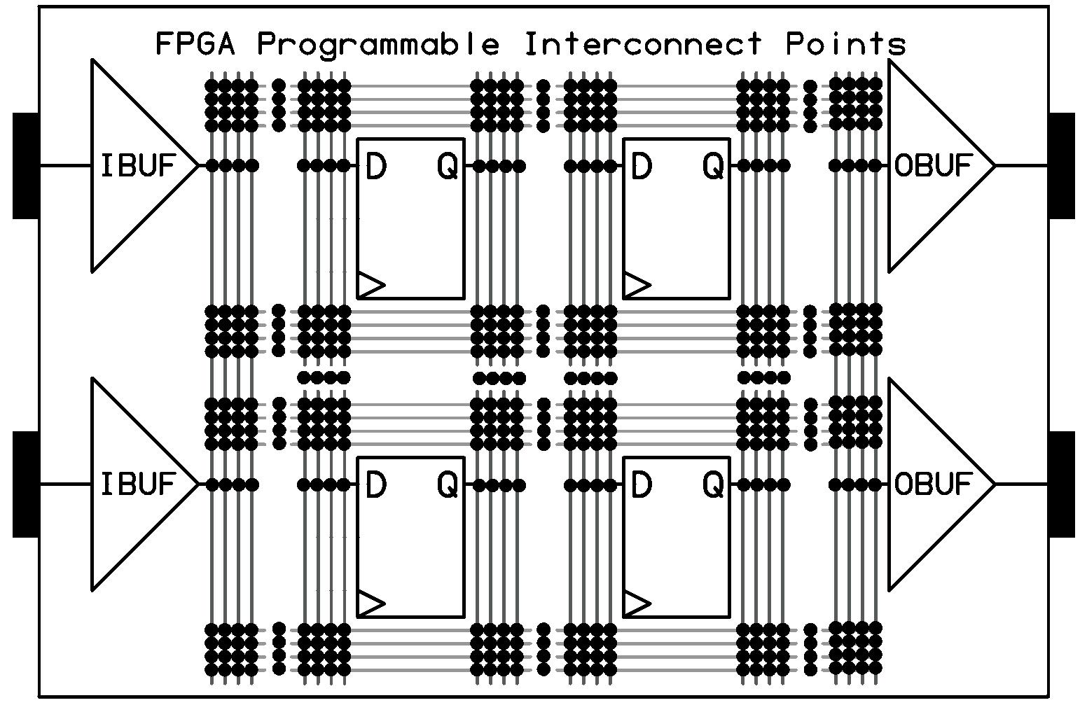
Excluding diffused IP like multipliers and RAMs, the actual overhead for an FPGA compared to custom silicon is approximately 10×. In other words, a purely digital logic design will consume about 10× the CMOS area in an FPGA compared to an ASIC. FPGAs are larger and more expensive than custom silicon, but with non-recurring engineering (NRE) costs for custom silicon now exceeding $1 million USD, they remain viable for lowvolume designs. Would a company be better off spending $1M in NRE for a $10 ASIC, or opting for $0 NRE and $100 per FPGA? Ay, there’s the rub.
Diffused IP refers to intellectual property (IP) that is physically embedded into a semiconductor device during the manufacturing process. Unlike soft IP, which is implemented using HDL code, or firm IP, which is partially synthesized, diffused IP is hardwired into the silicon at the mask level.
The original 4-tap shift register design implemented in the above FPGA would look like this:
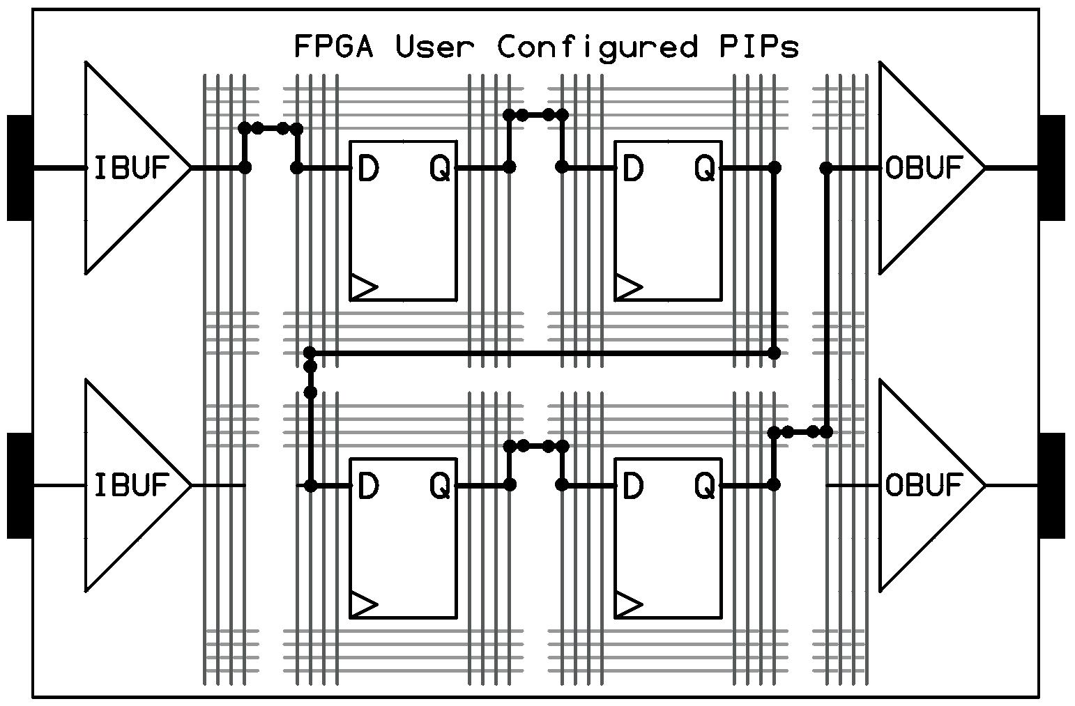
Figure 14. Four-Tap Shift-Register implemented in FPGA technology
What’s noteworthy is that the vast majority of metal routing channels in an FPGA go unused—only a small fraction of Programmable Interconnect Points (PIPs) are actually closed. Even open PIPs consume die area and must be accounted for in both wafer test time and silicon area.
Routing in an FPGA is also significantly slower than in full custom silicon. Not only are the routes much longer (the die may be ~10× larger, increasing capacitance), but each PIP introduces parasitic resistance and capacitance, unlike the near-zero parasitics of metal vias in fully custom ASIC, ASSP, or Gate-Array designs. These PIP-connected Manhattan routes take nanoseconds instead of hundreds of picoseconds to propagate signals.
Early 350 nm FPGAs were slow, operating at only 20–40 MHz. Today’s 28 nm and 16 nm FPGAs achieve 200–300 MHz for many designs. My rule of thumb is that FPGA fabric is roughly ten times slower than an ASIC made using the same CMOS generation.
So, what does this all mean? FPGAs will never compete with full custom silicon for highperformance computing, such as 3 GHz CPUs and GPUs. However, for many applications, 300 MHz is “good enough”, and million-dollar NREs make ASIC development prohibitively expensive for lower-volume designs.
Full Custom, Standard Cell ASICs, Gate Arrays, and FPGAs represent the full spectrum of semiconductor digital chip design. The key difference lies in how much of the physical implementation is handled by the digital logic designer versus the semiconductor vendor. By raising the abstraction level to LUTs and flip-flops, a single digital designer can now rapidly implement a one-billion-transistor chip using FPGA technology.
QUESTION-1: FPGAs are inherently slower than ASICs because? (Choose three)
☐ A) ASIC gates are faster than FPGA gates.
☐ B) FPGA gates are located further apart than ASIC gates.
☐ C) FPGA routing involves resistive PIPs.
☐ D) FPGA routing may take long indirect routes with high capacitance.
☐ E) ASIC NRE is much higher than FPGA NRE.
Correct Answers: B, C, and D
QUESTION-2: FPGA Programmable Interconnect Points (PIPs)? (Choose five)
☐ A) Provide FPGAs with configurable routing.
☐ B) Create additional routing resistance.
☐ C) Create additional routing capacitance.
☐ D) Contribute to FPGAs being approximately 10× slower than ASICs.
☐ E) Are mostly unused, offering configurability at the cost of area.
Correct Answers: A, B, C, D, and E
QUESTION-3: Gate Arrays? (Choose two)
☐ A) Provide near ASIC performance at much lower NRE.
☐ B) Can be field-programmed, unlike an FPGA.
☐ C) Are customized through metal layers.
☐ D) Allow customers to size transistors for power, area, and speed.
☐ E) Are a rapidly growing technology, overtaking FPGAs.
Correct Answers: A and C
Albert Medwin, 11
Alpha Transparency Key, 311
Application-Specific Integrated Circuit (ASIC), 12
Aspect Ratio, 89
Automatic Test Pattern Generation (ATPG), 23
B
bd_shell, 269
Bell Labs, 3
Bijan Davari, 70
Bit Growth, 185
Bit-Bucket, 234
Built In Self Test (BIST), 23
C
Carl Frosch, 3
Cathode Ray Tube, 287 Channel, 4
Chiplet, 130
ChipVault, 47
Chuck Peddle, 12
Clock and Data Recovery (CDR), 117
Clock Domain Crossing, 95
Clock Tree Insertion Delay, 116
Clock Tree Synthesis (CTS), 23
CMOS Totem-Pole, 7
Coding Style, 315
Command Line Interface (CLI), 139
Corner Conditions, 116
Current Mode Logic, 80
CV²F, 5
Cyclic Redundancy Check 32 (CRC32), 285
D
D Flip-Flop, 9
Dawon Kahng, 3
Defect Density, 128
Design Hierarchy, 47
Design Rule Checking (DRC), 24
Device Under Test (DUT), 153
Differential Signaling, 73
Diffused IP, 17
Digital Arithmetic, 179
Digital Signal Processing (DSP), 189
Doping, 4
E
EDIF, 28
Electric Field, 5
Electromigration Breakdown, 24
Electronic Design Automation (EDA), 19
Electrostatic Discharge (ESD), 31
FFairchild Semiconductor, 11
Field Application Engineer (FAE), 21
Field Programmable Gate Array (FPGA), 15
FIFO, 95
File Filter, 171, 171
Finite State Machine (FSM), 59
Five-by-Five, 235
Fixed-Point, 182
Floating-Point, 184 Floorplanning, 128
Frequency Synthesis, 107 Full Custom, 12
G
Gate Array, 13 Git, 56 Grep, 167
H
Hardware Description Language (HDL), 28 Hello, World!, 191
IILA, 243
Infer, 35
Integrated Circuit (IC), 11
Interpreted Language, 168 Inverter, 7
J
Jack Kilby, 11
John Ousterhout, 33
John von Neumann, 181
Julius Edgar Lilienfeld, 3
Junction Field-Effect Transistor (JFET), 3
Karnaugh Map Optimization, 41
Known Good Die (KGD), 23
L
Lincoln Derrick, 3
Linear-Feedback Shift Register (LFSR), 285
Linus Torvalds, 142 Linux, 142
Load Capacitance, 239 Local Bus, 230
Look-Up Table (LUT), 41 Low Voltage CMOS, 72 LSB, 180 LVDS, 73
M
Manhattan Routing, 45 Mapper, 24
Mesa Bus Protocol, 229 MicroBlaze™, 66 Module, 47
Mohamed Atalla, 3 MOSFET, 3 MSB, 180
N
NAND, 7
Non-Recurring Engineering (NRE), 13 NOR, 7
O
One-Hot, 61
Open-Drain Output, 78
Overflow Detection and/or Saturation, 185
P
Pad Limited Design, 220
Parasitic Wiring Delay, 125 PEP 8, 171
Phase-Locked Loop (PLL), 104 Placement, 126
Placer, 24
Power Solution, 24
Power-On Self-Test (POST), 285
Process, Voltage, and Temperature (PVT), 116
Programmable Interconnect Point (PIP), 15 Python, 168
Raster Display, 288
RC Extraction, 24
RCA, 69
Refactoring, 319
Regional Clock Gating, 240
Register Retiming, 123
Register-Transfer Level (RTL) Simulator, 136
Register-transfer-level (RTL), 35 RLC Delay, 132
Robert Noyce, 11
Ross Freeman, 15
Rounding, 186 RS-232, 206
Run-Length Encoding (RLE), 243
S
Scientific Notation, 184
SERDES Transceivers, 79
Setup and Hold Times, 112
Shift Register LUT (SRL), 220
Signed Magnitude, 180 Silicon, 4
Simultaneous Conduction, 6
Simultaneously Switching Outputs (SSO), 78
Single-Ended Signaling, 71
Standard Delay Format (SDF), 24
Static Timing Analysis, 24
Steve Wozniak, 12
Structural Level Abstraction, 27 SUMP3, 243
Synthesis, 22
SystemVerilog, 165
T
Tape-Out, 25
Test Bench, 153
Test Insertion, 23
Test Vector, 160
Texas Instruments, 11
Thread Safety, 279
TI Fixed-Point Notation, 183
Timing Arcs, 120
Timing Closure, 111
Timing Skew, 103
Two’s Complement, 181
U
UART, 205
Unsigned Binary, 179
User Bus, 270 V
Vacuum Tube, 12
Value Change Dump (VCD), 142
Video Frame Buffer, 299
Video Graphics Array, 289
Video Graphics Controller (VGC), 287
Video Sprite Controller, 307
Video Text Buffer, 302
Wafer Testing, 23
Watchdog Timer (WDT), 66
This book teaches the fundamentals of FPGA operation, covering basic CMOS transistor theory to designing digital FPGA chips using LUTs, flip-flops, and embedded memories. Ideal for electrical engineers aiming to design large digital chips using FPGA technology.
Discover:
> The inner workings of FPGA architecture and functionality.
> Hardware Description Languages (HDL) like Verilog and VHDL.
> The EDA tool flow for converting HDL source into a functional FPGA chip design.
> Insider tips for reliable, low power, and high performance FPGA designs.
Example designs include:
> Computer-to-FPGA UART serial communication.
> An open-source Sump3 logic analyzer implementation.
> A fully functional graphics controller.
What you need:
> Digilent BASYS3 or similar FPGA eval board with an AMD/Xilinx FPGA.
> Vivado EDA tool suite (available for download from AMD website free of charge).
> Project source files available from author’s GitHub site github.com/blackmesalabs.

Kevin Hubbard holds a BSc in Electrical Engineering from the University of Washington. His passion for digital electronics began in the late 1970s designing logic circuits for his 8-bit home computers. Over his 30+ year career, Kevin has specialized in digital ASIC and FPGA design in the Wireless Data and Medical Devices industries. In 2013, he founded Black Mesa Labs to develop and promote open-source software and hardware. He can be reached on X at @bml_khubbard.
Elektor International Media www.elektor.com