MicrowaveWireless Communications FromTransistorto SystemLevel
UniversityofFerrara,Ferrara,Italy
UniversityofMessina,Messina,Italy
AntonioRaffo
GiovanniCrupi
AMSTERDAM • BOSTON • HEIDELBERG • LONDON NEW YORK • OXFORD • PARIS • SAN DIEGO SAN FRANCISCO • SINGAPORE • SYDNEY • TOKYO Academic Press is an imprint of Elsevier
AcademicPressisanimprintofElsevier
32JamestownRoad,LondonNW17BY,UK
525BStreet,Suite1800,SanDiego,CA92101-4495,USA
50HampshireStreet,5thFloor,Cambridge,MA02139,USA
TheBoulevard,LangfordLane,Kidlington,OxfordOX51GB,UK
Copyright # 2016ElsevierLtd.Allrightsreserved.
Nopartofthispublicationmaybereproducedortransmittedinanyformorbyanymeans, electronicormechanical,includingphotocopying,recording,oranyinformationstorage andretrievalsystem,withoutpermissioninwritingfromthepublisher.Detailsonhowto seekpermission,furtherinformationaboutthePublisher’spermissionspoliciesandour arrangementswithorganizationssuchastheCopyrightClearanceCenterandthe CopyrightLicensingAgency,canbefoundatourwebsite: www.elsevier.com/permissions.
Thisbookandtheindividualcontributionscontainedinitareprotectedundercopyright bythePublisher(otherthanasmaybenotedherein).
Notices
Knowledgeandbestpracticeinthisfieldareconstantlychanging.Asnewresearchand experiencebroadenourunderstanding,changesinresearchmethods,professional practices,ormedicaltreatmentmaybecomenecessary.
Practitionersandresearchersmustalwaysrelyontheirownexperienceandknowledge inevaluatingandusinganyinformation,methods,compounds,orexperimentsdescribed herein.Inusingsuchinformationormethodstheyshouldbemindfuloftheirownsafetyand thesafetyofothers,includingpartiesforwhomtheyhaveaprofessionalresponsibility.
Tothefullestextentofthelaw,neitherthePublishernortheauthors,contributors,oreditors, assumeanyliabilityforanyinjuryand/ordamagetopersonsorpropertyasamatterofproducts liability,negligenceorotherwise,orfromanyuseoroperationofanymethods,products, instructions,orideascontainedinthematerialherein.
BritishLibraryCataloguinginPublicationData
AcataloguerecordforthisbookisavailablefromtheBritishLibrary LibraryofCongressCataloging-in-PublicationData
AcatalogrecordforthisbookisavailablefromtheLibraryofCongress
ISBN:978-0-12-803894-9
ForinformationonallAcademicPresspublications visitourwebsiteat http://store.elsevier.com/
Publisher: JoeHayton
AcquisitionEditor: TimPitts
EditorialProjectManager: CharlieKent
ProductionProjectManager: JasonMitchell
Designer: VictoriaPearson
PrintedintheUnitedStates
AdAlessandro,l’Amoredipapà AntonioRaffo
AimieicarigenitoriCarmeloeTeresa AimieifratelliVincenzo,Felice,IsodianaeGiuseppe EdamiamoglieGabriella
GiovanniCrupi
Contributors
G.Avolio
KULeuven,Leuven,Belgium
K.Burger
Qualcomm,SanDiego,CA,UnitedStates
A.Caddemi
UniversityofMessina,Messina,Italy
V.Camarchia
PolitecnicodiTorino,Torino,Italy
W.Chen
TsinghuaUniversity,Beijing,China
X.Chen
TsinghuaUniversity,Beijing,China
E.Cipriani
UniversityofRomeTorVergata,Rome,Italy
P.Colantonio
UniversityofRomeTorVergata,Rome,Italy
G.Crupi
UniversityofMessina,Messina,Italy
S.Farsi
KULeuven,Leuven,Belgium;QualcommInc.,SanDiego,CA,UnitedStates
A.Ferrero
KeysightTechnologies,SantaRosa,CA,UnitedStates
F.Giannini
UniversityofRomeTorVergata,Rome,Italy
E.McCune
RFCommunicationsConsulting,SantaClara,CA,UnitedStates
B.Moser
Qorvo,Inc,Greensboro,NC,UnitedStates
M.Pirola
PolitecnicodiTorino,Torino,Italy
A.Raffo
UniversityofFerrara,Ferrara,Italy
F.Ramirez
UniversityofCantabria,Santander,Spain
xiii
S.Sancho
UniversityofCantabria,Santander,Spain
D.M.M.-P.Schreurs
KULeuven,Leuven,Belgium
A.Suarez
UniversityofCantabria,Santander,Spain
G.Vannini
UniversityofFerrara,Ferrara,Italy
Z.Wang
MicrosoftCorp.,Beijing,China
P.J.Zampardi
Qorvo,Inc,NewburyPark,CA,UnitedStates
S.Zhang
SmarterMicroInc.,Shanghai,China
xiv Contributors
ForewordbyRameshK.Gupta
Systemsengineeringenablestherealizationofcomplexsystemfunctionsthrough carefulchoice,andacombinationofinteractingsystemelementsassembledto achievespecificanddefinedobjectives.RFandmicrowavesystemsaredesigned forapplicationssuchasradioastronomyandspaceexploration,navigation,radars, wirelessterrestrialandsatellitecommunications,remotesensing,RFidentification, electronicwarfare,medicalimaging,monitoringandsensing,automotivecollision avoidancesystems,etc.Typically,theseRFsystemsareintegratedwithvarioussubsystemsandelements,suchaslow-noiseamplifiersandfrontends,frequency sources,frequencyconverters,intermediateandhighpoweramplifierswithtransmit and/orreceiveantennas,andradiatingelements.RealizationoftheseRFsubsystems oftenrequireshighfrequencyRFtransistorsanddevicesthatareembeddedand assembledwithpassivecircuitsofmicrostriplinesprintedonasubstrate,and/or coaxialorwaveguideelements,usedinthedesignandparticularwirelesscommunicationapplication.
EffectiveRFandmicrowavesystemsengineeringrequiresanin-depthunderstandingofinteractionsbetweendevices,circuits,andsystemsfordeveloping solutionsthatcanbemanufacturedcost-effectively,andwithrequiredperformance, repeatability,andreliability.Thisisparticularlyimportantforhighvolumedeploymentandproductionofwirelesssystemsanduserequipment,includinghand-held andwearabledevices(eg,smartphones,tablets,smartwatches,etc.)whereconsumersdemandthehighestperformance,functionality,andrepeatableperformance atthelowestpossibleprice.Ithasbeenachallengeforpracticingwirelesscircuit, devicedesign,andsystemengineerstofindtherequisiteinformationfortheirdesign anddevelopmentefforts.Therefore,IbelievethatDr.AntonioRaffoandDr.GiovanniCrupi,theeditorsofthebook“MicrowaveWirelessCommunications:From TransistortoSystemLevel ,”havedoneagreatservicetothemicrowaveandRFcommunitybyputtingtogetherimportantandrelevantinformationonsystems,circuits, anddevicesinasinglevolumewithcontributionsfromauthorsthathaveextensive researchexperienceandexpertiseinthespecifictechnicalareasandtopicsincluded ineachoftheeightchapters.
Goingthroughthetableofcontentsforthisbooksentmeonanostalgicjourney throughmyowncareer,whichspannedworkinRFdeviceandcircuitmodeling, satelliteandwirelesssubsystemdevelopmentandsystemdesign,andmodeling, aswellasthedeploymentandoperationsofthesesystemsanddevices.Istarted mycareerwiththeinvestigationoftwo-terminalsolid-statedevices,suchasGunn andIMPATTdiodes,forsystemapplications.TheissuesofRFparameterdeembedding,linearandnonlinearcircuitanalysisandmodeling,aswellastheirnoise behavior,wererelevantthenfortheirsysteminsertion.Thetwo-terminalRFdevices werequiteconstrainedbecauseoftheir“noisybehavior”andsignaldistortioncharacteristicsduringlargesignalconditions.Emergenceofthree-terminalGallium Arsenidemetal-semiconductorfield-effecttransistors(MESFETs)andthemany
xix
derivatives—includinghighelectronmobilitytransistors(HEMTs)andpseudomorphicHEMTs(p-HEMTs),etc.—andtheirintegrationontomonolithicmicrowave integratedcircuits(MMICs)onGaAssubstrates,aswellasdevelopmentofsilicon basedRFintegratedcircuits(RFICs),havehadarevolutionaryimpactontheminiaturizationofRFsystems.SomeexamplesofthesesystemsincludethehighperformanceradarsusingT/Rmodules,satellitesystemswithflexibleandsteerablebeams, andwirelesssystemswithsmallersize,broaderbandwidth,andrepeatableperformancewithhigherreliability.Byeffectivesystemdesign,thesesystemscanbemanufacturedanddeployedatasignificantlyreducedcost.DuringmyworkatCOMSAT Laboratories,usingthedevice,circuit,system,measurement,andcalibrationtechniquessimilartoonesdocumentedinallthechaptersofthisbook,wewereable todevelopminiaturizedreceivers,poweramplifiersandtransmitters,frequencyconverters,andswitchmatricesfordynamicsatellitebeamswitching.Wealsosuccessfullydevelopedproof-of-conceptC-,X-,andKu-bandphasedarrayantennasfor satellitebeamshapingandsteeringforon-boardandgroundsatelliteapplications. Itisgratifyingtoseemanyofthesesubsystemsandsystemsandtheirderivatives nowbeingcomponentsofthemajorityofmodernsatelliteandwirelessnetwork architectures.
GiventhestateoftheRFandmicrowavetechnologytoday,Iremainveryenthusiasticonemergenceofnewinnovativewirelesssystems.Duringthecomingyears anddecades,manynewapplicationsarelikelytobecomeavailable,includingwearablehealthcaredatasensingandmonitoringsystems,self-energizingimplantable medicalsystems,autonomousandinterconnectedvehicles,collisionavoidancesystems,nondestructivemedicalimagingusingterahertz(THz)frequencies,contactless paymentsystems,etc.Itismyhopethatstudents,engineers,andresearchers involvedinRFandmicrowavepracticewillbeabletoenhancetheirunderstanding ofdevice,circuit,andsysteminteractionsthroughconceptsandtechniquespresented inthisbook,andhelpcreateexcitingsystemapplicationsandsolutionsforthebenefit ofmankind.
Bethesda,Maryland,UnitedStates xx ForewordbyRameshK.Gupta
RameshK.Gupta,Ph.D.
Preface
Thewirelesscommunicationmarkethaswitnessedtremendousgrowthinrecent years.Totheconsumer,thisgrowthmanifestsitselfviatheproliferationofmobile telephones,tablets,gamingconsoles,andsoon,theInternetofThings.Thedesignof thesewirelesscommunicationsystemsrequiresin-depthunderstandingoftheir microwavefunctionality,startingfromthetheoreticalunderpinningsoftheirinner workingstotheirpracticalsystem-leveldeployment.
Thedesignofmicrowavewirelesssystemstraversesthreedifferentstages,oftentimesdubbedthedevice,circuit,andsystemlevels.Inspiteofthevastarchivalliteraturedealingwitheachofthesedesignlevels,thusfarnobookhasdetailedthe linksandinteractionsamongthem.Notsurprisingly,microwaveengineersoften acquiredeepexpertiseinonelevel,butlackunderstandingofotherlevels,especially theirinteractions,whichcomplicatesthecollaborationandprojecthandoverbetween designteams,andstiflesinnovation.Asanexample,engineersworkingondevice modelingoftentimesexperiencedifficultiesunderstandingthedifferentoperating modesoftransmittersbasedondynamicpowersupplypoweramplifiers(DPSPA),despitethefactthatDPS-PAoperatingmodesareinherentlyandsimplyrelated totransistoroperation.
Thegoalofthisbookistoelucidatelinksbetweenthedifferentlevelsinmicrowavewirelesssystemdesignbydescribingandunravelingtheirinteractions.The book’smultipleexpertauthorsofferdistinctandcomplementaryviewpointsof thesubjectmaterial.Together,theirtwoforewordsandeightchaptersprovidecomprehensivecoverageofthevasttopicarea.Whileindividualcontributionsfocusprimarilyononeofthethreedifferentdesignlevels,altogethertheyalsotouchon interactionsbetweenlevels,andaddressthepresentlysiloedknowledgeofthesubjectfield.Forexample,thereaderwilllearnthatdesignlinksbetweenthedevice andthecircuitlevelsarenotsodifferentwhendealingwithamplifiers,mixers,or oscillators,andthatlimitationsarisingfromtransistorlinearandnonlinearparasitic elementsarelargelythesame,eventhoughtheyimpactdifferentquantities(noise, poweraddedefficiency,conversiongain,resonanceconditions).
Wehopethisbookwillbecomeavaluedresource,notonlyforresearchers,engineers,andteacherswishingtoextendtheirknowledgeofmicrowavewireless systemsbeyondthepresentlystratifiedliterature,buttoallthoseseekingabetter understandingofthelinkagesanddependenciesbetweendifferentdesignlevels.
Weverymuchhopethatthereaderwillenjoyherorhisjourneythroughthethree differentlevelsofthemicrowavewirelesssystemdesign!
xxi
AntonioRaffoandGiovanniCrupi
Microwavetransistor modeling 1
G.Crupi*,A.Raffo†,G.Avolio{,A.Caddemi*,D.M.M.-P.Schreurs{ andG.Vannini†
UniversityofMessina,Messina,Italy* UniversityofFerrara,Ferrara,Italy† KULeuven,Leuven,Belgium{
CHAPTEROUTLINE
1.1 INTRODUCTION
Microwavetransistormodelingisanevergreenresearchfieldofparamountimportance.Thesignificantinterestaroundthistopiccomesfromthefactthatthetransistor isthekeycomponentinhigh-frequencycircuitsthatareattheheartofmodernwirelesscommunicationsystems,suchasmobiletelephony.Tomeetthemoreandmore stringentrequirementsofwirelesscommunicationsystems,transistortechnologies areincessantlyprogressing.Hence,theneedforexploitingemergingtechnologies attheirbestmakesmicrowavetransistormodelinganopenresearchfieldincontinuousevolution.
Thisfirstchapterismeanttogiveacomprehensiveoverviewofthefundamentals, state-of-the-art,challenges,andfuturetrendsinthefieldofmicrowavetransistor modeling,goingfromlinear(alsonoise)tononlinearoperation.
Thechapterisstructuredintosixmainsections,includingthisintroduction.The nextsectionisdevotedtothemicrowavetransistortechnologies.Ofthevarious microwavetransistors,theanalysisofthepresentchapterisfocusedonthehighelectron-mobilitytransistor(HEMT).Hence,thephysicalstructureandtheoperation principlesofthismicrowaveactivesolidstatedeviceareconciselyreviewed.
CHAPTER
1.1Introduction........................................................................................................ 1 1.2MicrowaveTransistorTechnologies..................................................................... 2 1.3TransistorModeling............................................................................................ 7 1.4Small-SignalModeling........................................................................................ 9 1.5NoiseModeling................................................................................................. 18 1.6Large-SignalModeling...................................................................................... 20 Acknowledgments.................................................................................................... 34 References.............................................................................................................. 34
MicrowaveWirelessCommunications. http://dx.doi.org/10.1016/B978-0-12-803894-9.00001-9 Copyright # 2016ElsevierLtd.Allrightsreserved. 1
Inparticular,transistorsfabricatedusingbothgallium-arsenideandgallium-nitride materialsaretheoreticallyandexperimentallyinvestigatedtohighlightprosandcons ofeachtechnology.Thethirdsectionisdedicatedtothetransistormodelingathigh frequencies.Theattentionisfocusedontheextractionofequivalentcircuitmodels, whichrepresentagoodcompromisebetweenphysicalandbehavioralmodels.In fact,theequivalentcircuitmodelprovidesindispensablefeedbacktodevicetechnologistsforadvancingthetransistorfabricationprocessandisavaluabletooltocircuit designersforoptimizingcircuitperformance.Thebottom-upapproachfor equivalent-circuit-basedmodelingisdiscussed,startingwithadescriptionofhow toextractasmall-signalmodelinthefourthsection,beforemovingontoitsuse asacornerstonetodevelopbothnoiseandlarge-signalmodelsinthefifthandsixth sections,respectively.
1.2 MICROWAVETRANSISTORTECHNOLOGIES
Thefirstdemonstrationofafield-effecttransistor(FET)usingatwo-dimensional electrongas(2DEG)inapotentialquantumwellastheactivechannelwasmade in1980[1,2].ThistypeoftransistorwasnamedHEMTbytheJapaneseresearchers atFujitsuLaboratories.AlthoughHEMTisthemostpopularname,otherterms describingitsbasicoperationprinciplehavebeenproposedbyotherresearchgroups workingondevelopingthisnewtypeoftransistor.Examplesaremodulationdoped FET(MODFET,UniversityofIllinoisandRockwell,UnitedStates),twodimensionalelectrongasFET(TEGFET,ThomsonCSF,France),andselectively dopedheterojunctiontransistor(SDHT,BellLabs,UnitedStates).Sinceitsinception,theHEMThasreceivedworldwideattentionforitsattractiveadvantagescomparedtoitspredecessor,themetal-semiconductorfield-effecttransistor(MESFET): largergain,higheroperatingfrequency,andlowernoisefigure(NF).
ThebasicstructureofaHEMTconsistsofaheterojunctioncomposedofadoped wide-bandgapsemiconductorandanundopednarrow-bandgapsemiconductor.The earlierHEMTswerebasedonthealuminum-gallium-arsenide/gallium-arsenide (AlGaAs/GaAs)heterostructure.Commonly,n-channelGaAsFETsareconsidered, becauseelectronshavemuchhighermobilitythanholes.Asillustratedin Figure1.1, electronsdiffusefromthedopedwide-bandgapsemiconductortotheundoped narrow-bandone.Duetotheconductionbanddiscontinuityandtheaccumulation ofelectronsleavingpositivechargedionizeddopants,apotentialbarrierisformed attheinterfacebetweenthetwosemiconductors.Thisbarrierpreventstheelectrons fromgoingbacktothedopedsemiconductor.Therefore,a2DEGisconfinedina triangularpotentialquantumwell.Theseelectronsdriftinapurecrystallinematerial fromthesourcetothedrainandthespatialseparationofcarriersfromdonorsistypicallyimprovedbyintroducingathinspacerlayerofundopedAlGaAs.SuchaseparationallowsforachievingasignificantreductionofCoulombscatteringand carriersfrozenationizeddonors,whicharetwomechanismsresponsiblefordegradingthecarriertransportpropertiesatlowtemperature.Aconsiderableimprovement
2CHAPTER1 Microwavetransistormodeling
Conduction band
Fermi level
TheenergybanddiagramforanAlGaAs/GaAsheterostructure.
oftheperformanceoftheHEMTisthusachievedatcryogenictemperatures,because thereductionofthephononscatteringprocessesatlowertemperaturesallowsfor obtainingaveryhighelectronmobility[3,4].Hence,electronsina2DEGexhibit amuchhighermobilitythanthoseinthedoped-channelMESFET,especiallyat lowtemperatures.
ThebasicoperationprincipleofaHEMTconsistsofcontrollingtheoutputdrain currentthroughthegatemodulationofthecarrierdensityinthe2DEG.Ifthegate biasisbelowthepinch-offvoltage,the2DEGchannelisdepleted.Asthegatevoltageisincreased,the2DEGdensityincreases,resultinginahigheroutputdraincurrent.Typically,aheavyforwardgatebiasisavoidedinordertopreventdevice degradationfromtheassociatedexcessiveconductioncurrentflowingthroughthe gateSchottkyjunction.Furthermore,ahigh VGS mayleadtotheoccurrenceof thephenomenonknownas“parasiticMESFET,”whichconsistsofatransconductancereductionduetoaparallelconductionthroughtheundepletedlowmobility AlGaAsdonorlayer[3].Infact,theincreaseof VGS lowersthepotentialenergybarrierandthen,byincreasing VDS,theelectronsofthe2DEGcangainenoughkinetic energyfromtheacceleratingelectricfieldinthechanneltosurmounttheAlGaAs/ GaAsenergybarrier.
ToimprovetheperformanceoftheconventionalAlGaAs/GaAsHEMT,an undopedlayerofnarrowbandgapindium-gallium-arsenide(InGaAs)canbeintroducedbetweentheAlGaAsandGaAslayers.InthecaseoftheAlGaAs/InGaAs/ GaAsstructure,thecarriersflowintheInGaAsquantumwellthatissquare-shaped. AstheInGaAsisnotlatticematchedtoitsadjacentlayers,theInGaAschannellayer hastobethinenoughsothatitstretchestofittheothertwosemiconductors.Compared totheconventionalHEMT,thistypeoftransistor,knownaspseudomorphicHEMT (pHEMT),exhibitsimprovedcarriertransportpropertiesduetothepresenceof indium,andabettercarrierconfinementduetoalargerbandgapdifference.
Doped AlGaAs
Undoped GaAs
Valence band
–
FIGURE1.1
3 1.2 Microwavetransistortechnologies
Althoughsilicon(Si)ismuchcheaperthanGaAsbecauseofthelowerprocessing complexity,largerwaferdiameter,andbetterindustryinfrastructure,GaAshastraditionallybeenwidelyusedformicrowaveapplications.Afundamentalbenefitof usingGaAsconsistsofhigherelectronmobilityandsaturationvelocitycomparedwith thoseofSi.Furthermore,GaAsbeingintrinsicallyaverypoorconductorofferssemiinsulatingsubstrates,whileSisubstratesaremuchmoreconductive.Althoughsiliconon-insulator(SOI)technologywithahighresistivitysubstrateallowsforminimizing thesubstratelosses,theSOIwafershavethedrawbacksofhavinghigherwafer cost,lowerthermalconductivity,andhigherdefectdensitythanbulkSiwafers.Hence, GaAsisveryusefulformicrowaveandmillimeter-waveintegratedcircuits(MMICs), whereactiveandpassivecomponentshavetobefabricatedonthesamesemiconductor substrate.ThisisbecausetheGaAssemi-insulatingsubstrateallowsforachieving electricalisolationamongthevariouscomponents,whileeffectiveshieldingsolutions areneededforSi-basedradio-frequencyintegratedcircuits(RFICs).
MMICshavesignificantadvantagesoverhybridcircuitssuchassmallersize, lighterweight,improvedreproducibilityandreliability,broaderbandperformance, andlowercostformassproduction.AlthoughtheinterestinmilitaryandspacecommunicationsystemshasdrivenandcontinuestodrivethedevelopmentofMMIC technology,MMICsarenowalsousedincivilapplications,suchasmobile telephony.
Tomeetthedemandingrequirementsforwirelesscommunicationsystemssuch asthoseforbasestations,alotofattentioniscurrentlydevotedtotheHEMTbased onthealuminum-gallium-nitride/gallium-nitride(AlGaN/GaN)heterostructure.The GaN-basedHEMTisundoubtedlytheleadingtechnologyformicrowavehigh-power applications[5–19]becausethewidebandgapofthenitridesemiconductorsimplies ahigherbreakdownvoltage.InthecaseofGaN-basedHEMTs,thephysicsbehind theformationof2DEGissubstantiallydifferentfromtheoneillustratedin Figure1.1 forconventionalGaAs-basedHEMTs.Owingtothelargepiezoelectricandspontaneouspolarizationeffectsandthelargeconductionbanddiscontinuitybetweenthe AlGaNbarrierandtheGaNchannellayers,anextremelyhigh2DEGdensitycanbe achievedevenwithoutintentionallydopingtheAlGaNlayer.Theelectricfieldassociatedwiththepiezoelectricandspontaneouspolarizationscanbehighenoughtoionizeelectronsandforcethemtodrifttowardstheheterointerfacewheretheyfallintothe quantumwell,formingthe2DEG.Inthecaseofunintentionallyintroduceddopant impurities,the2DEGconsistsofelectronsresultingfromcovalentelectrons,impuritiesthathappentobepresentinthematerials,andlooselybondedsurfaceelectrons.
GaNHEMTsaretypicallygrownonsiliconcarbide(SiC),silicon,orsapphiresubstrates.Siliconisavailableinlargerwafersizesandischeaperthantheothertwosubstrates.Ontheotherhand,siliconcarbideisthemostexpensivesolution,butits superiorthermalconductivitywithrespecttosiliconandsapphiremakesitverysuitableforhigh-powerandhigh-temperatureapplications.Infact,high-powerdevices needasubstratematerialwithhighthermalconductivitytospreadheatefficiently.
TopresentexperimentalresultsasanillustrativeexampleoftheSiCtechnology, Figure1.2 showsthebehaviorof ID versus VDS and VGS foranAlGaN/GaNHEMT
4CHAPTER1 Microwavetransistormodeling
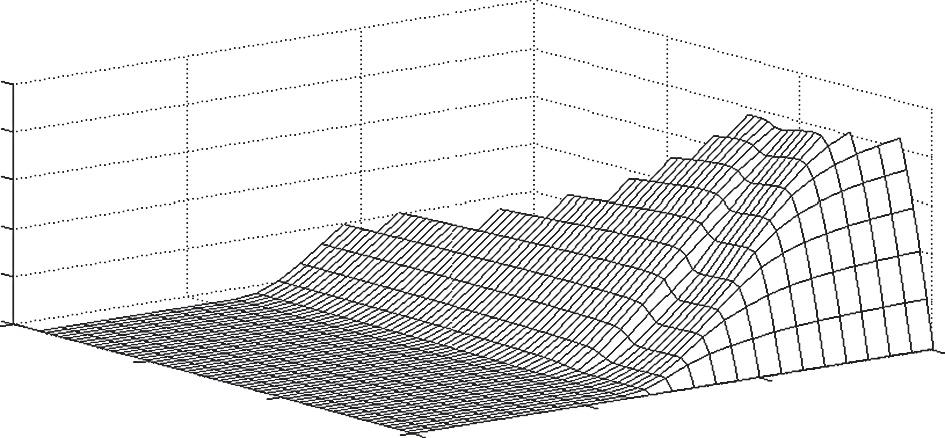
FIGURE1.2
Behaviorof ID(VDS, VGS)fora0.7 800 μm2 GaNHEMTat20°C.
Drain-source voltage (V) 051015202530
FIGURE1.3
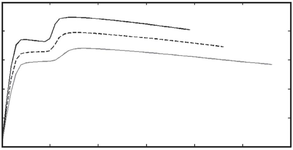
Outputcharacteristics ID(VDS)fora0.7 800 μm2 GaNHEMTat VGS ¼ 2Vunderthree differentambienttemperatures:20°C (solidblackline),50°C (dashedblackline),and80°C (solidgrayline)
onSiCsubstratewithagatelengthof0.7 μm[20].Toavoiddevicedegradation,the maximum VDS andthemaximumdissipatedpower Pmax havebeenlimitedto28V and5W/mm,respectively.Ascanbeobserved,thedeviceexhibitsanegativeslope of ID(VDS)underhighlydissipatedpowerconditionsbecauseoftheself-heating phenomenon.
Figure1.3 reports ID(VDS)at VGS ¼ 2Vunderthreedifferentambienttemperatures:20°C,50°C,and80°C.Itisobservedthattheself-heatingeffectisenhancedat highertemperaturesanddissipatedpower,duetotheassociatedincreaseofthephononscatteringprocessesleadingtoadegradationoftheelectrontransportproperties. Furthermore, Figure1.4 showstheloadlinesat1dBgaincompressionata fundamentalfrequency f0 of2GHzunderthethreeambienttemperatures.
20 10 0 VDS (V) VGS (V) I D (mA) 6 4 2 0 30 0 100 200 300 400 500
0 50 100 150 200 250
Drain current (mA)
5 1.2 Microwavetransistortechnologies
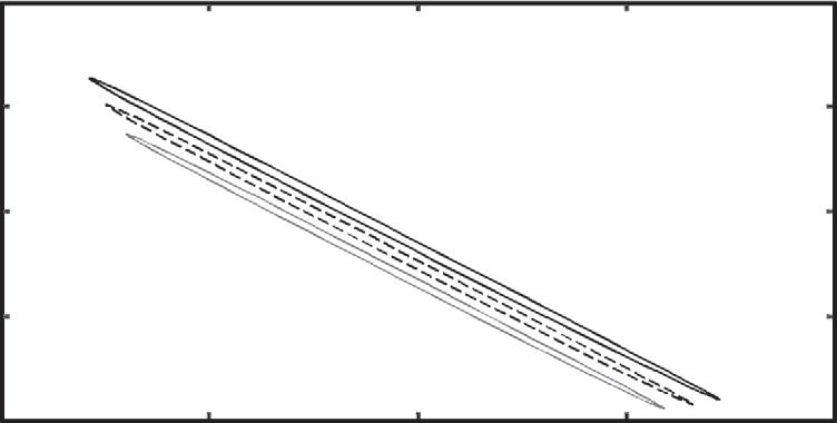
FIGURE1.4
Loadlinesat1dBcompressionwithafundamentalfrequencyof2GHzfora0.7 800 μm2 GaNHEMTat VGS ¼ 2Vand VDS ¼ 19.5Vunderthreedifferentambienttemperatures: 20°C (solidblackline),50°C (dashedblackline),and80°C (solidgrayline)
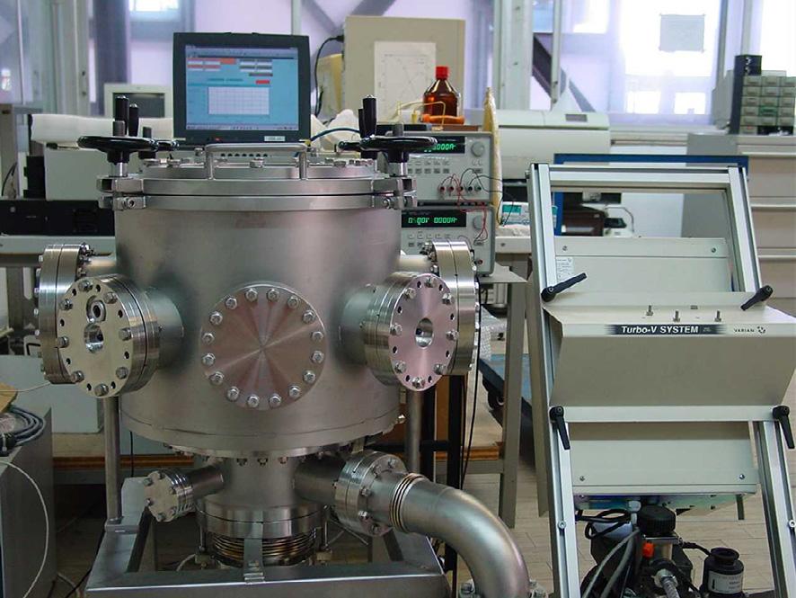
FIGURE1.5
Cryogenicsystemformicrowavetransistorcharacterization.
Asexpected,theswingoftheloadlinedecreasesathighertemperaturesandthis impliesareductionoftheoutputpower.
Figure1.5 showsapictureofanexperimentalset-upformicrowavetransistorcharacterizationatcryogenictemperatures.Thecryogenicsystemisbasedonaclosedcircleliquidheliumrefrigeratorandavacuumchamberhavingmicrowavecoaxial feedthroughsforconnectingtheexternalinstrumentation.Thetemperatureismonitoredandcontrolledbyusingaproportional-integral-differentialcontrolloop.ToillustratetheperformanceofacryogenicallycooledHEMT, Figure1.6 showsthebehavior ofthemagnitudeoftheforwardtransmissionparameterS21 forapackagedAlGaAs/ InGaAs/GaAspHEMT(MitsubishiMGF4919)versusfrequencyand VGS attwo differenttemperatureconditions:16.85°Cand 243.15°C[3].Bycoolingthe
400 300 200 100 0 1015202530 Drain-source voltage (V) Drain current (mA)
6CHAPTER1 Microwavetransistormodeling
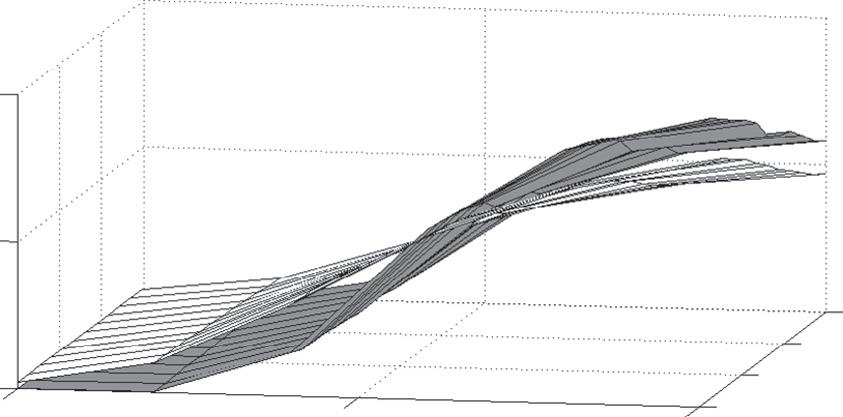
FIGURE1.6
Magnitudeof S21 versusfrequencyand VGS foraGaAspHEMT(MitsubishiMGF4919) at VDS ¼ 2Vundertwodifferentambienttemperatures:16.85°C (whiteplot) and 243.15°C (grayplot).
transistor,themagnitudeof S21 increaseswhen VGS isfarfrompinch-off,whileit decreaseswhen VGS isnearpinch-off.Theobservedbehaviorofthisfigureofmerit isduetothefactthat,bydecreasing VGS towardsthepinch-off,thethresholdvoltage (VTH)shifthasastrongerimpacton S21 thantheimprovementoftheaverageelectron velocity.Itshouldbeemphasizedthattheinfluenceofthethresholdvoltageshifton S21 mightbecompensatedbytheDCbiascircuitrywhenthedeviceisbiasedbyimposing ID ratherthan VGS [21].Itshouldbenotedthatexceptforthisdeviceinapackage,allof thetransistorsanalyzedinthischapterareon-waferdevices.
1.3 TRANSISTORMODELING
Whatismicrowavetransistormodeling?Itconsistsofthefieldofknowledgeand problem-solvingconcernedwithhowtoextract,implement,andvalidatemodels abletodescribethepropertiesofadvancedtransistorsmeantforhigh-frequency applications.Itisworthpointingoutthattheextractedmodelshavetobeproperly implementableinacircuitsimulatorandbeaccuratelyvalidatedbymeansofsuitable measurementspriortotheirrelease.Theimportanceofthisresearchbranchcomes fromtheneedformodelsashelpfulfeedbacktotechnologistsforadvancingtransistorfabricationandasaneffectivetoolforcircuitdesignersoptimizingcircuitperformance.Althoughmanysuccessfulmodelingtechniqueshavebeendevelopedinthe lastdecades,microwavetransistormodelingisanevergreenresearchfieldthatstill attractsextensiveinterest.Thisisbecauseinnovativetechniquesareconstantly requiredtomodelthelatestandcontinuouslyprogressingtransistortechnologies.
Asillustratedin Figure1.7,transistormodelscanbedividedintothreemaincategories:physicalmodels[22–25],behavioralmodels[26–29],andequivalentcircuit models[30–33].Thephysicalmodels(or“transparentboxes”)arebasedonthestudy ofthephysicalphenomenaoccurringwithinthetransistor,whilethebehavioral
10 5 0 –0.25 0 0 2 4 6 –0.5 | S 21 | VGS (V) Frequency(GHz)
7 1.3 Transistormodeling
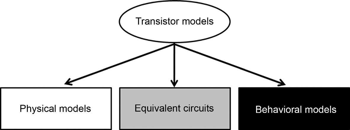
Classificationofthetransistormodelsintophysicalmodels(or transparentboxes),equivalent circuits(or grayboxes),andbehavioralmodels(or blackboxes).
models(or“blackboxes”)arebasedontheexperimentalcharacterizationofthe behavioralinput-outputdescriptionsofthetransistor.Aneffectivecompromise betweenphysicalandbehavioralmodelsisrepresentedbytheequivalentcircuits (or“grayboxes”),whichareextractedfromexperimentalmeasurements,yetkeeping theconnectionwiththeinnerphysicsofthetransistor.Equivalentcircuitmodelsgive thetechnologistsbetterfeedbackthanblack-boxmodelsandenablecircuitdesigners todomuchfastersimulationsthanwithphysicalmodels.Infact,physicalmodelsare notreallysuitableforcomputer-aideddesign(CAD)environmentsduetotheirprohibitivesimulationtime.Ontheotherhand,behavioralmodelsattransistorlevel requireexpensivemeasurementsandtheyshowgoodpredictivecapabilitiesonly intheregimeoftheircharacterization.Itisworthnotingthatbehavioralmodels atcircuitandsystemlevels,wherequiescentconditionandimpedanceenvironment (typically50 Ω)areaprioriknown,donotshowthesamelimitationspreviouslydiscussed,andhavebeensuccessfullyandincreasinglyusedbydesignersinthe lastyears.
Thepresentchapterfocusesonmicrowavetransistormodelingbasedonthe equivalentcircuitrepresentation.Equivalent-circuit-basedtransistormodelingis aninterdisciplinaryscientificresearchfieldthatrequiresexpertisefromdifferent areas:semiconductordevicephysics,electromagneticfields,microwavemeasurementtechniques,circuitnetworktheory,andcircuitsimulationsoftwarepackages. Althoughthemicrowaveperformanceofatransistorcanbefullyandstraightforwardlycharacterizedbycarryingouthigh-frequencymeasurementswithdedicated instrumentations,itisveryusefultoextractanequivalentcircuitmodel,asitisa physicallymeaningfulandaverycompactrepresentation,alsoallowingafastestimationofthescalingofthedeviceperformance.
Theselectionoftheappropriatetopologyoftheequivalentcircuitformodeling thespecifictestedtransistorisachallengingtask,sinceahighernumberofcircuit elementsmayallowforobtainingmoreaccurateresults,butthecircuitcomplexity becomeshigheraswellastheriskofphysicalinconsistency.Hence,thenumberof circuitelementsshouldbetherighttrade-offbetweenmodelaccuracy,physical
FIGURE1.7
8CHAPTER1 Microwavetransistormodeling
soundness,andcomplexity.Typically,thefirstmodelingstepconsistsofextractinga small-signalequivalentcircuitthat,subsequently,canbeusedasacornerstonefor buildingbothnoiseandlarge-signalmodels.Theremainderofthischapterisdedicatedtosmall-signal,noise,andlarge-signalmodeling.GaAsandGaNHEMTsare usedasreferencedevicestoillustratetheapplicationofequivalentcircuitmodeling techniqueswithexperimentalresults.
1.4 SMALL-SIGNALMODELING
Figure1.8 showsanexampleofasmall-signalequivalentcircuittopologyfora HEMT.Theresistances Rgsf and Rgdf areoftenomittedastheconductiongatecurrent isnegligibleundertypicaloperatingbiasconditions.Typically,thevaluesoftheelementsaredeterminedusingscattering(S-)parametermeasurements,whichcanbe straightforwardlyandaccuratelymeasuredbymeansofavectornetworkanalyzer (VNA).Givenabiascondition,themodelextractionisbasedondefiningeightequationsthatrepresentthefourcomplex S-parametersintermsoftheequivalentcircuit elementsateachfrequency.Severaltechniqueshavebeendevelopedtosolvethisillconditionedproblemandtheycanbeclassifiedintotwomaincategories:numerical optimization[34–36]andanalyticaltechnique[33,37,38].However,itiswellknown thatoptimizationmethodscanleadtocircuitelementvalueswithnophysicalmeaningandbywhichtheresultscandependonmanyfactors(eg,thestartingelement values,localminima,andtheoptimizationmethoditself).Ontheotherhand,analyticalmethodsallowovercomingthesedrawbacksbysplittingthemodelextraction intwoparts.Basically,theequivalentcircuitelementsareusuallydividedinto twomaingroups:theextrinsicelements(ie, Cpg, Cpd, Lg, Ls, Ld, Rg, Rs, Rd)andintrinsicones(ie, Cgs, Cgd, Cds, Rgsf, Rgdf, Rgs, Rgd, Rds, gm, τ ).Theformerareassumed
circuit
FIGURE1.8
Intrinsic
Rgdf Cgd Rgd Rds Rs Ls Source Cds Rd Ld Drain Cpd Rgsf Rgs Cgs gm V V + –e –jwt Rg Lg Cpg Gate
Small-signalequivalentcircuitforaHEMT. 9 1.4 Small-signalmodeling
tobebias-independent,whereasthelatteraredependentonthebiascondition.The analyticaltechniquesarebasedondeterminingfirsttheextrinsicelementsandsuccessivelytheintrinsicones.
Generally,theextrinsicelementsareobtainedfrom“cold” S-parametermeasurements(ie, VDS ¼ 0V)[33,37–48],becausethe“cold”conditionallowsasignificant simplificationoftheequivalentcircuitmodel.Theterm“cold”arisesfromthefact thattheequivalenttemperature,representingthecarrieraveragekineticenergy,is coldcomparedtothetypicaloperatingconditionandthedissipatedpowerisnull. With VDS equaltozero,thevoltagecontrolledcurrentsourcecanbeomittedsince therearenocarriersdriftingfromsourcetodrain.Asaresult,twounknowns(ie, gm and τ )disappearbut,atthesametime,twoequationsvanish(ie, S12 ¼ S21),duetothe factthatundercoldconditionthetransistorbehavesasareciprocalnetworkwith [S] ¼ [S]T (ie,notcontaininganynonreciprocalmediasuchasferritesorplasmas, oractivedevices).Additionally,thezerodrain-sourcevoltageallowsassumingthat thegate-sourceandgate-drainintrinsiccircuitsareequal. Figure1.9 showsthatthe intrinsiccoldHEMTcanberepresentedbyan RC parallelnetwork(Ry, Cy)modeling theSchottkygatejunctionandtwoidentical RC parallelnetworks(Rch/2,2Cch) modelingtheactivechannel.Astheintrinsicresistancesdecreaseathigher VGS, theintrinsiccapacitancesarenegligibleunderforwardcondition,whereastheintrinsicresistancesarenegligibleunderpinch-offcondition[40].Ingeneral,theextrinsic capacitancesareextractedfromIm(Yij)ofthecapacitivenetworkrepresentingthe
FIGURE1.9 Small-signalequivalentcircuitfora“cold”HEMT.
Source Intrinsic cold circuit Drain Gate Pinch-off Forward Cpg Cpd Cy Cy Rs Ry Ry Rg Rd Rch/2 Rch/2 Rch/2 Rch/2 2Cch 2Cch 2Cch 2Cch Ls Lg Ld
10CHAPTER1 Microwavetransistormodeling
transistoratlowfrequenciesunderpinch-offcondition,whereastheextrinsicinductancesandresistancesare,respectively,obtainedfromRe(Zij)andIm(Zij)of theresistiveinductivenetworkrepresentingthetransistorathighfrequenciesunder high VGS.
Afterde-embeddingtheextractedextrinsiccontributionsfromthe S-parameter measurementswithsimplematrixmanipulations[49],theintrinsicelementscan becalculatedfromtheintrinsic Y-parameters.Inparticular, Rgsf and Rgdf areestimatedfromtherealpartoftheintrinsic Y11 and Y12 atlowfrequenciesbyassuming thatthecapacitancesbehaveasopencircuits[50]:
Therefore,theextractedvaluesof Rgsf and Rgdf canbesubtractedand,finally,the remainingeightintrinsicelementscanbecalculatedfromtherealandimaginary partsofthefour Y-parameterswithstandardformulas[51].Itshouldbehighlighted that Rgsf and Rgdf playasignificantroleonlyatrelativelyhigh VGS whenforward biasingthegateSchottkyjunction.Thisisconfirmedby Figure1.10 showingthebias
Behaviorof Ggsf (A)and Ggdf (B)versus VDS and VGS fora0.2 100 μm2 GaNHEMT.
Rgsf ¼ 1 Re Y11 + Y12 ðÞ (1.1) Rgdf ¼ 1 Re Y12 ðÞ (1.2)
1 0.5 0 2 0 –5 –10 10 5 0 VGS (V) VDS (V) G gsf (mS) (A) G gdf (mS) VGS (V) VDS (V) 1 1.5 0.5 0 2 0 –5 –10 10 5 0 (B)
FIGURE1.10
11 1.4 Small-signalmodeling
dependenceofthetwoconductancesassociatedto Rgsf and Rgdf foraGaNHEMTon sapphiresubstratewithagatelengthof0.2 μm.
Itisworthnotingthattheanalysisoftheintrinsic Y-parametersversusfrequency cansuggesttoaddand/ortoneglectsomeintrinsiccircuitelements.Infact,differencesamongtechnologies,materials,structures,andstudiedfrequencyrangesare reflectedindifferentequivalentcircuittopologies.Forinstance,thepresentanalysis isfocusedontheintrinsic Y22 tohighlighttheimportanceofdeterminingthemost appropriatecircuittopology.Thepresenceofthefeedbackresistance Rgd allows definingthisadmittanceparameterasfollows:
Then,therealandimaginarypartsoftheintrinsic Y22 canbeexpressedasfollows:
Eq. (1.4) showsthat Rgd hastobeincludedinthemodelwhenRe(Y22)tendsto increasewithfrequencyinsteadofremainingconstantandequalto gds.Contrary tothebehaviorpredictedbyEq. (1.4), Figure1.11 showsthattheintrinsic Re(Y22)decreasesathigherfrequenciesforaGaAspHEMTwithagatelengthof 0.25 μm.Consequently,tomodelthisobservedbehavior, Rgd hasbeenomitted and gds hasbeenreplacedbyavoltagecontrolledcurrentsourcewithatimedelay τ ds.Thatsolutionallowsdefining Y22 asfollows[41]:
Hence,therealandimaginarypartsoftheintrinsic Y22 aregivenby:
Eq. (1.7) showsthat τ ds isrequiredtomodelthedecreaseofRe(Y22)athigherfrequencies(see Figure1.11).When ωτ ds issufficientlysmall, τ ds canbeapproximated withaninductance Lds inserieswith gds.However,incontrastwiththe Lds implementation, τ ds allowsthesimulationalsoofnegativevaluesofRe(Y22)[41].
Toverifytheaccuracyoftheextractedequivalentcircuit,themodelshouldbeable toreproducethe S-parametermeasurements.Furthermore,therobustnessofthemodel shouldbeconfirmedbyitsvalidationunderawiderangeofoperatingconditions. Inparticular,thecircuitelementsareexpectedtobephysicallymeaningfulandthus theirvaluesshouldbeanalyzedversusbiascondition,temperature,andgeometrical dimensionstocheckifthemodelmeetsthephysicalexpectations.Asanillustrative example, Figure1.12 reportsthegoodagreementbetweenmeasuredandsimulated
Y22 ¼ gds + jωCgd 1+ jωRgd Cgd + jωCds (1.3)
Re Y22 ðÞ¼ gds + ω2 Rgd C2 gd 1+ ωRgd Cgd 2 (1.4) Im Y22 ðÞ¼ ωCgd 1+ ωRgd Cgd 2 + ωCds (1.5)
Y22 ¼ gds e jωτ ds + jωCgd + jωCds (1.6)
Re Y22 ðÞ¼ gds cos ωτ ds ðÞ (1.7) Im Y22 ðÞ¼ ω Cgd + Cds gds sin ωτ ds ðÞ (1.8)
12CHAPTER1 Microwavetransistormodeling
Y 22 ) (mS) Frequency (GHz) 4 2 0 –2 0102030405060708090 0
FIGURE1.11
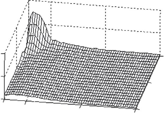
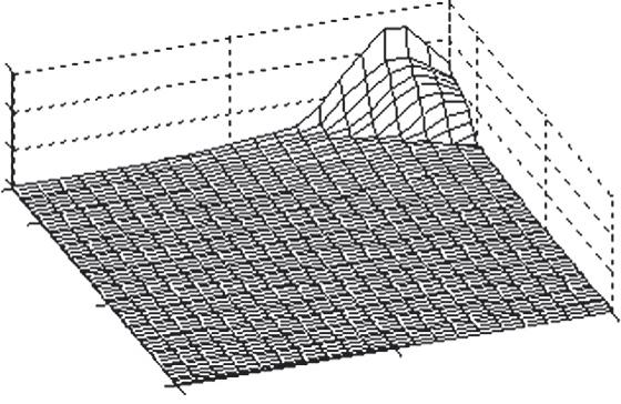
Comparisonbetweenmeasured (symbols) andsimulated (lines) intrinsic Y22 from4to 90GHzfora0.25 300 μm2 GaAspHEMTat VGS ¼ 0.65Vand VDS ¼ 10V.Simulationsare obtainedwith(A)andwithout(B)accountingfor τ ds
S-parametersforaGaAspHEMTwithagatelengthof0.15 μm[52].Thevalidationis performedunderdifferentbiasconditionsincludingnegative VDS,becausethetested deviceismeantforcold-FETmixerdesign.Itshouldbehighlightedthatthestandard formulasforidentifyingthecurrentsourceatpositive VDS havetobemodifiedforthe extractionatnegative VDS:thesignof gm hastobechangedandthis π phaseshifthasto besubtractedbeforecalculating τ .Theachievedbiasdependenceof gm and Cgs is reportedin Figure1.13.
Figure1.14 shows gm and Cgs versus VGS foraGaAspHEMTat VDS ¼ 2Vunder twodifferenttemperatureconditions:16.85°Cand 243.15°C[4].Inagreement withtheobservedbehaviorofthemagnitudeof S21 (see Figure1.6),thetesteddevice showsthattheimprovementofthecarriertransportpropertiesatcryogenictemperatureleadstoanincreaseof gm onlywhen VGS isfarfrompinch-off.With VGS 4 2 0 0102030405060708090 –2 0
lm(
Re(
60 lm( Y 22
(mS) Re( Y 22
(mS)
(A) (B)
20 40 60
Y 22 ) (mS)
20 40
)
)
Frequency (GHz)
13 1.4 Small-signalmodeling
FIGURE1.12
Comparisonbetweenmeasured (symbols) andsimulated (lines)S-parametersfrom2.5to 65GHzfora0.15 300 μm2 GaAspHEMTat: VDS ¼ 0Vand VGS ¼ 1V(A), VDS ¼ 0.5Vand VGS ¼ 0.8V(B), VDS ¼ 0.5Vand VGS ¼ 0.5V(C).
S
S
–
12 S
S
2
S
6
(A) (B) (C)
22 S21
11
S
22 S21/3
11
× S12
22 S11 S21
× S12
14CHAPTER1 Microwavetransistormodeling
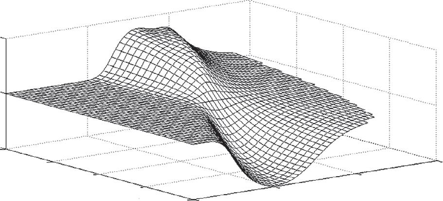
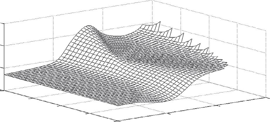
FIGURE1.13
Behaviorof gm (A)and Cgs (B)versus VDS and VGS fora0.15 300 μm2 GaAspHEMT.
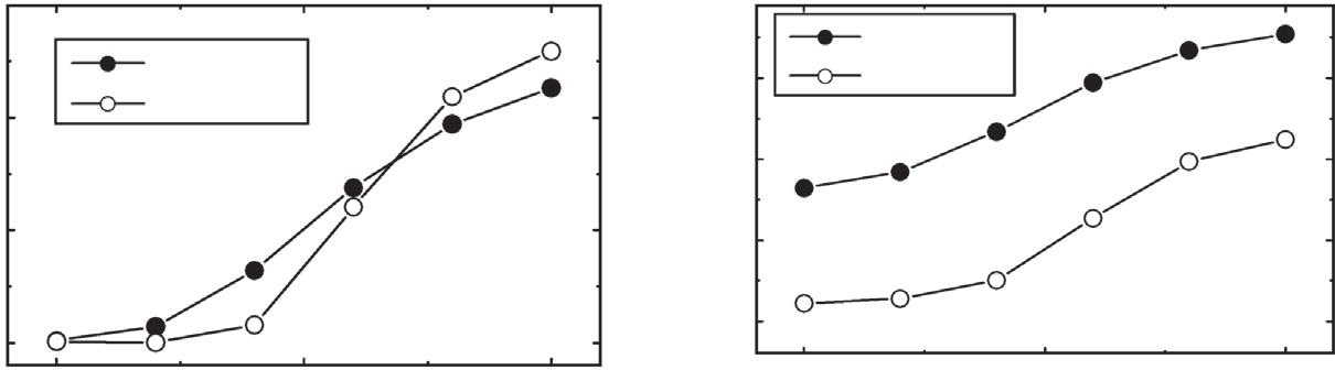
FIGURE1.14
Behaviorof gm (A)and Cgs (B)versus VGS foraGaAspHEMT(MitsubishiMGF4919) at VDS ¼ 2Vundertwodifferentambienttemperatures:16.85°C (blacksymbols) and 243.15°C (whitesymbols)
decreasingtowardsthepinch-offregion,the VTH shiftleadstoadegradationof gm at lowertemperatures.Sucha VTH shiftcanbeattributedtothereductionofthenet positivechargeunderthegate,duetoadecreaseofthethermallyactivatedelectron detrappingmechanismsoccurringwithintheAlGaAsdonorlayer.Asaresultofthis reductionofthedetrappingphenomena,adecreaseofthe“equivalent”dopinglevel canberesponsiblefortheobservedreductionof Cgs atlowertemperatures[4].
200 –200 0 0.8 0.4 –0.4 –0.8 –2 –1 0 1 0 V DS (V) V GS (V) g m (mS) (A) 200 100 300 0 0.8 0.4 –0.4 –0.8 –2 –1 0 1 0 V DS (V) V GS (V) C gs (fF) (B)
150 100 50 0 –0.50 –0.25 0.00 T = 290 K T = 30 K g m (mS) V GS (V) T = 290 K T = 30 K 400 300 350 250 –0.50 –0.25 0.00 V GS (V) C gs (fF) (A)(B)
15 1.4 Small-signalmodeling
Theconventionalscalingrulesarebasedontheassumptionthatincreasingthe gatewidthcanbeseenasconnectingmoreintrinsictransistorsinparallel.Hence, theintrinsicequivalentcircuitelementsassociatedwithadmittances(ie,capacitancesandconductances)andthedraincurrentitselfshouldbeproportionalto thetotalgatewidth,whiletheintrinsiconesassociatedwithimpedances(ie,inductancesandresistances)shouldbeinverselyproportionaltothisgeometricdimension,andtheintrinsictimedelayshouldbeconstant.Nevertheless,thisisan oversimplifiedassumptionthatfailstotakeintoaccountcomplexphenomenasuch asthermaleffects,bordereffects,andresidualextrinsicelementcontributions.As illustrativeexample, Figure1.15 shows g
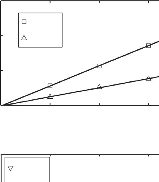
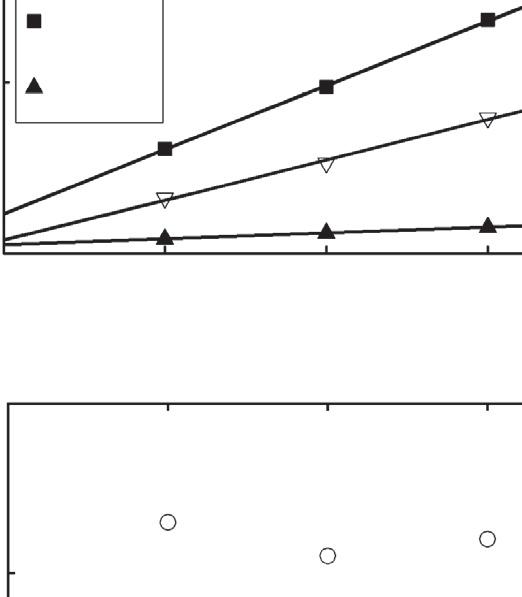
FIGURE1.15
Behaviorof gm, gds (A), Cgs, Cgd, Cds (B),and τ (C)versusthegatewidthforthreeGaAs HEMTs(0.25 100 μm2,0.25 200 μm2,and0.25 300 μm2)at VGS ¼ 0.6Vand VDS ¼ 2.5V.
m, gds,
gs,
gd,
ds,and
150 100 50 0 0100200300400 W (μm) g (mS) g m 10 × g ds 400 200 0 0100200300400 W (μm) C (fF) Cgs Cgd 0.5 × Cds 2 1 0 0100200300400 t ( ps ) W (μm) (A) (B) (C)
C
C
C
τ versusthegate
16CHAPTER1 Microwavetransistormodeling
widthforthreeAlGaAs/GaAsHEMTswithagatelengthof0.25 μm.As expected,aquiteclearlinearbehaviorw ithrespecttothegatewidthisobserved in gm, g ds , Cgs , C gd ,and C ds ,while τ isalmostindependentofthegatewidth. Thisisbecause τ canbecorrelatedtothecarrie rtransittimeand,therefore, dependsmainlyonthegatelength(infirs tapproximation,proportionally).As canbeseenin Figure1.16A ,thelineapproximating gm versusthegatewidth exhibitsapositiveinterceptwhen V GS isincreasedto0V.Thisresultcanbe attributedtothefactthatthethermalphenomenaareenhancedintransistorswith largergatewidthandathigher V GS ,duetothehigherdissipatedpower.Tocorroboratethisobservation, g m isnormalizedwithrespecttothegatewidthin Figure1.16B andtheachievedvalueisevidentlyreducedinlargertransistors. Byconsideringthatthethermalphenomenacannotfollowtheappliedsmallsignalatsuchhighfrequencies,theobserveddegradationofthenormalizedRF g m hastobeascribedtotheeffectsofthermalphenomenaduetotheDC dissipatedpower.
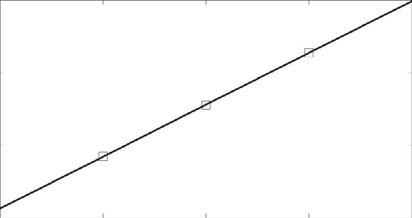
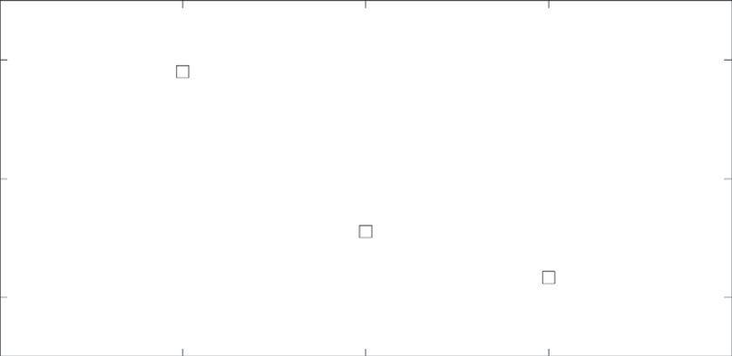
FIGURE1.16
Behaviorof gm (A)anditsnormalizedvalue(B)versusthegatewidthforthreeGaAsHEMTs (0.25 100 μm2,0.25 200 μm2,and0.25 300 μm2)at VGS ¼ 0Vand VDS ¼ 2.5V.
0 0 20 40 60 100200 W (µm) 300400 g m (mS) (A) 0 150 160 g m (mS/mm) 170 100200 W (μm) 300400 (B)
17 1.4 Small-signalmodeling