LINES WITH SMART STORAGE SOLUTIONS THAT WORK WITH ERP AND MES SYSTEMS
Hawker Richardson and Scienscope have been partnering to supply component storage solutions to manufacturers in Australia. The storage solutions consist of a range of solutions from Reel Management, X-ray Component Counting, and Goods Received Component Management. Component management supporting the Industry 4.0. ethos
All manufactures in Australasia driving their production towards Industry 4.0. and operating at a smarter level with increased automation and efficiency have been investing in component management.
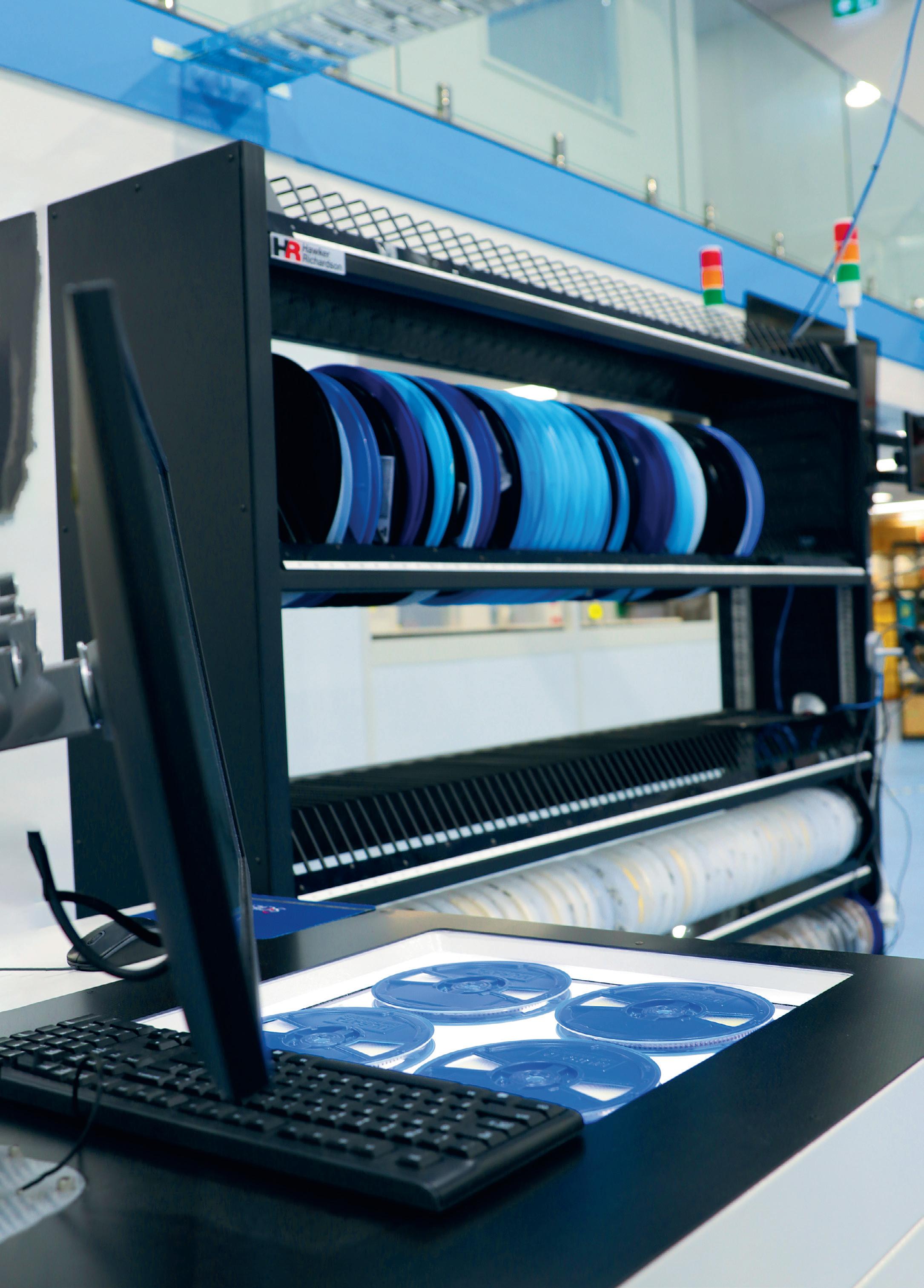
Reel Management — Smart Racks
Smart racks are available for both reels and stencils. The storage solution incorporates sensors on each position so you can easily keep track of inventory with unique ID numbers for each component, enabling FIFO/FEFO retrieval from their designated storage locations.
Features such as automatic reel placement, removal detection, and multi-colour LEDs for simultaneous multi-kitting, ensures optimal efficiency in production operations.
IMS-100 Receiving Station
The semi-automatic receiving station is ideal for goods-in where you streamline your incoming material process and eliminate any human error mistake from data entry to relabelling. The high-resolution camera of the IMS100 with image-based algorithm reads any barcode type and even characters which can be uploaded to MES/ERP Systems.
X-ray Component Counting
With state-of-the-art X-ray technology and intelligent AI algorithms, the AXC-800III captures high-quality images of components inside reels and utilizes AI to count material accurately. With an exceptional accuracy and repeatability rate of 99.99%, the AXC-800 III can count down to 01005 in less than two seconds per reel. Hawker Richardson www.hawkerrichardson.com.au
THERMAL CHALLENGES UNDERSTANDING
IN EV CHARGING APPLICATIONS
Jeff Smoot, VP of Apps Engineering and Motion Control, CUI Devices
While the concept of electric vehicles (EVs) has been around for as long as gasoline vehicles, it’s only in recent years that they’ve gained widespread acceptance.
This surge in popularity can be attributed to significant advancements in EV technology coupled with substantial governmental backing. For instance, the European Union’s decision to ban internal combustion vehicles by 2035 and mandate fast EV charging stations every 60 kilometres by 2025 serves as a clear testament to this anticipated surge in demand.
As EVs emerge as the dominant mode of transportation, factors such as battery range and even quicker charging rates will play pivotal roles in sustaining the global economy. Enhancements in EV charging infrastructure will necessitate advancements across various domains, with thermal management standing out as a key area requiring technological evolution.
AC and DC EV chargers — what’s the difference?
As the demand for quicker charging solutions intensifies, there have been both incremental and transformative shifts in approach. One
notable change is the increasing adoption of DC chargers — a term that may initially seem ambiguous given that all battery systems inherently operate on DC electricity. However, the crucial distinction lies in where the conversion from AC to DC occurs within these systems.
The conventional AC charger, typically encountered in residential settings, primarily serves as a sophisticated interface responsible for communication, filtering and regulating the flow of AC power to the vehicle. Subsequently, an onboard DC charger within the vehicle rectifies this power and charges the batteries. In contrast, a DC charger undertakes rectification prior to delivering power to the vehicle, transmitting it as a high-voltage DC source.
The primary advantage of DC chargers lies in their ability to eliminate many constraints related to weight and size by relocating the power conditioning components from the EV to an external structure.
By shedding weight and size constraints, DC chargers can seamlessly incorporate ad-
ditional components to enhance both their current throughput and operating voltage. These chargers leverage state-of-the-art semiconductor devices for rectifying power, alongside filters and power resistors, all of which generate substantial heat during operation. While the contributions of filters and resistors to heat dissipation are noteworthy, the predominant heat emitter in an EV charging system is the insulated gate bipolar transistor (IGBT), a semiconductor device that has witnessed increased adoption in recent decades. This robust component has unlocked numerous possibilities in the charging domain, yet ensuring its adequate cooling remains a significant concern.
Tackling heat challenges
An IGBT essentially serves as a hybrid between a field-effect transistor (FET) and a bipolar junction transistor (BJT). Renowned for their capacity to endure high voltages, minimal onresistance, rapid switching rates and remarkable
thermal resilience, IGBTs find optimal utility in high-power scenarios such as EV chargers.
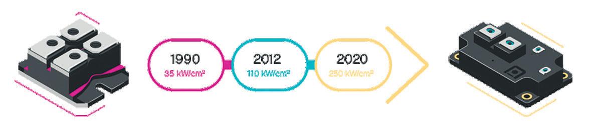
In EV charging circuits, where IGBTs serve as rectifiers or inverters, their frequent switching operations lead to the generation of significant heat. Presently, the foremost thermal challenge pertains to the substantial escalation in heat dissipation associated with IGBTs. Over the past three decades, heat dissipation has soared more than tenfold, from 1.2–12.5 kW, with projections indicating further increases. Figure 2 below illustrates this trend in terms of power per unit surface area.
To put this into perspective, contemporary CPUs achieve power levels around 0.18 kW, corresponding to a modest 7 kW/cm2. The staggering disparity underscores the formidable thermal management hurdles facing IGBTs in high-power applications.
Two contributing factors play significant roles in enhancing the cooling of IGBTs. Firstly, the surface area of IGBTs is approximately twice that of CPUs. Secondly, IGBTs
can withstand higher operating temperatures, reaching up to +170°C, whereas modern CPUs typically operate at only +105°C.
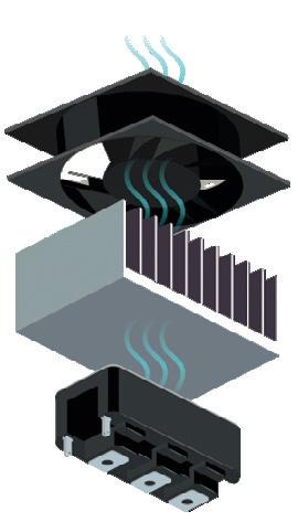
The most effective method for managing thermal conditions involves employing a combination of heatsinks and forced air. Semiconductor devices, such as IGBTs, generally exhibit extremely low thermal resistance internally, while the thermal resistance between the device and the surrounding air is comparatively high. Incorporating a heatsink substantially increases the available surface area for dissipating heat into the ambient air, thereby reducing thermal resistance. Additionally, directing airflow over the heatsink further enhances its efficacy. Given that the device–air interface represents the most significant thermal resistance in the system, minimising it is crucial. The advantage of this straightforward approach lies in the reliability of passive heatsinks and the well-established technology of fans.
CUI Devices has customised heatsinks specifically for EV charging applications, with dimensions of up to 950 x 350 x 75 mm. These heatsinks are capable of passively handling less demanding requirements or actively managing more demanding scenarios with forced air.
In addition to air cooling methods, liquid cooling offers an alternative for dissipating heat from high-power components like IGBTs. Water-cooling systems are attractive due to their ability to achieve the lowest thermal resistances. However, they come with higher costs and increased complexity compared to air cooling solutions. It’s also worth noting that even in water-cooling setups, heatsinks and fans are still essential components for effective heat removal from the system.
Considering the associated costs and complexities, direct cooling of IGBTs using heatsinks and fans remains the preferred approach. Ongoing research efforts are focused on enhancing air cooling technologies
specifically tailored for IGBT applications. This active research aims to optimise heat dissipation while minimising costs and system complexities associated with liquid cooling methods.
Thermal system design considerations
The effectiveness of any cooling system relies heavily on the strategic placement of components to optimise airflow and enhance heat distribution. Insufficient spacing between components can impede airflow and limit the size of heatsinks that can be utilised. Therefore, it’s crucial to strategically position critical heat-generating components throughout the entire system to facilitate efficient cooling.
In addition to component placement, the positioning of thermal sensors is equally vital. In large-scale systems like DC EV chargers, real-time temperature monitoring facilitated by control systems plays a crucial role in active thermal management. Automatic adjustments in cooling mechanisms based on temperature readings can optimise system performance and prevent overheating by regulating current output or adjusting fan speeds. However, the accuracy of these automatic adjustments is contingent upon the quality and precision of the temperature sensors. Poor placement of sensors can lead to inaccurate temperature readings, resulting in ineffective system responses. Therefore, careful consideration must be given to the placement of thermal sensors to ensure the accuracy and reliability of temperature monitoring and control.
Environmental factors
EV charging stations are frequently deployed in outdoor environments, subject to diverse weather conditions. Therefore, designing weather-resistant enclosures with proper ventilation and protection against elements, such as rain and extreme temperatures, is imperative to uphold optimal thermal performance. It’s crucial to ensure that airflow paths and venting systems are engineered to prevent water ingress while maintaining unobstructed airflow.
Among external factors, solar heating from direct sunlight poses a significant challenge, leading to a considerable increase in the internal ambient temperature of the charger enclosure. While this presents a legitimate concern, the most efficient solution is relatively straightforward. Implementing well-designed shading structures with sufficient airflow between the shading and the charging unit
effectively mitigates solar heating, thereby maintaining lower ambient temperatures within the charger enclosure.
What’s next?
In recent years, there has been a remarkable surge in the worldwide adoption of electric vehicles, with demand showing consistent and significant growth across various technological fronts. As the number of EVs on the road continues to escalate, the proliferation of charging infrastructure is expected to expand in lockstep. The effective operation and efficiency of chargers are paramount to the development of this burgeoning charging infrastructure. Cost-efficiency is also a critical factor, as the speed at which individuals and businesses integrate these chargers into their homes and establishments is contingent upon affordability.
Anticipating the continuous growth of EVs and chargers, one must acknowledge the evolving nature of the underlying technologies. This entails considering potential advancements in
charging power and capacity, evolving software and hardware standards, and allowing room for unforeseen innovations. This proactive approach ensures that thermal management systems can adapt to evolving demands over time.
At their core, electric vehicle chargers share similar thermal management concerns with other dense, high-power electronic devices. However, the power density of the insulated-gate bipolar transistors (IGBTs) utilised in EV chargers, coupled with the escalating demands placed on them, presents a unique challenge. As charging speeds and battery capacities continue to rise, the imperative to develop chargers effectively and safely becomes increasingly stringent, demanding more from thermal management designers and engineers than ever before.
CUI Devices offers a comprehensive range of thermal management components, coupled with industry-leading thermal design services, to support the evolving needs of the electric vehicle charging ecosystem.
Figure 2: The power density of IGBTs has experienced significant advancements.
Figure 3: Utilising heatsinks and fans represents a highly effective thermal management solution for IGBTs.
Figure 4: Shielding chargers from direct sunlight presents a cost-efficient and efficient strategy for managing thermal conditions.
Figure 1: DC chargers exhibit notably accelerated charging rates, albeit with heightened complexity and increased heat generation.
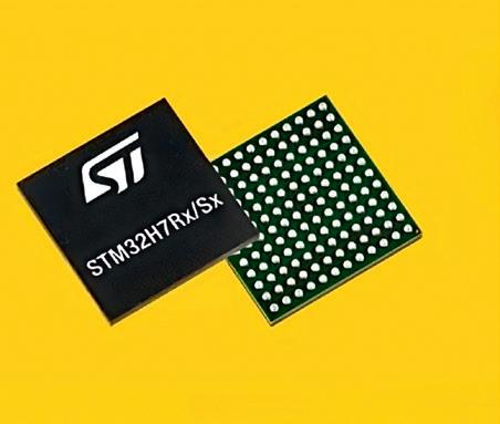
STM32H7R/S
Scalable and secure bootflash microcontrollers
• Arm® Cortex®-M7 running at up to 600 MHz, 1284 DMPIS
• Real-time execution from internal or external memories
• High-speed serial and parallel memory interfaces up to 200 MHz DTR
Data from the Graz University of Technology (TU Graz) indicates that approximately 1.2 million lithium-ion batteries of electric cars, buses and construction machinery will be decommissioned worldwide by 2030. Around 14 million discarded batteries are expected to be discarded by 2040. Recycling these materials makes sense, but as it can be expensive and technically demanding, it would be more sustainable to reuse the batteries, for example as stationary electricity storage units. However, this requires an assessment of their remaining performance capability and safety.
Jörg Moser (left) and Christian Ellersdorfer from the Vehicle Safety Institute at TU Graz.
usage profiles without having to rely on data that is sensitive in terms of data protection, like the usage history of the batteries. “On this basis, we can decide whether a battery is, in principle, suitable for further use in a particular area of application,” Moser said.
Now, researchers from TU Graz have established the first parameters that can be used to assess the condition of the discarded batteries. So far, the reduced charging capacity and an increase in internal resistance have served as indicators of the condition of a used battery. However, that is not sufficient for a decision on possible second-life use.
For this reason, the researchers analysed lithium-ion cells that had been used in vehicles under real conditions and identical new ones
in the laboratory. During repeated charging and discharging cycles, they recorded 31 different parameters and then checked how well they represented the aging condition of the batteries. 13 of these indicators turned out to be meaningful, including the charging and discharging capacity, the temperature difference between the poles during the charging process and the relaxation behaviour of the battery cell after the charging process.
Jörg Moser, head of the Battery Safety Centre Graz at the Vehicle Safety Institute at TU Graz, said the researchers used these indicators to draw conclusions about the aging status of lithium-ion batteries and different
However, the safety status of the batteries still needs to be assessed to ensure low-risk reuse. In the course of their first life, chemical changes occur in the batteries, which can affect their safe use. Christian Ellersdorfer, the head of the COMIT project SafeLIB at the Vehicle Safety Institute, said it is crucial to understand battery cells and the processes, reactions and changes that take place in them in order to determine their safety behaviour.
It could be several years before the batteries are reused on a broad basis in subsequent applications, making electromobility even more sustainable over its entire lifecycle. After all, new storage materials, the safety of different battery technologies, warranties and liability must also be taken into consideration.
“This results in an interdisciplinary field of research that we want to work on at TU Graz together with national and international partners in further research projects,” Ellersdorfer said.
A NEW CLASS OF SILICON SYSTEMS FOR AI CONNECTED DEVICES
Researchers from the National University of Singapore have demonstrated a new class of silicon systems that could enhance the energy efficiency of AI connected devices. These technological breakthroughs could also enhance the capabilities of the semiconductor industry in Singapore.
The innovation was demonstrated in a fully-depleted silicon-on-insulator (FDSOI) and can be applied to the design and fabrication of advanced semiconductor components for AI applications. The new chip has the potential to extend the battery life of wearables and smart objects by a factor of 10, support intense computational workloads for use in Internet of Things applications and reduce the power consumption associated with wireless communications with the cloud.
Professor Massimo Alioto from the NUS College of Design and Engineering said IoT devices often operate on a limited power budget and therefore require low average power to efficiently perform regular tasks such as physical
signal monitoring. At the same time, high performance is needed to process occasional signal events with computationally intensive AI algorithms. “Our research allows us to simultaneously reduce the average power and improve the peak performance. The applications are wide-ranging and include smart cities, smart buildings, Industry 4.0, wearables and smart logistics,” Alioto said.
The research findings could also allow researchers to enhance the area of batterypowered AI devices, as they could move intelligence from conventional cloud to smart miniaturised devices. The research conducted by the NUS FD-SOI Always-on Intelligent & Connected Systems (FD-fAbrICS) joint lab revealed that the researchers’ FD-SOI chip
technology can be deployed at scale with enhanced design and system integration productivity for faster market reach and rapid industry adoption.
“This innovation has the potential to accelerate the time to market for key players in Singapore’s semiconductor ecosystem,” Alioto said.
Going forward, the researchers hope to facilitate the adoption and deployment of their design technologies at scale. This will enable the AI and semiconductor industry in Singapore to have a competitive advantage while reducing the overall deployment cost of FD-SOI systems. The NUS research team will now look into developing new classes of intelligent and connected silicon systems that could support larger AI model sizes (“large models”) for generative AI applications. The resulting decentralisation of AI computation from cloud to distributed devices will preserve privacy and avoid wireless data deluge under the simultaneous presence of a range of devices.
Lunghammer
TU Graz.
RESEARCH BREAKTHROUGH IN DATA CENTRE INTERCONNECTS
Data centres are designed to store, process and distribute vast amounts of data and applications. From ensuring data availability to supporting scalability, disaster recovery and maintaining robust security measures, data centres play a critical role in enabling the functioning of the modern interconnected digital landscape.
At the heart of data centre operations lie data centre interconnects, the networking infrastructure responsible for facilitating communication between various components within and across data centres. Digital-to-analog converters (DACs) are vital components within these interconnects, tasked with converting digital signals into analog signals for transmission over copper cables. However, the requirement for high-resolution DACs can pose a significant bottleneck due to the associated increase in costs of optical modules.
To address this challenge, researchers have presented a solution that combines a look-up-table-based nonlinear predistortion technique with digital resolution enhancement. This approach, reported in Advanced Photonics Nexus, aims to alleviate the limitations imposed by high-resolution DACs while maintaining efficient data transfer and communication within data centre interconnects.
The proposed technique has yielded remarkable experimental results; by employing look-up-table-based predistortion to mitigate nonlinear impairment, and digital resolution enhancement to reduce the demand for DAC resolution, the researchers have achieved exceptional data transmission performance.
The digital signal processing technique enabled the transmission of signals at rates exceeding 124 GBd PAM-4/6 and 112 GBd PAM-8 over 2 km of standard singlemode fibre using 3/3.5/4-bit DACs. It also facilitated the transmission of 124 GBd PAM-2/3/4 signals over 40 km of standard singlemode fibre using 1.5/2/3-bit DACs. These results represent an advancement in data centre interconnect technology, demonstrating the feasibility of supporting the next generation of Ethernet links targeting speeds of up to 800 GbE or potentially even 1.6 TbE.
Beyond enhancing data centre interconnects, these advancements could also transform various applications across 6G access networks and passive optical networks. By overcoming the challenges associated with high-resolution DACs, this innovative approach also paves the way for more efficient data transmission.
WEARABLE HEALTH SENSOR CHARGES WITHOUT WIRES OR BATTERIES
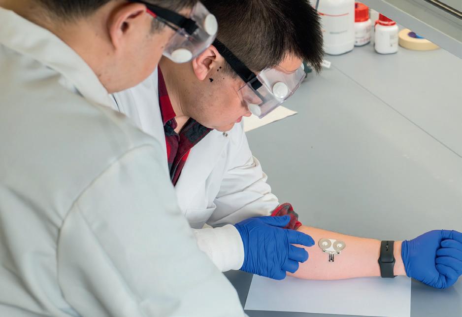
A team of researchers from the University of Missouri have made a breakthrough in their ongoing development of an on-skin wearable bioelectronic device. Associate Professor Zheng Yan’s lab, which specialises in soft bioelectronics, recently added a novel component to the team’s ultra-soft, breathable and stretchable material — wireless charging, without batteries, through a magnetic connection.
The innovation, detailed in Nature Nanotechnology, could help gather precise vital sign measurements like blood pressure, electrical heart activity and skin hydration. The discovery could also lead to early detection and timely interventions for chronic diseases such as heart disease, cancer and diabetes.
“A watch is a hard surface, so it’s not as effective as our material in providing accurate vital sign tracking. Our porous, soft material acts as an electrical conductor, so it can maintain a stable electrical current during movement. This is a significant step forward toward our overall goal to help improve the long-term biocompatibility and the long-lasting accuracy of wearable bioelectronics,” Yan said.
The researchers’ end goal is to provide people with a convenient, comprehensive health picture through long-term self-health monitoring, and the capability to share that information wirelessly with a person’s healthcare provider. Now, the researchers have overcome a significant challenge and created an accurate, wireless connection.
“If we can make affordable, customised electronics and equip our bodies with these devices, we can take proactive actions at the early stages of some diseased conditions and dramatically change and reshape our future,” Yan said.
While Yan’s material has significant on-skin capabilities, his team is also exploring the possibilities of integrating it with implanted devices like pacemakers. Because the implanted material does not require Bluetooth technology and is battery free, it has advantages over existing technology, making it suitable for safe and effective use in medical applications. “If a device made from our soft material can be put directly on the surface of the heart, we can get a more reliable and timelier signal, leading to early detection of this health issue,” Yan said.
The research builds on the team’s existing proof of concept, as demonstrated by their previous work, including a heart monitor currently under development.
Ganggang Zhao, left, demonstrates the device’s wireless charging capability as Zheng Yan observes the test.
Ben Stewart/University of Missouri.
STRATEGY DEVELOPED FOR ‘SELF-HEALING’ SOLAR CELLS
Researchers from Monash University, the University of Oxford and the City University of Hong Kong have developed a novel strategy to enhance the stability and performance of perovskite solar cells (PSCs). The next-generation solar cells could be able to withstand corrosive susceptibility by ‘self-healing’, in a breakthrough that could pave the way for more reliable perovskite solar cells that contribute to the global transition towards sustainable energy solutions.
Highly efficient, lightweight and cheap, PSCs are expected to play a leading role in the future of solar energy production, but scientists still need to make them more durable and figure out how to produce them on a larger scale. A study published in Nature has detailed the strategy that enhances the stability and performance of perovskite solar cells.
Professor Udo Bach, study co-author, said the research addresses the issues related to defect passivation in perovskites that have hindered the widespread adoption of this technology.
The innovative agent developed by Monash researchers heals the perovskite layer when exposed to environmental stressors such as moisture and heat. The researchers’ approach resulted in solar cells with 25.1% power conversion efficiency and remarkable stability under 1000 hours of accelerated ageing tests at 85°C and simulated solar illumination.
“Our slow-release strategy represents a significant advancement in the field of perovskite photovoltaics. By slowly releasing the passivating agents into our perovskite material, we have been able to produce solar cells not only with enhanced performance but also extended long-term stability under real-world conditions,” Bach said.
FANLESS PANEL PCs
Advantech has launched the PPC-415W and PPC-421W advanced panel PCs, designed to meet the needs of industrial environments.
The PPC-415W features a 15.6 ″ full HD display, while the PPC-421W has a larger 21.5 ″ full HD screen. Both models are powered by the latest 13th Gen Intel Core processors to provide computing power for a variety of applications. The fanless design is a key feature, reducing noise and increasing the system’s durability by eliminating the need for moving parts. This makes the PCs suitable for harsh industrial settings where dust and debris can pose challenges to traditional fan-cooled systems.
These new models also feature a wide operating temperature range. They can function in environments with temperatures ranging from -20 to 60°C, providing performance in both extremely hot and cold conditions. This flexibility makes them suitable for use in a range of industries, including manufacturing, automation and energy management.
The fanless panel PCs are equipped with rich connectivity options to enhance their versatility. They include multiple COM and USB ports, offering connectivity for peripheral devices. Additionally, the systems support various expansion options, allowing users to customise the PCs to meet specific operational needs. This adaptability allows the panel PCs to be integrated into existing workflows, enhancing overall productivity.
Both models are designed with a sleek exterior, with a robust build that makes them suitable for a range of industrial environments.
In conclusion, Advantech’s PPC-415W and PPC-421W fanless panel PCs represent an advancement in industrial computing technology. Their combination of a wide operating temperature range and extensive connectivity options make them a versatile solution for modern industrial applications.
Advantech Australia Pty Ltd www.advantech.net.au
ALUMINIUM ENCLOSURES
The METCASE UNIDESK sloping front aluminium enclosures are suitable for industrial/machine control and security/access control. They are also designed for a range of other applications including office systems, point-of-sale and medical devices.
The enclosure’s large front panel (accessory) is recessed for a membrane keypad. The flat rear panel can be machined to accommodate connectors, switches and power inlets. Pre-punched fixing points in the base make it easy to install PCBs.
The enclosures are available either in three standard widths — 200, 300, 400 mm (x 200 x 102 mm) — or in custom widths. The enclosures can be supplied either with or without an IP54 sealing gasket. For IP54 protection, PCB pillars (accessory) are also required.
The enclosures can be specified in two standard colours: light grey (RAL 7035) and black (RAL 9005). Custom colours are also available on request. The enclosures are supplied pre-assembled with four non-slip rubber feet, stainless steel M3 Torx T10 and MS M3 Posidrive fixings.
Accessories include front panels, wall mounting kits, a PCB mounting kit and M3 PCB/panel fixing screws.
Like all METCASE enclosures, UNIDESK can be supplied fully customised. Services include custom front panels, CNC machining, fixings and inserts, painting/finishing and digital printing of graphics, legends and logos.
ROLEC OKW Australia New Zealand P/L www.metcase.com.au
MICROCONTROLLERS
The STM32H7R and STM32H7S microcontrollers from STMicroelectronics can be used at 600 MHz and are suitable for integrators who require external storage. Additionally, while there’s less flash, the STM32H7R and STM32H7S support bootflash instead of the traditional boot ROM. Some also offer a NeoChrom GPU.
The general-purpose line, the STM32H7R3/S3, features a Chrom-ART accelerator for 2D graphics. It has been designed to help enhance graphical user interfaces by fetching assets from memory faster and accelerating operations like 2D copies, transparencies or alpha-blending. Consequently, Chrom-ART is designed to enable modern UIs on even the most constrained devices like smart watches and wearables.
The STM32H7R7/S7 features a NeoChrom GPU. The hardware IP is a 2.5D accelerator optimising texture mapping with bilinear and point sampling. It also accelerates animations and drawing operations, thereby helping to offload the Cortex-M7. The NeoChrom GPU also has an 8-bit Octal Serial Peripheral Interface (OSPI) or a 16-bit high-speed interface (HSPI) to fetch assets from the external memory modules faster and deliver them to the L2 cache.
STMicroelectronics Pty Ltd www.st.com
BLUETOOTH MODULE
Quectel Wireless Solutions has launched the HCM511S MCU Bluetooth module for compact connected devices such as digital keys, portable devices and battery-operated motion sensors. Utilising Bluetooth Low Energy 5.4, the module accommodates an ARM Cortex-M33 processor and features built-in 32 KB RAM and either 352 or 512 KB flash memory.
The module also features enhanced receiver sensitivity and a maximum transmit power of +6 dBm to facilitate long-distance transmission. Measuring 16.6 x 11.2 x 2.1 mm, the module is in the ultracompact LCC form factor in order to optimise size for end products. Suitable applications for the module include sports and fitness devices, PC peripherals and accessories, healthcare applications including blood pressure and glucose metering, indoor navigation, digital key, connected lighting control and smart home and smart building applications.
The module also offers the option of support for Bluetooth mesh network low-power nodes. This enables increased network scalability and node counts over mesh topology, enabling greater device density. The module offers up to 18 GPIOs which can be multiplexed for various interfaces including ADC, USART, I2C, I2S, SPI and PWM to increase developer design options.
Connecting via a PCB Bluetooth antenna, the module can operate in industrial-grade operating temperature ranges of -40 to +85°C and weighs 0.57 g. The module is also certified for use in Europe, America, Canada, China, Australia and New Zealand. It has also been certified by the Bluetooth Special Interest Group.
The module supports Secure Vault, a secure engine for a higher level of IoT security.
Quectel www.quectel.com
WEARABLE DEVICES
GET SIGNAL BOOST FROM
INNOVATIVE MATERIAL
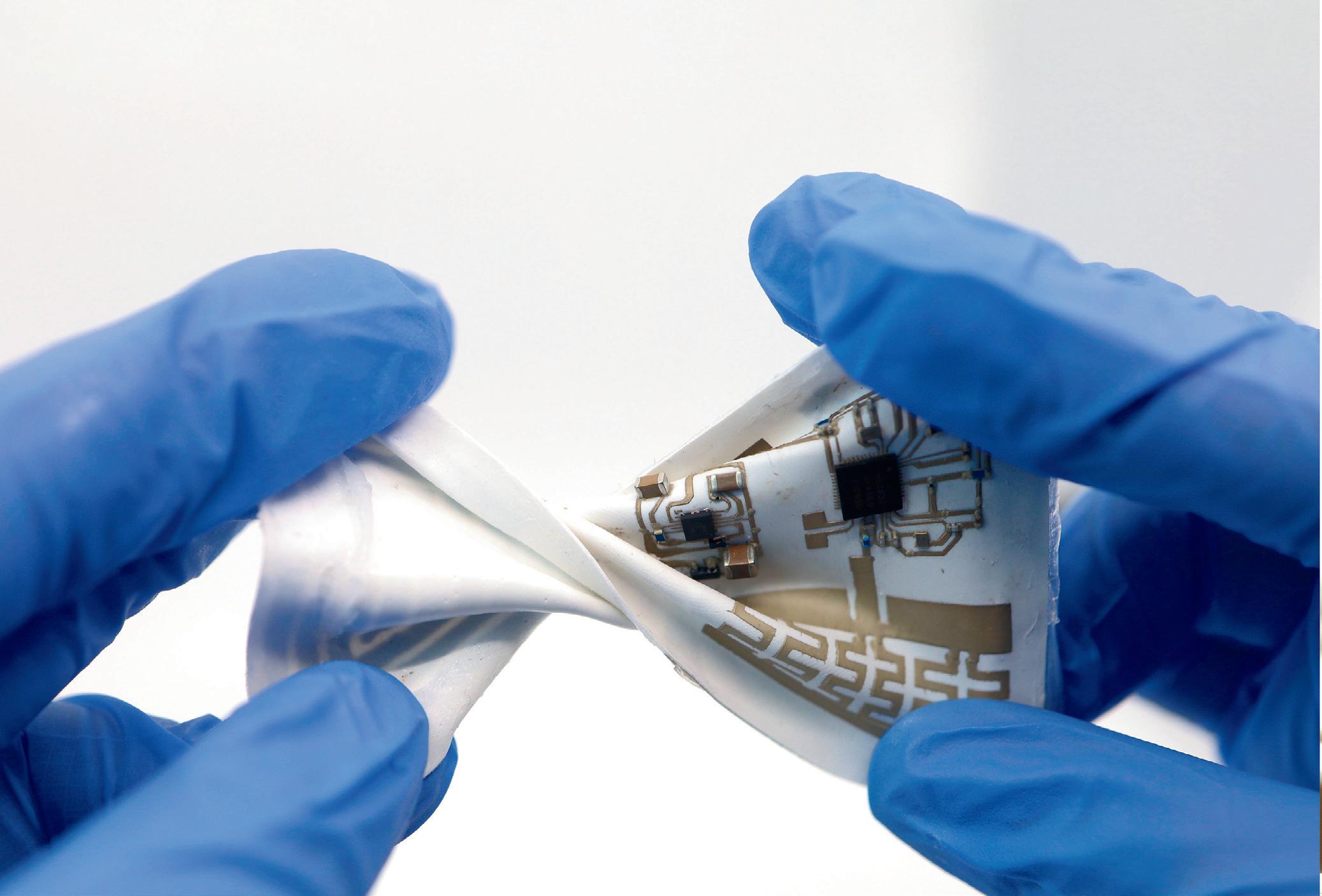
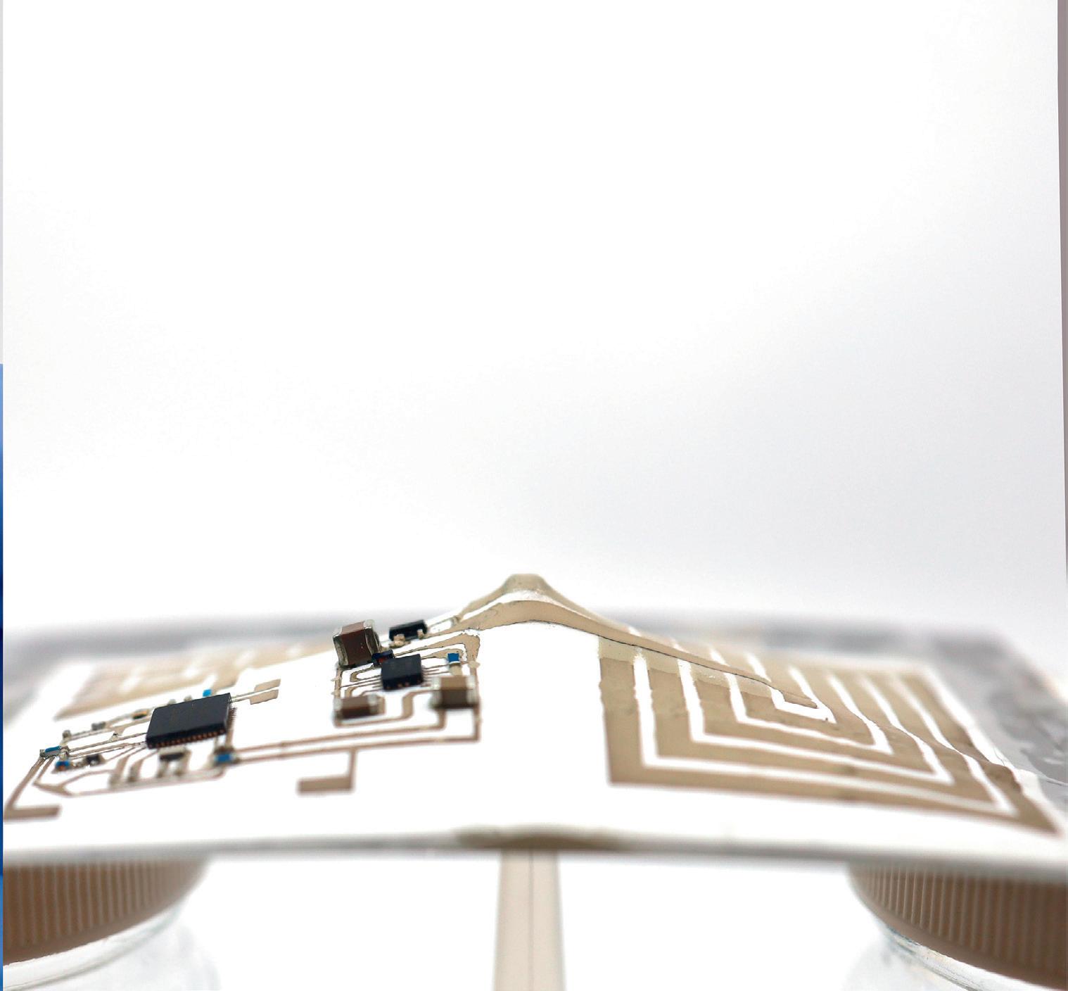
A new material that moves like skin while preserving signal strength in electronics could enable the development of next-generation wearable devices with continuous, consistent wireless and battery-free functionality.
According to a study published in Nature , an international team of researchers from Rice University and Hanyang University developed the material by embedding clusters of highly dielectric ceramic nanoparticles into an elastic polymer. The material was reverse-engineered to not only mimic skin elasticity and motion types, but also to adjust its dielectric properties to counter the disruptive effects of motion on interfacing electronics, minimise energy loss and dissipate heat.
“Our team was able to combine simulations and experiments to understand how to design a material that can seamlessly deform like skin and change the way electrical charges
distribute inside it when it is stretched so as to stabilise radiofrequency communication,” said Raudel Avila, assistant professor of mechanical engineering at Rice and a lead author on the study. “In a way, we are carefully engineering an electrical response to a mechanical event.”
Avila, who was responsible for conducting simulations to help identify the right choice of materials and design, explained that electronic devices use radiofrequency (RF) elements like antennas to send and receive electromagnetic waves.
“If you have ever been in a place with poor cellular reception or a very spotty Wi-Fi signal, you probably understand the frustra-
tion of weak signals,” Avila said. “When we’re trying to communicate information, we work at specific frequencies: two antennas communicating with each other do so at a given frequency. So we need to ensure that that frequency does not change so that communication remains stable. The challenge of achieving this in systems designed to be mobile and flexible is that any change or transformation in the shape of those RF components causes a frequency shift, which means you’ll experience signal disruption.”
The nanoparticles embedded in the substrate served to counteract these disruptions, with a key design element being the intentional pattern of their distribution. Both
Pictured are stretchable wearable devices incorporated on a newly developed material substrate that can adjust its dielectric properties to counter the disruptive effects of motion on interfacing electronics. The performance of the system was tested under various types of deforming motions, including twisting (left) and poking (right).
the distance between the particles and the shape of their clusters played a critical role in stabilising the electrical properties and resonant frequency of the RF components.
“The clustering strategy is very important, and it would take a lot longer to figure out how to go about it through experimental observations alone,” Avila said.
Sun Hong Kim, a former research associate from Hanyang and now a postdoctoral researcher at Northwestern University, pointed out that the research team took a creative approach to solving the problem of RF signal stability in stretchable electronics.
“Unlike previous studies that focused on electrode materials or design, we fo -
cused on the design of a high-dielectric nanocomposite for the substrate where the wireless device is located,” Kim said, highlighting the importance of collaboration across three different fields of expertise for developing “such a multidimensional solution to a complex problem”.
“We believe that our technology can be applied to various fields such as wearable medical devices, soft robotics and thin and light high-performance antennas,” said Abdul Basir, a former research associate from Hanyang and now a postdoctoral researcher at Tampere University in Finland.
Wearable technologies are having a profound impact on health care, enabling new
forms of individual monitoring, diagnosis and care. Smart wear market predictions reflect the transformative potential of these technologies with health and fitness owning the largest share in terms of end use.
“Wireless skin-integrated stretchable electronics play a key role in health emergencies, e-health care and assistive technologies,” Basir added.
To test whether the material could support the development of effective wearable technologies, the researchers built several stretchable wireless devices, including an antenna, a coil and a transmission line, and evaluated their performance both on the substrate they developed and on a standard elastomer without the added ceramic nanoparticles.
“When we put the electronics on the substrate and then we stretch or bend it, we see that the resonant frequency of our system remains stable,” Avila said. “We showed that our system supports stable wireless communication at a distance of up to 30 m (~98 feet) even under strain. With a standard substrate, the system completely loses connectivity.”
The wireless working distance of the far-field communication system exceeds that of any other similar skin-interfaced system. Moreover, the new material could be used to enhance wireless connectivity performance in a variety of wearable platforms designed to fit various body parts in a wide range of sizes.
For instance, the researchers developed wearable bionic bands to be worn on the head, knee, arm or wrist to monitor health data across the body, including electroencephalogram (EEG) and electromyogram (EMG) activity, knee motion and body temperature. The headband, which was shown could stretch up to 30% when worn on the head of a toddler and up to 50% on the head of an adult, successfully transmitted real-time EEG measurements at a wireless distance of 30 metres.
“Skin-interfaced stretchable RF devices that can seamlessly conform to skin morphology and monitor key physiological signals require critical design of the individual material layouts and the electronic components to yield mechanical and electrical properties and performance that do not disrupt a user’s experience,” Avila said. “As wearables continue to evolve and influence the way society interacts with technology, particularly in the context of medical technology, the design and development of highly efficient stretchable electronics become critical for stable wireless connectivity.”
Cross-sectional stereomicroscopic images of the dielectric polymer showing deformed (left) and undeformed (right) clusters. The cluster changes from sphere to ellipsoid under stretching deformations.
Raudel Avila/Rice University and Sun Hong Kim/Hanyang University.
Raudel Avila/Rice University and Sun Hong Kim/Hanyang University.
3D REFLECTORS HELP BOOST DATA RATE IN WIRELESS COMMUNICATIONS
David Nutt, Cornell Chronicle
The next generation of wireless communication not only requires greater bandwidth at higher frequencies — it also needs a little extra time.
Cornell researchers have developed a semiconductor chip that adds a necessary time delay so signals sent across multiple arrays can align at a single point in space, and without disintegrating. The approach will enable ever-smaller devices to operate at the higher frequencies needed for future 6G communication technology.
The team’s paper, ‘Ultra-Compact QuasiTrue-Time-Delay for Boosting Wireless Channel-Capacity’, was published in Nature The lead author is Bal Govind, a doctoral student in electrical and computer engineering.
The majority of current wireless communications, such as 5G phones, operate at frequencies below 6 gigahertz (GHz). Technology companies have been aiming to develop a new wave of 6G cellular communications that use frequencies above 20 GHz, where there is more available bandwidth, which means more data can flow and at a faster rate. 6G is expected to be 100 times faster than 5G.
However, since data loss through the environment is greater at higher frequencies, one crucial factor is how the data is relayed. Instead of relying on a single transmitter and a single receiver, most 5G and 6G technologies use a more energy-efficient method: a series of phased arrays of transmitters and receivers.
“Every frequency in the communication band goes through different time delays,” Govind said. “The problem we’re addressing is decades old — that of transmitting high-
bandwidth data in an economical manner so signals of all frequencies line up at the right place and time.”
This delay has previously been produced by phase-shifting circuits, but they can handle only so much data. That is a particular problem for wideband signals, in which the highest and the lowest frequencies can fall out of phase, causing the signal to blur, a phenomenon known as “beam squint”. And building time delays into a tiny chip that can fit in a smart phone is no small task.
“Most of the way that time delay is constructed is literally by using a long wire that will enable you to delay a signal from point A to point B. And we need that delay to be tuneable so that we can reroute this beam to different locations. We want it to be reconfigurable,” Apsel said.
Govind worked with postdoctoral researcher and co-author Thomas Tapen to design a complementary metal-oxidesemiconductor (CMOS) that could tune a time delay over an ultra-broad bandwidth of 14 GHz, with as high as 1 degree of phase resolution.
“Since the aim of our design was to pack as many of these delay elements as possible,” Govind said, “we imagined what it would be like to wind the path of the signal in three-dimensional waveguides and bounce signals off of them to cause delay, instead of laterally spreading wavelengthlong wires across the chip.”
The team engineered a series of these 3D reflectors strung together to form a “tuneable transmission line”.
The resulting integrated circuit occupies a 0.13 mm2 footprint that is smaller than phase shifters yet nearly doubles the channel capacity — ie, data rate — of conventional wireless arrays. And by boosting the projected data rate, the chip could provide faster service, getting more data to cellphone users.
“The big problem with phased arrays is this trade-off between trying to make these things small enough to put on a chip and maintain efficiency,” Apsel said. “The answer that most of the industry has landed on is, ‘Well, we can’t do time delay, so we’re going to do phase delay’. And that fundamentally limits how much information you can transmit and receive. They just sort of take that hit.
“I think one of our major innovations is really the question: Do you need to build it this way?” Apsel said. “If we can boost the channel capacity by a factor of 10 by changing one component that is a pretty interesting game changer for communications.”
The computer chip designed by Bal Govind and team.
Ryan Young/Cornell University.
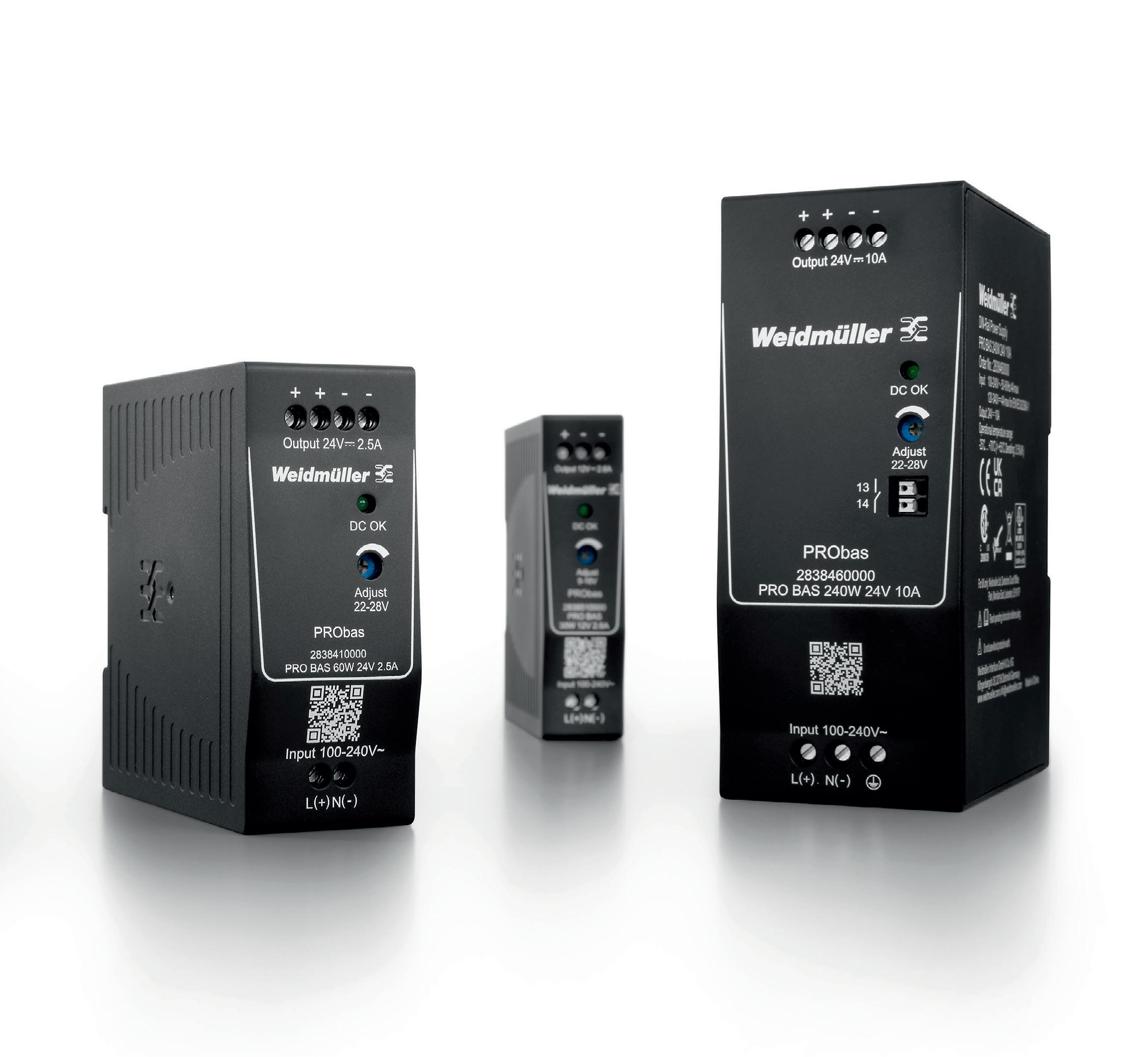
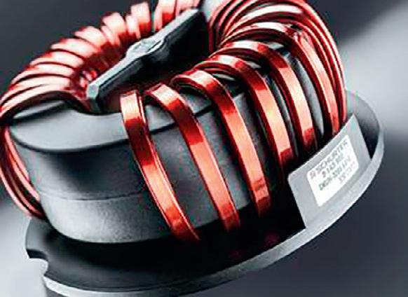
HIGH-CURRENT CHOKES
SCHURTER has launched a family of chokes for energy applications with particularly high power on the PCB. The DKUH-1 current- compensated chokes are designed for currents of up to 100 A and a rated voltage of up to 800 VDC.
The series of chokes features a compact and high-intensity design, combined with optimised energy efficiency. This leads to an increase in electromagnetic interference in modern electronic devices. This requires correspondingly powerful filter elements.
The bifilar winding and nanocrystalline cores in the DKUH-1 chokes facilitate high currents with compact dimensions. The chokes can be mounted directly on the PCB and soldered in a wave bath. The open design enables optimum cooling, both passive and active. This makes the members of the DKUH-1 family suitable for high power ratings in the energy range with voltages of up to 800 VDC.
The high-current chokes are suitable for energy applications such as EV fast-charging stations, battery storage, photovoltaics or energy converters. However, the new chokes are also designed for many high-power industrial applications. Inquiries for customised versions are welcome.
SCHURTER (S) PTE LTD www.schurter.com
COMPUTING SYSTEM
Backplane Systems Technology has launched the iBase AMI242 Intelligent System, a powerful, expandable fanless and ventless system designed to meet the demands of modern computing environments. This system is built around the iBase MBE240 proprietary board and supports 14th and 13th Gen Intel Core i9, i7, i5 and i3 desktop processors with a 35 W TDP, providing enhanced performance for a variety of applications.
A key feature of the system is its support for DDR5-5600 memory, with a maximum capacity of 64 GB, and optional ECC. The system is equipped with advanced networking capabilities, including two Intel 2.5G LAN ports and two Intel GbE ports that support 802.3 at PoE++, facilitating high-speed and versatile connectivity.
The system also offers extensive expansion options with three M.2 sockets (M-Key, B-Key, E-Key) and a PCI Express Generation 5 slot for 1x PCI-E (16x) expansion. This makes it adaptable to various peripheral requirements. Additionally, the system features dual SIM slots for WWAN redundancy, iAMT (16.1) for remote management and dTPM (2.0) for enhanced security.
Storage options include two 2.5 ″ slots supporting RAID 0/1 configurations, providing both performance and data redundancy. The system also includes protections against over, under and reverse voltage, enabling operation in challenging conditions.
Suitable for industrial and commercial applications, the iBase AMI242 offers a robust, fanless solution for high-performance computing needs. Backplane Systems Technology Pty Ltd www.backplane.com.au
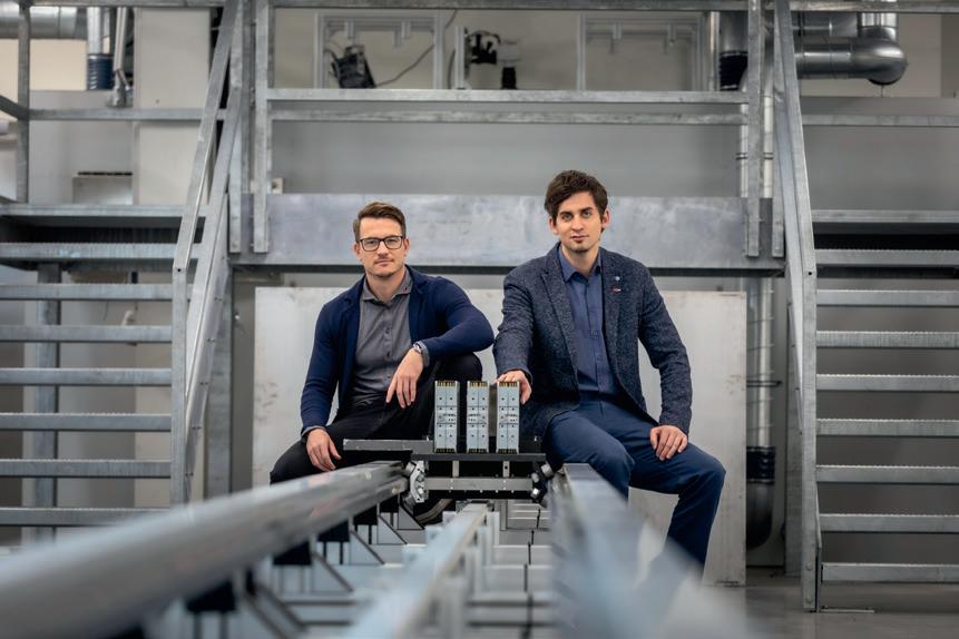
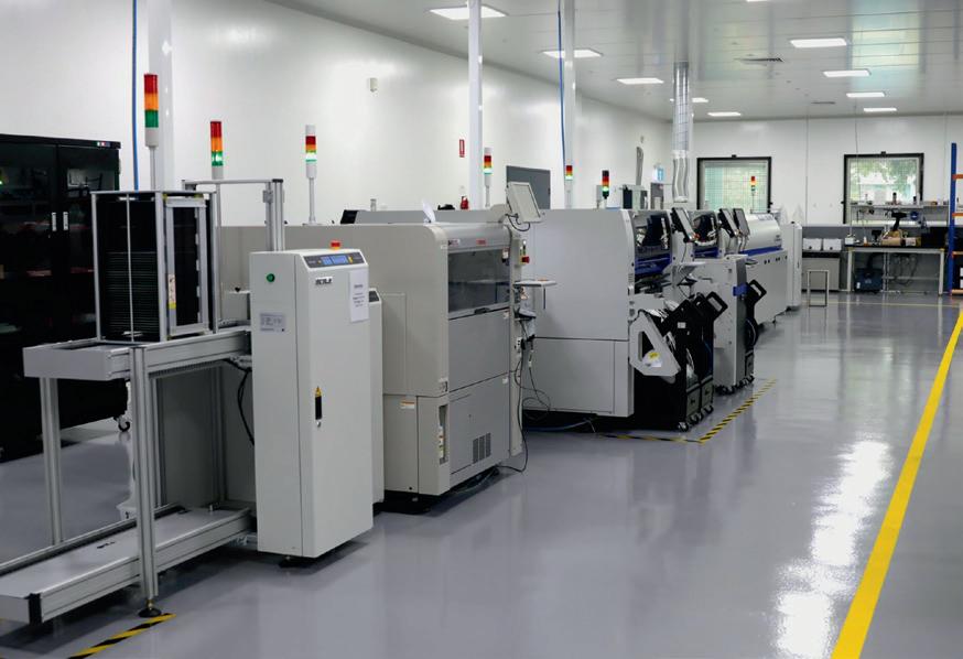
Enhancing Advatek Lighting’s business operations with a Hawker Richardson total line solution
Advatek Lighting was founded in Melbourne, Australia, in 2012 and quickly established a reputation within the professional lighting industry for its feature-rich, reliable, robust and flexible LED pixel control products. In 2021, the business consolidated its reputation for innovation and technical leadership with the launch of the PIXLITE MK3 RANGE, representing a quantum leap in LED pixel control capability.
Today, 90% of production ships to global markets from Advatek’s Australian production base, with more than 40,000 LED pixel control units exported to nearly 70 countries in the past decade.
Advatek PixLite controllers provide the technology behind many of the world’s most impressive lighting displays, ranging from public art installations to theme parks, night clubs and architectural applications. Examples have included Eurovision, the Burning Man Festival and the giant Dior Carousel of Dreams display on the Saks Fifth Avenue facade.
What factors played a pivotal role in the decision to opt for a total line solution
from Hawker Richardson?
The project covers the purchase, installation and commissioning of a state-of-the-art SMT line for assembly of specialised printed circuit board assemblies used in Advatek’s PixLite range of LED pixel control products.
The investment in this equipment from Hawker Richardson follows the construction of a temperature-controlled manufacturing environment from beginning to end, enabling Advatek to increase yield and customer satisfaction through improved quality and process control.
As we sought to understand and benchmark requirements to ensure the success of our investment, Advatek management called upon a range of specialists in areas such as manufacturing, ESD control, coatings, and so on.
Hawker Richardson proved themselves to be knowledgeable, reliable, and responsive in giving us the advice we needed to ensure the equipment specified would be fit for purpose now and into the future. We felt confident that Hawker Richardson would be best positioned to help us integrate the equipment into our business and systems, and provide a high level of ongoing care.
The acquisition of two YRM20s — was this a strategic move to achieve specific business objectives?
The investment in state-of-the-art Yamaha equipment represents a step change for Advatek Lighting, addressing the most complex and critical physical component of our products, giving the company greater control over quality and a raft of competitive benefits. As a growing, 100% Australian-owned business, Advatek Lighting has become a global player and an industry leader in pixel control through customer focus, world-leading technology and a recognised, high-quality product offering.
The acquisition of two YRM20s was specifically about ensuring that our production environment remains current well into the future and will be able to meet the needs of future product lines as the company continues to grow.
Due to the total line solution, do you anticipate a noticeable increase in product output?
Investment in the total line solutions will significantly enhance Advatek’s competitiveness and productivity by reducing manufacturing lead times and costs, increasing quality and reliability, decreasing time-to-market for new projects, lowering minimum manufacturing run volumes and reducing capital tied up in inventory.
By securing our future through increased productivity and competitiveness, this investment will improve job security for our valued employees. Advatek is a ‘born global’ business, already generating over 90% of revenue from export markets. Being relatively small and nimble, it is vital for the company to continue to reinvest in both R&D and manufacturing capability to remain in a leadership position in this highly competitive global industry.
Could you share your overall experience with Hawker Richardson’s service and support?
This was our first interaction with Hawker Richardson, and whenever you engage a new vendor with a project of this scale, there are naturally some uncertainties. We do try to thoroughly research in advance. With Hawker Richardson, we found that we were assigned a dedicated contact person and we were provided with a detailed timeline outlining each step of the process. This allowed us to know exactly what to expect and when, including shipping lead times for the equipment — a significant risk factor since port arrivals can’t always be guaranteed. We were quite pleased when Hawker Richardson proactively informed us of a slight delay, which they had already accounted for in their plan as a precaution.
As a result, everything proceeded almost exactly as planned. We had two or three technicians onsite who handled the laser levelling, installation, calibration, commissioning, assisted us in running some parts through and trained our staff. The experience and professionalism of the Hawker Richardson team were outstanding, and I rate it very highly. They guided us through each step carefully, ensuring there were no surprises. Therefore, I would absolutely recommend considering Hawker Richardson as a vendor for significant investments like this.
Hawker Richardson www.hawkerrichardson.com.au
THERMAL ANALYSIS SOFTWARE
Siemens Digital Industries Software has introduced Calibre 3DThermal, innovative software for thermal analysis, verification and debugging in 3D integrated circuits (3D-ICs). Calibre 3DThermal enables chip designers to model, visualise and mitigate thermal effects in their designs from early-stage chip and package-inward exploration through to design signoff by incorporating elements of Siemens’ Calibre verification software and Calibre 3DSTACK software along with the company’s Simcenter Flotherm software solver engine. Calibre 3DThermal provides the outputs necessary for thermal impacts to be considered in electrical simulations. Moreover, the software can both consume as input boundary conditions as well as provide output to Simcenter Flotherm — enabling true IC to system thermal modelling from IC to package to board to system level.
The software was developed to address challenges of 3D-IC architectures where controlling heat dissipation is a key requirement. It offers fast and comprehensive approaches to identifying and addressing complex thermal issues. The software also provides the flexibility to start initial feasibility analysis with minimal inputs and can later perform more detailed analyses considering metallisation details and their impact on thermal considerations as more detailed information becomes available. This enables designers to refine their analysis and apply fixes such as floor-planning changes and adding stacked vias or TSVs to avoid thermal hotspots and/or dissipate heat more effectively. This iterative process continues until the final assembly is complete, thereby reducing the risk of performance, reliability and manufacturing issues at final tape-out.
Like all Calibre products, Calibre 3DThermal is designed to integrate with a range of design tools from both third parties, as well as with Siemens’ software including the newly announced Innovator3D IC software. In all design flows, Calibre 3DThermal captures and analyses thermal data across the entire design lifecycle.
Siemens Ltd www.siemens.com.au
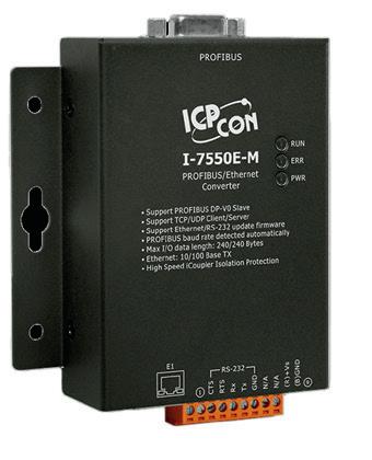
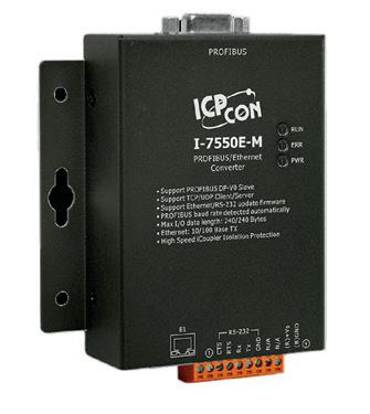
PROFIBUS TO ETHERNET CONVERTER
ICP Electronics Australia has launched the ICP DAS I-7550E-M PROFIBUS to Ethernet Converter, a robust and versatile device tailored for the PROFIBUS DP protocol’s slave devices. This converter facilitates communication between PROFIBUS masters and Ethernet devices that support TCP/UDP protocols. With automatic transmission rate detection and a configurable address range of 0 to 126, the I-7550E-M is designed to provide ease of integration and flexibility.
The device supports a maximum input and output data length of 240 bytes, accommodating a range of data transfer needs. Its configuration is straightforward via a web interface, allowing users to manage settings through any web browser. The device can also function as both a TCP/UDP server and client, providing adaptability to various networking requirements. Enhanced with high-speed iCoupler technology, the device features 2500 Vrms network isolation protection and 3000 VDC isolation on the PROFIBUS side, to enable performance in industrial environments. It meets CE, UKCA, FCC, RoHS and WEEE standards, underlining its compliance with international safety and environmental regulations.
Suitable for industrial, factory and process automation, the I-7550E-M simplifies integrating Ethernet devices into PROFIBUS networks, making it a valuable tool for modern automation systems. By bridging these two protocols, the I-7550E-M enhances communication and operational efficiency in various automated environments.
ICP Electronics Australia Pty Ltd www.icp-australia.com.au
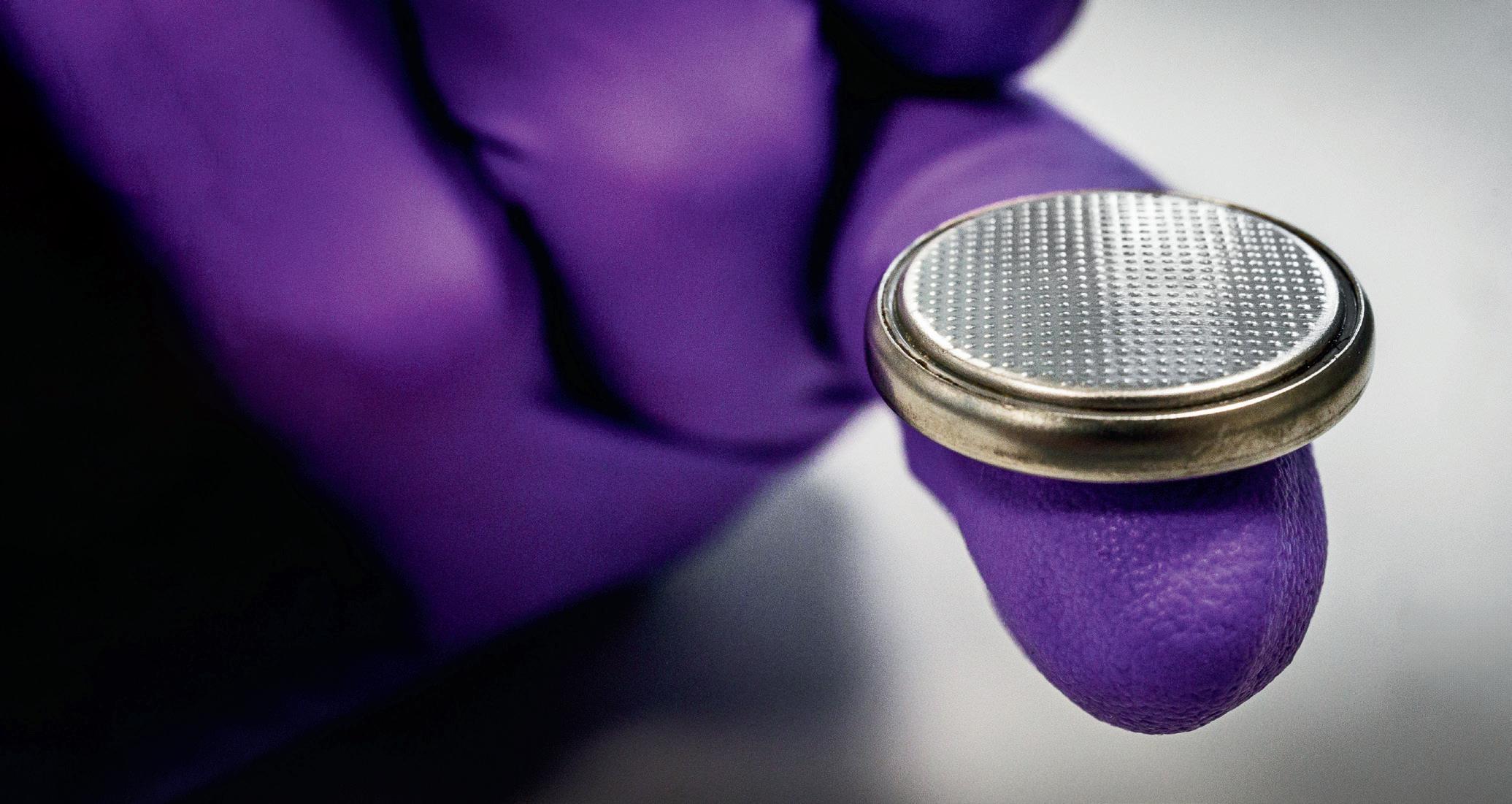
ECO-FRIENDLY BATTERY FOR LOW-INCOME COUNTRIES
Anders Törneholm, Linköping University
Researchers from Linköping University have developed a battery made from zinc and lignin that can be used over 8000 times.
The researchers aim to provide a cheap and sustainable battery solution for countries where access to electricity is limited. The study has been published in the journal Energy & Environmental Materials
"Solar panels have become relatively inexpensive, and many people in low-income countries have adopted them. However, near the equator, the sun sets at around 6 pm, leaving households and businesses without electricity. The hope is that this battery technology, even with lower performance than the expensive Li-ion batteries, will eventually offer a solution for these situations,” said Reverant Crispin, professor of organic electronics at Linköping University.
His research group at the Laboratory of Organic Electronics, together with researchers at Karlstad University and Chalmers, has developed a battery that is based on zinc and lignin, two cost-effective and environmentally friendly materials. In terms of energy density, it is comparable to lead-acid batteries, but without the lead, which is toxic.
Stable battery
The battery is stable, as it can be used over 8000 cycles while maintaining about 80% of its performance. Additionally, the battery retains its charge for approximately one week, significantly longer than other similar zinc-based batteries that discharge in just a few hours.
Although zinc-based batteries are already on the market, primarily as non-rechargeable batteries, they are predicted to complement and, in some cases, replace lithium-ion batteries in the long run when the feature of rechargeability is properly introduced.
“While lithium-ion batteries are useful when handled correctly, they can be explo-
sive, challenging to recycle, and problematic in terms of environmental and human rights issues when specific elements like cobalt are extracted. Therefore, our sustainable battery offers a promising alternative where energy density is not critical,” said Ziyauddin Khan, a researcher at the Laboratory of Organic Electronics at LiU.
Cheap and recyclable
The issue with zinc batteries has primarily been poor durability due to zinc reacting with the water in the battery’s electrolyte solution. This reaction leads to the generation of hydrogen gas and dendritic growth of the zinc, rendering the battery essentially unusable.
To stabilise the zinc, a substance called potassium polyacrylate based water-inpolymer salt electrolyte (WiPSE) is used. What the researchers at Linköping have now demonstrated is that when WiPSE is
used in a battery containing zinc and lignin, stability is very high.
“Both zinc and lignin are super cheap, and the battery is easily recyclable. And if you calculate the cost per usage cycle, it becomes an extremely cheap battery compared to lithium-ion batteries,” Khan said.
Scalable
Currently, the batteries developed in the lab are small. However, the researchers believe that they can create large batteries, roughly the size of a car battery, thanks to the abundance of both lignin and zinc at low cost. However, mass production would require the involvement of a company.
Crispin said that Sweden’s position as an innovative country enables it to assist other nations in adopting more sustainable alternatives.
“We can view it as our duty to help low-income countries avoid making the same mistakes we did. When they build their infrastructure, they need to start with green technology right away. If unsustainable technology is introduced, it will be used by billions of people, leading to a climate catastrophe,” Crispin said.
The research was primarily funded by the Knut and Alice Wallenberg Foundation through the Wallenberg Wood Science Centre, the Swedish Research Council, Åforsk, the Swedish Government’s strategic research area on advanced functional materials (AFM) at Linköping University, and Vinnova through Fun-Mat II. The long-term collaboration with Ligna Energy AB within the SESBC is funded by the Swedish Energy Agency.
This is a modified version of a news item published by Linköping University.
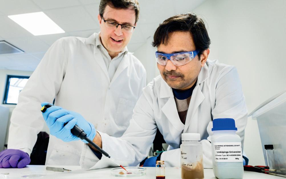
Reverant Crispin and Ziyauddin Khan, researchers at the Laboratory of Organic Electronics.
Thor Balkhed/Linköping University.
The battery developed by the researchers is small but the technology is scalable.
EDGE AI SERVERS
Designed for graphics-intensive workloads and on-premises AI training, the AIR-500 series of Edge AI servers from Advantech leverages up to four professional-grade NVIDIA RTX graphics cards, as well as Intel and AMD processors, thereby enabling data-driven computer vision and scientific AI applications in the industrial and medical fields.
The servers also offer up to 100 GbE Ethernet for mega-data processing, which is beneficial for healthcare applications such as examination data mining. This series includes the AIR-510, AIR-520 and AIR-530. Each features desktop- or server-grade CPUs and definable GPU configurations to fit diverse AI applications.
The AIR-510 and AIR-520 have completed NVIDIACertified Systems testing using the NVIDIA RTX A5000 and RTX 6000 Ada Generation GPUs, respectively. AIR-520 and AIR-510 also integrate the Phison aiDAPTIV+ solution for LLM fine-tune training on premises, reducing the barrier of adapting generative AI into enterprise settings and enhancing the security of sensitive data.
With Advantech and NVIDIA’s support services included with NVIDIA AI Enterprise, AI solution development can be accelerated to facilitate the efficient deployment of production-ready applications. Moreover, the AIR500 series complies with IEC-62368 safety standards and provides up to 10 years of longevity.
Advantech
Australia Pty Ltd www.advantech.net.au
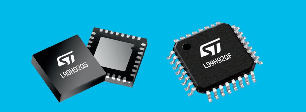
AUTOMOTIVE GATE DRIVER
The STMicroelectronics L99H92 automotive gate driver provides an SPI port for programming and diagnostics, a charge pump, protective features and two additional current-sense amplifiers for system monitoring.
Containing two high-side and two low-side drivers, the automotive gate driver can control a single H bridge powering one bidirectional DC motor or two half bridges for two unidirectional motors. Typical applications for the driver include electric sunroofs, window lifts, powered trunks, sliding doors and seatbelt pretensioners.
The charge pump powers the high-side drivers to maintain correct operation as the vehicle battery voltage fluctuates, enabling the outputs to function with a supply as low as 5.41 V. The charge-pump output is also available at an external pin to control a MOSFET for reverse-battery protection.
The gate-driving current is programmed through the SPI port, allowing slew-rate control to minimise electromagnetic emissions and thermal dissipation. Programming the current saves up to four external discrete components per MOSFET, typically needed for slew-rate setting with conventional drivers. The maximum drive current of 170 mA gives designers flexibility to use the driver with a variety of external MOSFETs, including high-power devices with large gate capacitance. With many features for system protection and diagnostics, the automotive gate driver is built for safety. There is overcurrent protection with a programmable threshold, detected by monitoring the MOSFET drain current. The device also features cross-conduction protection with a programmable dead time for safety and efficiency. Additional protection includes over-temperature early warning and shutdown, overvoltage and undervoltage protection on analog and digital power supply inputs, and open-load and output shortcircuit detection in off-state diagnostic mode.
A fail-safe input can turn off all MOSFETs instantaneously and a dedicated diagnostic pin provides immediate fault warning without waiting for periodic SPI transfers. Two current-sense amplifiers are also integrated for system-status monitoring. Suitable for high-side, low-side and inline sensing, the amplifiers have independently programmable gain, low offset and low thermal drift. They can be independently disabled to reduce current consumption when unused.
The L99H92 is in production now and packaged as a TQFP32 or QFN32 with wettable flanks to facilitate inspection.
STMicroelectronics Pty Ltd www.st.com
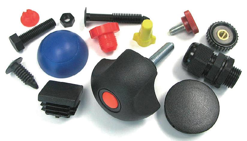
• Nylon Fasteners
• Screws & Nuts
• Washers & Spacers
• Rivets & Clips
• PCB Hardware
• Caps & Plugs
• Knobs & Handles
• Hole Pugs & Bushes
• LED Mounts & Light Pipes
• Cable Ties & Mounts
MINIATURISING A LASER ON A PHOTONIC CHIP
Lasers have revolutionised the world since the 60s and are now indispensable in modern applications, from cutting-edge surgery and precise manufacturing to data transmission across optical fibres.
But as the need for laser-based applications grows, so do challenges. For example, there is a growing market for fibre lasers, which are currently used in industrial cutting, welding and marking applications.
Fibre lasers use an optical fibre doped with rare-earth elements (erbium, ytterbium and neodymium, among others) as their optical gain source (the part that produces the laser’s light). They emit high-quality beams, they have high power output, and they are efficient, low-maintenance, durable and typically smaller than gas lasers. Fibre lasers are also the ‘gold standard’ for low phase noise, meaning that their beams remain stable over time.
But despite all that, there is a growing demand for miniaturising fibre lasers on a chip-scale level. Erbium-based fibre lasers are especially interesting, as they meet all the requirements for maintaining a laser’s high coherence and stability. But miniaturising them has been met by challenges in maintaining their performance at small scales.
Now, scientists led by Dr Yang Liu and Professor Tobias Kippenberg at EPFL have built the first ever chip-integrated erbiumdoped waveguide laser that approaches the performance with fibre-based lasers, combining wide wavelength tunability with the practicality of chip-scale photonic integration. The research findings have been published in Nature Photonics
Building a chip-scale laser
The researchers developed their chip-scale erbium laser using a state-of-the-art fabrication process. They began by constructing a metre-long, on-chip optical cavity (a set of mirrors that provide optical feedback) based on an ultralow-loss silicon nitride photonic integrated circuit.
“We were able to design the laser cavity to be metre-scale in length despite the compact
chip size, thanks to the integration of these microring resonators that effectively extend the optical path without physically enlarging the device,” Liu said.
The team then implanted the circuit with high-concentration erbium ions to selectively create the active gain medium necessary for lasing. Finally, they integrated the circuit with a III-V semiconductor pump laser to excite the erbium ions to enable them to emit light and produce the laser beam.
To refine the laser’s performance and achieve precise wavelength control, the researchers engineered an innovative intracavity design featuring microring-based Vernier filters, a type of optical filter that can select specific frequencies of light.
The filters allow for dynamic tuning of the laser’s wavelength over a broad range, making it versatile and usable in various applications. This design supports stable, single-mode lasing with a narrow intrinsic linewidth of just 50 Hz.
It also allows for significant side mode suppression — the laser’s ability to emit light at a single, consistent frequency while minimising the intensity of other frequencies (‘side modes’). This ensures ‘clean’ and stable output across the light spectrum for high-precision applications.
Power, precision, stability and low noise
The chip-scale erbium-based fibre laser features output power exceeding 10 mW and a side mode suppression ratio greater than 70
dB, outperforming many conventional systems.
It also has a very narrow linewidth, which means the light it emits is very pure and steady, which is important for coherent applications such as sensing, gyroscopes, LiDAR and optical frequency metrology.
The microring-based Vernier filter gives the laser broad wavelength tunability across 40 nm within the C- and L-bands (ranges of wavelengths used in telecommunications), surpassing legacy fibre lasers in both tuning and low spectral spurs metrics (“spurs” are unwanted frequencies), while remaining compatible with current semiconductor manufacturing processes.
Next-generation lasers
Miniaturising and integrating erbium fibre lasers into chip-scale devices can reduce their overall costs, making them accessible for portable and highly integrated systems across telecommunications, medical diagnostics and consumer electronics.
It can also scale down optical technologies in various other applications, such as LiDAR, microwave photonics, optical frequency synthesis, and free-space communications.
“The application areas of such a new class of erbium-doped integrated lasers are virtually unlimited,” Liu said.
The lab spin-off, EDWATEC SA, is an Integrated Device Manufacturer that can now offer Rare-Earth Ion-Doped Photonic Integrated Circuit-based Devices including high-performance amplifiers and lasers.
Optical image of a hybrid integrated erbium-doped photonic integrated circuit-based laser, providing fibre-laser coherence and previously unachievable frequency tunability.
Yang Liu (EPFL).
Nik Papageorgiou, EPFL
DEVICE GATHERS, STORES ELECTRICITY IN REMOTE SETTINGS
Brian Maffly, University of Utah
Today wirelessly connected devices are performing an expanding array of applications, such as monitoring the condition of engines and machinery and remote sensing in agricultural settings. Systems known as the Internet of Things (IoT), hold much potential for improving the efficiency and safety of the equipment.
Yet stumbling blocks remain for IoT, thwarting many potential applications. How do you power these devices in situations where and when reliable electrical sources are not practically available?
Research from the University of Utah’s College of Engineering points to a possible solution in the form of a novel type of battery called a pyroelectrochemical cell (PEC).
The device was developed and tested in the research labs of Roseanne Warren and Shad Roundy, both associate professors of mechanical engineering.
“It’s our idea for an integrated device that could harvest ambient thermal energy and convert it directly into stored electrochemical energy in the form of a supercapacitor or battery with applications for the Internet of Things and distributed sensors,” said Warren, the senior author on a new study that demonstrates a proof of concept.
“We’re talking very low levels of energy harvesting, but the ability to have sensors that can be distributed and not need to be recharged in the field is the main advantage,” she added. “We explored the basic physics of it and found that it could generate a charge with an increase in temperature or a decrease in temperature.”
The study is the cover feature in the 21 March edition of the journal Energy & Environmental Science , published by the Royal Society of Chemistry.
The device is charged by changing temperatures in the surrounding environment, whether it’s inside a car or aircraft or just under the soil in an agricultural environment. In theory, the PEC could power sensors for IoT applications that would otherwise be impractical to recharge.
A solar cell would work fine in some situations, according to Roundy, a co-author of the study.
“But in a lot of environments, you run into two problems,” Roundy said. “One is that it gets dirty over time. Solar cells have to be kept clean. So in these types of applications, they get dirty and their power degrades. And then there are a lot of applications where you just don’t have sunlight available. For example, we work on soil sensors that we put just under the top surface of the soil. You’re not going to get any sunlight.”
The PEC uses a pyroelectric composite material as the separator in an electrochemical cell. The material consists of porous polyvinylidene fluoride (PVDF) and barium titanate nanoparticles. This material’s electrical properties change as it’s heated or cooled, which decreases or increases the polarisation of the pyroelectric separator.
Changing temperatures create an electric field inside the cell, pushing ions around and enabling the cell store to energy.
“It stores electricity in what’s called an electric double layer, which stores the charge in positive and negative layers of ions. This is a glorified capacitor,” said lead author Tim Kowalchik, a graduate student in Warren’s lab. “When you heat and cool the system and you’re storing electrochemical energy, you’re changing the amount of positive or negative ions that are in those layers.”
The new study tested the lab’s theory of how the cell would operate.
“We had a predicted model of function that included what we called an ‘orientation effect’ in the paper,” Kowalchik said. “If we reverse the orientation of the separator in the
cell, it should drive ions the other way. This is a change we can make to the system that will show a different result that we can gather.”
The team’s experiments were set up to determine if the cells would respond as they predicted. Besides the orientation effect, there were heating vs cooling effects that needed to be tested.
“If you heat the thing one way, you should get something to happen. If you cool it first, you should get something to happen and that should show up differently,” Kowalchik said.
“We did that with a process called amperometry. You put a voltage across it and you hold that voltage constant and measure current. Your energy into the system is constant if nothing changes; if there is energy going into the system, the current changes.”
The cell did respond as the team theorised it would, but can it work outside a lab? That’s the next question Warren seeks to address. One of her students is now undertaking circuit modelling to design a cell and optimise its function.
“Now we start to change different parameters,” Warren said. “How can we improve the energy harvesting and storage and the combination of the two? And then after that would be a real-world field demonstration.”
The cell could produce up to 100 microjoules per square centimetre from a single heating/cooling cycle, which is not much energy, but enough to be useful for IoT purposes, according to the research.
“You want to monitor the condition of your car, the condition of machines, the condition of plants and soil and those kinds of things. Those types of sensors are generally going to be quite a bit lower power than your smartwatch or your phone, which have a display and they’re transmitting a lot of data,” Roundy said. “The sensors we’re talking about might just give periodic updates and they operate autonomously. They don’t have an interface or a screen.”
From left, Roseanne Warren, Shad Roundy and Tim Kowalchik pictured in Warren’s lab with a pyroelectrochemical (PEC) cell.
A pyroelectrochemical (PEC) cell is a device that converts thermal energy into electricity and stores it.
Brian Maffly.
Brian Maffly.
A Columbia Engineering team has published a paper in the journal Joule that details how nuclear magnetic resonance spectroscopy techniques can be leveraged to design the anode surface in lithium metal batteries.
The researchers also present new data and interpretations for how this method can be used to gain unique insight into the structure of these surfaces to share with the field.
“We believe that, armed with all the data we’ve pulled together, we can help accelerate the design of lithium metal batteries and help make them safe for consumers, which folks have been trying to do for more than four decades,” said the team’s leader Lauren Marbella, associate professor of chemical engineering.
The promise of lithium metal batteries
Batteries that use a lithium metal anode instead of a graphite anode, like the ones used in our cell phones and electric vehicles, will enable more affordable and versatile electrified modes of transportation, including semi-trucks and small aircraft. For example, the price of electric vehicle batteries would decrease while simultaneously offering a longer range (from 400 to >600 km).
Why they’re hard to commercialise
But commercialising lithium metal batteries is still far off in the future. Lithium metal is one of the most reactive elements on the periodic table and readily develops a passivation layer that impacts the structure of the anode itself during normal battery use. This passivation layer is like the layer that develops when silverware or jewellery begins to tarnish, but because lithium is so reactive, the lithium metal anode in a battery will begin to ‘tarnish’ as soon as it touches the electrolyte.
The chemistry of the passivation layer impacts how lithium ions move during battery charging/discharging, ultimately impacting whether or not metal filaments that lead to poor battery performance grow inside of the system. Up to now, measuring the chemical composition of the passivation layer, known by the battery community as the solid electrolyte interphase (SEI), while simultaneously capturing information on how lithium ions located in that layer are moving around, has been next to impossible.
DESIGNING
SAFER, HIGHER-PERFORMANCE
LITHIUM BATTERIES
Holly Evarts, Columbia Engineering
“If we had this information, we could start to draw connections to specific SEI structures and properties that lead to high-performance batteries,” Marbella said.
Results from the new study
The Joule study distils recent research, much of which the Marbella group has led or
contributed to, to present a case to leverage nuclear magnetic resonance (NMR) spectroscopy methods to connect the structure of the passivation layer on lithium to its actual function in the battery.
NMR enables researchers to directly probe how fast lithium ions move at the interface between the lithium metal anode
Lithium-ions approaching the solid electrolyte interphase on a lithium metal anode.
NMR
ENABLES RESEARCHERS TO DIRECTLY PROBE HOW FAST LITHIUM IONS MOVE AT THE INTERFACE BETWEEN THE LITHIUM METAL ANODE AND ITS PASSIVATION LAYER.
and its passivation layer, while also providing a readout of the chemical compounds that are present on that surface. While other characterisation methods, like electron microscopy, may provide striking images of the SEI layer on the surface of lithium metal, they cannot pinpoint the exact chemical composition of disordered species, nor can
they ‘see’ ion transport. Other techniques that can probe lithium transport across the interface, like electrochemical analyses, do not provide chemical information.
Examining the data collected in Marbella’s laboratory over the past six years, the team has found that NMR can uniquely sense changes in the structure of compounds in
the SEI on lithium metal, which is key to explaining some of its more elusive structureproperty relationships. The researchers believe that combining multiple techniques, like NMR, other spectroscopies, microscopy, computer simulations and electrochemical methods, will be necessary to advance the development of lithium metal batteries.
Applying NMR methods unveils new insights
When researchers expose lithium metal to different electrolytes, they often observe different performance metrics. Marbella’s NMR experiment shows that these changes in performance arise because different electrolyte compositions create distinct SEI compositions and deliver lithium ions to the anode surface at different rates. Specifically, when lithium metal battery performance improves, the rate of lithium exchange with the surface increases. They can now also see how the passivation layer should be arranged. To achieve the best performance, different chemical compounds must be layered on top of one another in the SEI, rather than randomly distributed.
The exchange experiments demonstrated in the new study can be used by materials scientists to help screen electrolyte formulations for high-performance lithium metal batteries as well as identify the surface compounds in the SEI that are required for high performance. Marbella added that NMR is one of the only techniques — if not the only — that can probe the local structural changes of compounds in the SEI to address how ionically insulating materials may enable fast lithium-ion transport in the SEI.
“Once we know what structural changes are occurring — for instance, are things like lithium fluoride becoming amorphous, defected, nano-sized — then we can intentionally engineer these in and design lithium metal batteries that meet the performance metrics required for commercialisation,” Marbella said. “The NMR experiment is one of the few that can accomplish this task and give us the very information essential to pushing anode surface design forward.”
Looking ahead
Marbella’s group is currently using exchange NMR coupled with electrochemistry to provide a deeper understanding of SEI composition and properties in different electrolytes for lithium metal batteries. They are also developing systems that can determine individual chemical components’ role in lithium-ion transport through the SEI.
AI CHIPS COULD GET A SENSE OF TIME
Katherine McAlpine, University of Michigan
Artificial neural networks may soon be able to process time-dependent information, such as audio and video data, more efficiently.
The first memristor with a ‘relaxation time’ that can be tuned has been reported in Nature Electronics , in a study led by the University of Michigan.
Memristors, electrical components that store information in their electrical resistance, could reduce AI’s energy needs by about a factor of 90 compared to today’s graphical processing units. Already, AI is projected to account for about 0.5% of the world’s total electricity consumption in 2027, and that has the potential to balloon as more companies sell and use AI tools.
“Right now, there’s a lot of interest in AI, but to process bigger and more interesting data, the approach is to increase the network size. That’s not very efficient,” said Wei Lu, the James R. Mellor Professor of Engineering at U-M and co-corresponding author of the study with John Heron, U-M associate professor of materials science and engineering.
The problem is that GPUs operate very differently from the artificial neural networks that run the AI algorithms — the whole network and all its interactions must be sequentially loaded from the external memory, which consumes both time and energy. In contrast, memristors offer energy savings because they mimic key aspects of the way that both artificial and biological neural networks function without external memory. To an extent, the memristor network can embody the artificial neural network.
“We anticipate that our brand-new material system could improve the energy efficiency of AI chips six times over the state-of-the-art material without varying time constants,” said Sieun Chae, a recent U-M PhD graduate in materials science and engineering, and co-firstauthor of the study with Sangmin Yoo, a recent U-M PhD graduate in electrical and computer engineering.
In a biological neural network, timekeeping is achieved through relaxation. Each neuron receives electrical signals and sends them on, but it isn’t a guarantee that a signal will move forward. Some threshold of incoming signals must be reached before the neuron will send its own, and it has to be met in a certain amount of time. If too much time passes, the neuron is said to relax as the electrical energy seeps out of it. Having neurons with different relaxation times in our neural networks helps us understand sequences of events.
Memristors operate a little differently. Rather than the total presence or absence of a signal, what changes is how much of the electrical signal gets through. Exposure to a signal reduces the resistance of the memristor, allowing more of the next signal to pass. In memristors, relaxation means that the resistance rises again over time.
While Lu’s group had explored building relaxation time into memristors in the past, it was not something that could be systematically controlled. But now, Lu and Heron’s team have shown that variations on a base material can provide different relaxation times, enabling memristor networks to mimic this timekeeping mechanism.
The team built the materials on the superconductor YBCO, made of yttrium, barium, carbon and oxygen. It has no electrical resistance at temperatures below -292°F (180°C), but they wanted it for its crystal structure. It guided the organisation of the magnesium, cobalt, nickel, copper and zinc oxides in the memristor material.
Heron calls this type of entropy-stabilised oxide the “kitchen sink of the atomic world” — the more elements they add, the more stable it becomes. By changing the ratios of these oxides, the team achieved time constants ranging from 159 to 278 nanoseconds, or trillionths
The entropy-stabilised oxide is sandwiched between the superconductor YBCO, on which it was grown, and a titanium and platinum electrode. The many colours represent the different components of the entropy-stabilised oxide. By tweaking the ratios of the components, the team could create memristors that relaxed at different rates after exposure to an electrical current, mimicking the way that neurons sense time.
of a second. The simple memristor network they built learned to recognise the sounds of the numbers zero to nine. Once trained, it could identify each number before the audio input was complete.
These memristors were made through an energy-intensive process because the team needed perfect crystals to precisely measure their properties, but they anticipate that a simpler process would work for mass manufacturing.
“So far, it’s a vision, but I think there are pathways to making these materials scalable and affordable,” Heron said. “These materials are earth-abundant, non-toxic, cheap and you can almost spray them on.”
The research was funded by the National Science Foundation. It was done in partnership with researchers at the University of Oklahoma, Cornell University and Pennsylvania State University. The device was built in the Lurie Nanofabrication Facility and studied at the Michigan Center for Materials Characterisation.
EMC_ad_2019.pdf 1 10/05/2023 10:32:41 AM
Bayswater
Sieun Chae and Sangmin Yoo, University of Michigan.
A ‘TED TALK’ IN THERMO DETECTION
The electronics industry faces a new challenge. While transistors in computer chips are shrinking, the heat they produce is only increasing. Overheating can cause reduced circuit performance, increased leakage power or even the total breakdown of transistors.
Ateam of researchers from the University of Pittsburgh and Carnegie Mellon University have proposed locally embedded thermoelectric devices (TEDs) that can perform active cooling inside circuits.
“Circuits like clock generators and arithmetic and logic units (ALU) create highfrequency heat fluxes with their peak hot spots occurring on the microprocessor,” explained Feng Xiong, associate professor of electrical and computer engineering at Pitt’s Swanson School of Engineering. “Cooling systems at the chip size are over-designed and a more targeted strategy is necessary to dissipate heat in these hot spots.”
TED Finds the hot spot
The only way to cool an object down is to remove the heat — or energy — from it. These circuits are generating heat at a really high frequency. With TED, this high frequency temperature variation can be totally eliminated.
TEDs remove heat from hot spots inside circuits to colder regions throughout the device using thermoelectric effects at the same frequency. Researchers proved their theory using experimental data from frequency domain thermal reflectance (FDTR) measurements made directly on an actively cooled thermoelectric device where the pump laser replicates the transient hot spot. The team used materials with high thermal conductivity, which theoretically improves cooling efficiency by a factor of 100 compared to conventional thermoelectric materials.
“We demonstrated a practical method to actively cancel the transient temperature variations on circuit elements with TEDs,” Feng said. “This result opens a new path to optimise the design of cooling systems for transient localised hot spots in integrated circuits.”
The paper, ‘Thermoelectric active cooling for transient hot spots in microprocessors’, was published in the journal Nature Communications
Westwick-Farrow Media
A.B.N. 22 152 305 336
www.wfmedia.com.au
Head Office Unit 5, 6-8 Byfield Street, North Ryde
Locked Bag 2226, North Ryde BC NSW 1670 Ph: +61 2 9168 2500