In 1965, Gordon E. Moore, a co-founder of Intel Corp., first proposed Moore’s Law, forecasting that the number of transistors on a silicon computer chip would double every two years. Originally expected to last a decade, Moore’s Law has been the guiding principle for advancements in semiconductor innovation for the last 60 years, symbolising the growth in computer capabilities and the demand for more advanced, compact technology applications. By shrinking transistor sizes and improving manufacturing techniques, semiconductor companies have been able to enhance computational power while reducing costs.
However, as we approach the physical limits of silicon-based semiconductor manufacturing, the industry has been pushed to explore new avenues of semiconductor manufacturing to sustain technological progress. This push for semiconductor innovation has prompted scientists to look beyond silicon-based electronics for new possibilities. This issue’s lead article, from Mouser Electronics, delves into the materials that have the potential to continue Moore’s Law, such as carbon-based semiconductors, compound semiconductors and photonic chips.
While electronic componentry is one of the key features of this issue, the magazine also includes an article on page 21 about a cryogenic CMOS chip, developed by researchers from the University of Sydney and the University of New South Wales. This issue also covers the development of an ultrasound diagnostic technique that identifies flaws in batteries, on page 26.
I welcome article submissions from our readers — so if you would like to offer any insights or expertise for future issues of the magazine, please do get in touch on the email address below.
As always, I hope you enjoy this issue.
Best wishes,
Ashna Mehta Editor
wnie@wfmedia.com.au
THE FUTURE OF THE SEMICONDUCTOR INDUSTRY
IN THE POST-MOORE ERA
Bell Labs established the information age in 1947 when they demonstrated the first transistor ever made using germanium semiconductors. The arrival of the silicon transistor seven years later marked the beginning of Moore’s Law, as it quickly emerged as the dominant material for integrated circuit (IC) technology.
According to Moore’s Law, the number of transistors that can be accommodated on an integrated circuit would double every year, extending this later to every 18 to 24 months. This translates to a doubling of microprocessor performance roughly every two years while simultaneously reducing chip costs. For over six decades, semiconductor development has followed Moore’s Law, contributing significantly to global economic growth, driving technological innovation, social transformation, productivity enhancements and economic expansion.
However, like most phenomena in the world, even the most remarkable eras even-
tually come to an end. While the future of Moore’s Law remains uncertain, with ongoing discussions about its slowing and eventual failure, the industry persists in developing methods to prolong its relevance.
From silicon-based to nonsilicon-based, does chip material have to change again?
For over half a century, silicon-based semiconductor technology, particularly complementary metal–oxide–semiconductor (CMOS) IC technology, has driven profound changes in human society. Nevertheless, it is now approaching both its physical and engineering limits. Since the early 21st century, the pace of silicon-based chip development has been gradually slowing, signalling the advent of the post-Moore era.
However, at the same time, the demand for data processing and storage capacity
continues to grow, prompting researchers and industry leaders to explore new materials and methods to extend and expand the principles behind Moore’s Law. This is driving scientists globally to search for viable alternatives to silicon.
Examining the materials that have the potential to continue Moore’s Law
Among the materials with the potential to sustain Moore’s Law, carbon-based semiconductors have received considerable attention due to their unique physical properties and extraordinary conductivity. Carbon nanotubes (CNTs) and graphene fall into this category and are considered as potential for future electronic, optoelectronic, and quantum devices.
Another notable alternative is compound semiconductors, which differ from elemental semiconductors such as silicon. These ma-
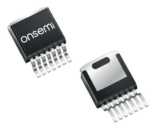
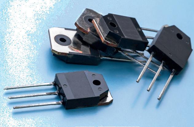
terials, composed of two or more elements, exhibit wide band gaps, high electron mobility and superior optoelectronic characteristics, making them well-suited for high-temperature, high-frequency, and optoelectronic applications. Notable examples include silicon carbide (SiC) (Figure 1), which have gained significant attention in recent years, as well as boron arsenide (BAs).
Additionally, organic semiconductor materials, which include conductive polymers and small-molecule organic semiconductors, are being used extensively in flexible electronics, optoelectronic devices and display technologies.
Other emerging materials are advancing notably in specific high-tech industries. Zinc oxide (ZnO) is increasingly valued for its role in creating transparent conductive oxides essential for Liquid crystal displays (LCDs) and photovoltaic solar cells, as well as serving as a photocatalyst for hydrogen production. Molybdenum disulfide (MoS 2)
is another material gaining attention for its potential in semiconductor applications, where its exceptional thin-layer properties and high electron mobility are advantageous. Meanwhile, due to its high charge capacity and favourable electrical properties, black phosphorus is being explored for light-emitting diodes (LEDs) and photodetectors.
Based on the current development, carbon nanotubes may be the direction with the greatest potential to continue Moore’s Law. Carbon-based semiconductors could offer reduced power consumption and higher efficiency, making them a strong candidate for the next generation of transistor-integrated circuits. However, it is difficult to produce materials that meet the requirements of carbon nanotubes. This is a problem that scientists have been working hard to solve. As early as 2009, carbon-based nanomaterials were included in the International Technology Roadmap for Semiconductors (ITRS) as a
future technology option, but at that time, the technology was too complicated to fabricate on a mass scale.
In recent years, key material challenges in semiconductor carbon nanotubes have been overcome, and the fabricated devices and circuits have demonstrated superior realworld electronic performance compared to silicon-based products. These breakthroughs bring the theoretical potential of carbonbased Integrated Circuits closer to reality and at a research level, demonstrate the potential competitive performance compared to conventional semiconductor technologies.
At the application level, carbon-based electronics show considerable potential in areas such as digital computing, radio-frequency electronics, sensing, 3D integrated circuits, specialised chips, display drivers and optoelectronic devices. Amongst these, carbon nanotube-based digital ICs (also known as carbon-based digital circuits) represent the most commercially and technically valuable avenue for carbon electronics. Recent advancements in this area mainly focuses on four aspects, including high-performance circuit exploration, low-power device innovation, complete digital logic function demonstration and large-scale integrated system research.
Quantum and light, a different approach?
Quantum and photonics technologies represent additional promising directions for the post-Moore era. Following decades of laboratory research and academic exploration, these fields are now approaching widespread commercial viability. In recent years, interest in using quantum and photonic chips to accelerate Artificial intelligence (AI) has
Mouser Electronics.
An onsemi M3S EliteSiC MOSFET, one of the SiC devices available from Mouser Electronics.
iStock.com/PonyWang
SINCE THE EARLY 21ST CENTURY, THE PACE OF SILICON-BASED CHIP DEVELOPMENT HAS BEEN GRADUALLY SLOWING, SIGNALLING THE ADVENT OF THE POST-MOORE ERA.
surged, driven by the fundamental need to enhance computational power while reducing energy consumption.
Photonic devices
Recent research highlights the potential of optical technologies to overcome the inherent limitations of electronic chip design. Photons travel faster than electrons and exhibit low power consumption, minimal latency and resistance to fluctuations in temperature, electromagnetic fields and noise. Consequently, photonic chips are widely regarded as a key technology that can surpass Moore’s Law.
Historically, fibre-optic technologies have been predominantly utilised in communication systems, taking advantage of light’s superior speed and bandwidth for long-distance data transmission. However, advancements in optical computing, including the development of embedded co-packaged silicon-photonic waveguides, are broadening the scope of applications to encompass fields such as AI, biosensing and light detection and ranging (lidar). By harnessing light instead of electrons, photonic devices can meet the increasing demand for speed across numerous applications while significantly reducing energy consumption. This paradigm shift could result in more efficient and potent computing systems, overcoming the limitations of traditional electronic architectures and unlocking new speed and energy efficiency.
Quantum computing
Quantum computing, on the other hand, utilises counterintuitive quantum mechanical properties to accelerate certain types of calculations. In principle, quantum computers possess exceptional parallel processing capabilities, enabling exponential speedups for tasks such as machine learning (ML), cryptographic decryption, big data optimisation, materials discovery and drug analysis.
Despite this potential, the commercialisation of quantum computing faces engineering and material challenges. Quantum bits (qubits), the fundamental units of quantum computation, are highly susceptible to environmental interference. To achieve practical quantum computing, researchers must develop robust error correction techniques.
Recent progress in quantum computing is driven by improvements in qubit quality, error rates, scalability and substantial investments from major technology firms and start-ups. Governments worldwide, including those of the United States, the United Kingdom, China and Germany, have collectively invested billions of dollars in quantum research, and leading technology companies such as Google, IBM, Microsoft and Intel are all actively advancing quantum computing from fundamental research to engineering realisation.
Quantum computing research follows three main technological paths, including superconducting, ion-trap and optical quantum computing. The superconducting approach
is the most competitive market; however, some researchers argue that optical quantum computing offers more potential.
Optical quantum chips utilise photons’ quantum properties for information processing and transmission. Light signals travel at 300,000 km/s through small circuits, and quantum properties such as superposition and entanglement enable computational capabilities that surpass those of classical computers. Achieving this requires integrating large numbers of photonic devices via lithographic techniques and precisely controlling them, but more fundamentally, manufacturing optical quantum computers entails a complete reinvention of chip mechanisms, fabrication processes and system integration.
Conclusion
The quest to surpass Moore’s Law is advancing on multiple fronts. Scientists are looking beyond silicon-based electronics for new possibilities. Whether it is through carbonbased electronics, quantum computing or photonic chips, these new technologies offer hope, but they also require extended periods of technological improvement.
In the era of traditional electronic chips, the world’s leading technology companies achieved prominence through decades of iterative development, large-scale industrialisation and application expansion, and the same will undoubtedly hold true for the next generation of semiconductor technologies.
BOOSTING NEAR-INFRARED HARVESTING IN TANDEM SOLAR CELLS
Researchers from the National University of Singapore have demonstrated a perovskite–organic tandem solar cell with a power conversion efficiency of 26.4% over a 1 cm2 active area, a development that reportedly makes it the highest-performing device of its kind to date. This milestone is driven by a newly designed narrow-bandgap organic absorber that enhances near-infrared (NIR) photon harvesting, a long-standing bottleneck in thin-film tandem solar cells.
This research breakthrough was achieved with guidance from Assistant Professor Hou Yi from the National University of Singapore. The research findings have been published in the scientific journal Nature
Perovskite and organic semiconductors both offer widely tuneable bandgaps, enabling tandem cells to approach high theoretical efficiencies. According to Hou, their light weight and flexible form factor makes perovskite–organic tandem solar cells suitable for power applications that are run directly on devices such as drones, wearable electronics, smart fabrics and other AI-enabled devices.
However, the absence of efficient NIT thin-film absorbers — which help to capture the sunlight in the NIR region more efficiently and therefore improve the overall efficiency of tandem cells — has kept perovskite–organic tandem cells lagging behind alternative designs.
To overcome this challenge, the researchers developed an asymmetric organic acceptor with an extended conjugation structure, enabling absorption deep into the NIR region while maintaining a sufficient driving force for efficient charge separation and promoting ordered molecular packing. Ultrafast spectroscopy and device physics analyses confirmed that this design achieves high free charge carrier collection with minimal energy loss.
Building on the organic subcell’s performance, the researchers stacked it beneath a high-efficiency perovskite top cell, interfacing the two layers with a transparent conducting oxide (TCO)-based interconnector. This tandem cell achieved a power conversion efficiency of 27.5% on 0.05 cm2 samples and 26.7% on 1 cm2 devices, with the 26.4% result independently certified. These findings reportedly mark the highest certified performance to date among perovskite-organic, perovskite-CIGS and single-junction perovskite cells at comparable size.
“With efficiencies poised to exceed 30%, these flexible films are ideal for roll-to-roll production and seamless integration onto curved or fabric substrates — think self-powered health patches that harvest sunlight to run onboard sensors, or smart textiles that monitor biometrics without the need for bulky batteries,” Hou said.
The researchers will now focus on enhancing real-world operational stability and advancing towards pilot-line manufacturing, to bring flexible, high-performance solar technology to market.
SEMICONDUCTOR ADVANCE PAVES THE WAY FOR FASTER ELECTRONICS
Researchers from Tohoku University, Cambridge University and the National Institutes for Quantum Science and Technology have demonstrated a new way to make a material known as tin sulfide (SnS), which can help build better and more compact electronic devices. The method can grow SnS in sheets so thin that they are comprised of one layer of atoms. This strategy could streamline the process of making SnS.
Makoto Kohda, a researcher from Tohoku University, said SnS is special because it can conduct electricity and respond to light in unique ways. “Our method makes it easier to study those unique properties, which are important because they could lead to faster, more efficient computers,” Kohda said.
Spin-valleytronics is an area of research that utilises both the “spin” and “valley” of tiny electron particles inside a computer with the aim of developing electronics with high efficiency. While SnS has many desirable traits, it is also challenging to selectively form SnS from base tin (Sn) and sulfur (S), as it may sometimes produce SnS2 instead. To ensure the material produced is correct, the researchers developed an easier and safer process that can reliably produce ensure sheets of SnS.
The researchers found that heating sulfur and tin in the right way can grow pure, high-quality SnS crystals
on ordinary silicon wafers. A computer-calculated phase diagram predicted that low sulfur levels should give SnS, while high sulfur levels should give SnS2. The researchers tested that prediction in the lab by sliding the sulfur source closer or father from the tin. Then, the researchers used operando scanning electron microscopy to watch the outer layers “sublime” away (going directly from a solid to a gas), leaving a monolayer film behind.
“Our findings could speed up how scientists discover and understand new physical effects using monolayer SnS,” Kohda said.
Linking together three research areas – ferroelectrics, spintronics and valleytronics – opens the door to creating better electronics, especially those that use light and tiny spins to work faster and smarter. The research findings have been published in the journal Nano Letters
The new perovskite–organic tandem cell (right) designed by NUS scientists can achieve a power conversion efficiency of 26.4%, outperforming the previous benchmark for similar devices.
National University of Singapore.
NEXT-GEN ADHESIVE TECHNOLOGY FOR MICRO-LED DISPLAYS
Researchers from Pohang University of Science and Technology (POSTECH) have developed a novel dry adhesive technology that allows everything from microscale electronic components to common household materials to be easily attached and detached. Micro-LEDs, a next-generation display technology, offer significant advantages such as higher brightness, longer lifespan and the ability to enable flexible and transparent displays. However, transferring micro-LED chips — thinner than a strand of hair — onto target substrates with high precision and minimal residue can be challenging.
Conventional methods that rely on liquid adhesives or specialised films often result in overly complex processes, poor alignment accuracy or residual contamination. Researchers have also struggled with the adhesion paradox — the theoretical prediction that surfaces should strongly adhere at the atomic level, contrasted by the real-world difficulty of achieving strong adhesion due to surface roughness that limits actual contact area.
The POSTECH researchers leveraged this paradox; their solution lies in the use of shape memory polymers (SMPs) featuring densely packed nanotips. At room temperature, the surface remains rough, exhibiting low adhesion. When heated and pressed, the surface smooths out and achieves stronger adhesion. Upon reheating, the surface returns to its original rough state, thereby reducing adhesion and enabling easy release.
This technology provides over 15 atmospheres of adhesion strength during bonding and near-zero force detachment through a self-release function. The difference in adhesion strength between the ‘on’ and ‘off’ states exceeds a factor of 1000. The researchers also demonstrated precise pick-and-place of micro-LED chips using a robotic system and confirmed stable adhesion even with materials such as paper and fabric.
“This innovation allows for the precise manipulation of delicate components without the need for sticky adhesives,” said Professor Seok Kim of POSTECH. “It holds significant potential for applications in display and semiconductor manufacturing, and could bring about transformative changes when integrated with smart manufacturing systems across various industries.”
The research findings have been published in the journal Nature Communications
ENHANCING EFFICIENCY OF TINBASED PEROVSKITE SOLAR CELLS
Perovskite solar cells are gaining attention as the next generation of solar technology due to their high efficiency, flexibility and potential for printing. Although lead-based perovskite has been used in high-efficiency solar cells, concerns regarding lead toxicity have led to interest in tin-based perovskite, which offers a more environmentally friendly alternative.
However, a challenge of tin-based perovskite solar cells is their lower energy conversion efficiency compared to their lead-based counterparts. The use of indene-C60 diadduct (ICBA), which consists of two indene molecules bonded to fullerene (C60), is known to enhance performance in the electron transport layer; however, the precise mechanism behind this improvement has yet to be fully understood.
Perovskite solar cells are structured with a perovskite crystal sandwiches between a hole transport layer and an electron transport layer; in this study, researchers from the University of Tsukuba used electron spin resonance to observe electron diffusion at the interface between the tin-based perovskite and the electron transport layer, while also examining band bending at this interface.
The investigation revealed that conventional PCBM, a fullerene derivative used in the electron transport layer, induces band bending at the interface with tin-based perovskite, facilitating charge recombination. This charge recombination leads to a reduction in open-circuit voltage (the maximum voltage available for extraction). By contrast, when ICBA is utilised in the electron transport layer, the researchers found that the resulting band bending effectively suppresses charge recombination, leading to higher opencircuit voltage.
The research findings are expected to enhance the efficiency of tin-based perovskite solar cells.
ADVANTECH INTRODUCES SYSTEMS PRE-CONFIGURED WITH IGNITION EDGE
Advantech Australia has announced an alliance with Inductive Automation to introduce a series of panel PCs and fanless embedded box PCs with Ignition Edge software pre-installed. This integration of industrial- grade hardware and software aims to provide complete, pre- configured solutions suitable for industrial applications, and is designed to minimise lead times and to accelerate and simplify deployment.
A line-up of six pre-configured
industrial-grade panel PCs (10.4 to 21.5″) and five box PCs (from palm-size to full-size) with varying configurations aim to provide flexibility and speed in choosing optimal systems suited for small to large Ignition projects. Engineered for industrial environments, the Advantech rugged solutions are designed for edge IIoT, HMI, small- to large-scale SCADA systems, MES systems and other missioncritical automation applications. On the software side, Ignition Edge is said to make digital transformation and edge computing easier and more affordable with unlimited tags and device connections and cross-platform compatibility.
The pre-configured systems are verified for compatibility and come pre-installed with Ignition Edge by Advantech CTOS, and configured locally in Australia, so that local users receive a ready-to-deploy unit, minimising testing and installation time. Ignition and Ignition Edge licences must be purchased separately to activate the software on Ignition Ready and Ignition Edge Ready systems.
Advantech said that Ignition Edge will also be available on all Advantech edge platforms depending on requirements.
BOOSTING DURABILITY OF ‘SMART WEARABLES’
Imagine a T-shirt that could monitor your heart rate or blood pressure. Or a pair of socks that could provide feedback on your running stride.
It may be closer than you think, with new research from Washington State University demonstrating a particular 3D ink printing method for so-called smart fabrics that continues to perform well after repeated washings and abrasion tests. The research, published in the journal ACS Omega, represents a breakthrough in smart fabric comfort and durability, as well as using a process that is more environmentally friendly.
Hang Liu, a textile researcher at WSU, said that the bulk of research in the field so far has focused on building technological functions into fabrics, without attention to the way fabrics might feel, fit and endure through regular use and maintenance, such as washing.
“The materials used, or the technology used, generally produce very rigid or stiff fabrics. If you are wearing a T-shirt with 3D printed material, for example, for sensing purposes, you want this shirt to fit snugly on your body, and be flexible and soft. If it is stiff, it will not be comfortable and the sensing performance will be compromised,” Liu said.
Initial methods of developing smart wearables involved gluing, weaving or sewing functional components such as conductive threads or sensors into fabrics. Newer approaches involving printing have shown promise, but have still faced problems with comfort and maintenance.
Liu’s team used direct ink writing 3D printing technology to print solutions of polybutylene succinate — a biodegradable polyester that is compatible with natural fibres — containing carbon nanotubes onto two types of fabric. The printed fabrics showed excellent electrical conductivity, mechanical strength, gauge factor and stability under repeated strains, and the solution’s ability to penetrate and bond with fibres gave the fabrics an enhanced washability and resistance to abrasion.
The researchers tested printed fabrics for tensile strength, electrical conductivity, their ability to function as motion sensors and other qualities. They found the fabrics continued to perform well after 20 cycles of washing and drying, and the surfaces did not scratch or crack after 200 cycles of abrasion testing or 500 cycles of tensile cyclic testing.
GALLIUM-DOPED TRANSISTORS BOOST COMPUTING POWER
Researchers from the Institute of Industrial Science, the University of Tokyo, have created a transistor from galliumdoped indium oxide (InGaOx). This material can be structured as a crystalline oxide, whose orderly, crystal lattice is suitable for electron mobility.
Transistors are integral components of modern electronics that amplify or switch electrical signals. As electronics become smaller, it is becoming increasingly difficult to continue scaling down silicon-based transistors. Now, the researchers from the University of Tokyo have developed a crystalline oxide transistor that features a ‘gate-all-around’ structure, whereby the gate, which turns the current on or off, surrounds the channel where the current flows.
“By wrapping the gate entirely around the channel, we can enhance efficiency and scalability compared with traditional gates,” said Anlan Chen, lead author of the study.
The researchers knew that they would need to introduce impurities to the indium oxide by ‘doping’ it with gallium. This would make the material react with electricity in a more favourable way. “Indium oxide contains oxygen-vacancy defects, which facilitate carrier scattering and thus lower device stability. We doped indium oxide with gallium to suppress oxygen vacancies and in turn improve transistor reliability,” said Masaharu Kobayashi, senior author.
The researchers used atomic-layer deposition to coat the channel region of a gate-all-around transistor with a thin film of InGaOx, one atomic layer at a time. After deposition, the film was heated to transform it into the crystalline structure needed for electron mobility. This process ultimately enabled the fabrication of a gate-all-around ‘metal oxide-based field-effect transistor’ (MOSFET).
“Our gate-all-around MOSFET, containing a gallium-doped indium oxide layer, achieves high mobility of 44.5 cm 2/Vs. Crucially, the device demonstrates promising reliability by operating stably under applied stress for nearly three hours. In fact, our MOSFET outperformed similar devices that have previously been reported,” Chen said.
The research findings have provided the field with a new transistor design that considers the importance of materials and structure, marking a step towards the development of reliable, highdensity electronic components suitable for applications with high computational demand, such as big data and artificial intelligence.
ELIMINATE UNPLANNED DOWNTIME
A SMARTER APPROACH TO MACHINE DIAGNOSTICS WITH THE HYDAC HMG 4000
Unplanned downtime is one of the biggest challenges in industrial operations, leading to costly disruptions, increased maintenance expenses, and lost productivity. Many maintenance teams struggle with outdated diagnostic methods that fail to detect early warning signs of equipment failure. Without accurate real-time data, predicting issues becomes difficult, often resulting in either unnecessary maintenance or catastrophic breakdowns. A proactive approach to machine health monitoring is the key to overcoming these challenges.
The Challenge: Inconsistent and Inefficient Diagnostics
Operators and technicians often face difficulties in assessing the true condition of their machinery. Relying on manual inspections or outdated monitoring tools can lead to:
• Undetected equipment failures due to limited measurement capabilities.
• Delayed maintenance, resulting in costly breakdowns.
• Time-consuming troubleshooting and inefficient repairs.
• Difficulty in capturing high-speed, dynamic processes. Without a reliable diagnostic tool, companies risk unplanned downtime, inefficiencies, and lost revenue.
The Solution: HYDAC HMG
4000 – Precision Data at Your Fingertips
The HYDAC HMG 4000 portable data recorder is designed to address these challenges by providing a smarter, faster,
and more precise approach to machine diagnostics and predictive maintenance. Key Features and Benefits:
• Comprehensive Data Acquisition: The HMG 4000 can simultaneously monitor up to 38 sensor inputs, including pressure, temperature, flow rate, and position, ensuring a complete view of your system’s health.
• High-Speed Measurement: With a sampling rate of up to 0.1 milliseconds, it captures rapid system changes, making it easier to detect transient faults and anomalies.
• User-Friendly Interface: Featuring a 5.7inch touchscreen, the intuitive design simplifies navigation and operation, allowing users of all skill levels to perform diagnostics with ease.
• Flexible Connectivity: Supports various input types, including IO-Link, CAN bus, and analogue signals, making it adaptable for different industrial applications.
• Real-Time Monitoring & Analysis: Enables event-driven measurements and records dynamic processes in real-time, helping maintenance teams make quick, informed decisions.
• Advanced Data Storage & Reporting: With the ability to store up to 500 measurements and approximately 8 million data points, long-term trend analysis and predictive maintenance planning become more efficient.
• Integrated Software for Enhanced Analysis: The included HMGWIN software allows for advanced visualisation,
reporting, and data archiving on a PC, facilitating deeper insights into machine performance trends.
Applications: Enhancing Maintenance Strategies Across Industries
The HYDAC HMG 4000 is an essential tool for:
• Predictive Maintenance: Prevent unexpected failures by detecting anomalies before they lead to major issues.
• Troubleshooting & Servicing: Quickly diagnose and resolve faults with detailed real-time analysis.
• Research & Development: Capture and analyse system behaviour during testing phases to optimise equipment performance.
• System Commissioning: Verify machine health and performance before deployment to reduce future risks.
Maximise Uptime and Efficiency with HYDAC HMG 4000
By equipping your maintenance team with the HYDAC HMG 4000, you gain a powerful tool for reducing downtime, optimising asset performance, and improving overall operational efficiency. Don’t wait for failures to disrupt your business—embrace smart diagnostics today and stay ahead of potential issues.
FUTURE ELECTRONICS
— DUE TO
BETTER ELECTRONICS PERFECT TIMING
Anna Ettlin, Empa
Our everyday lives are so riddled with electronics that we hardly notice them anymore. When we casually reach for our smartphone, we rarely think about how complex this device is. Hundreds of tiny components work together within it — each of them a high-precision masterpiece of engineering.
These rarely noticed components include radio frequency (RF) filters. They ensure that a device only receives the correct signals, whether via Wi-Fi or mobile networks. Every device that communicates wirelessly contains such filters. They are often based on piezoelectric thin films. Piezoelectric materials have a special feature: They generate electric charges when they are deformed and change shape in return when an electrical voltage is applied.
In addition to RF filters, piezoelectric thin films are used for many other components in microelectronics, whether as sensors, actuators or tiny energy converters. Additional applications, such as quantum technologies, are the subject of ongoing research. However, one thing is clear: For such thin films to do their job, they need to be of a very high quality. Depending on the composition and function of the thin film, this calls for different manufacturing processes.
Empa researchers from the Surface Science & Coating Technologies laboratory have developed a new deposition process for piezoelectric thin films. The novelty: Their method allows the high-tech layers to be produced in very high quality on insulating substrates and at relatively low temperature — a first in the field. The researchers have published their results in the journal Nature Communications and applied for a patent for the process.
New strengths for a well-known process
The researchers used a common technique called HiPIMS — short for high power impulse magnetron sputtering — as their starting point. Magnetron sputtering is a coating process in which material is deposited from a solid precursor material — the target — onto the component to be coated — the substrate. To achieve this, a process-gas plasma is ignited at the target. The process-gas ions — usually argon — are then shot at the target, knocking out atoms that subsequently land on the substrate to form the desired thin film. Many materials can be used as targets. For piezoelectric applications, metals are commonly used, often with the addition of nitrogen to produce nitrides such as aluminium nitride.
HiPIMS works in almost the same way — except that the process does not take place continuously, but in short, high-energy pulses. This not only means that the ejected target atoms travel faster — many of them are also ionized on their way through the plasma. This makes the process interesting for research. In contrast to neutral atoms, ions can be accelerated, for example by applying a negative voltage to the substrate. Over the past 20 years or so, this approach has been used to produce hard coatings, with the high energies resulting in especially dense and durable layers.
However, until now, this process was not viable for piezoelectric thin films. This is because applying a voltage to the substrate does not only accelerate the film-forming target ions, but also argon ions from the process gas. This argon bombardment must be avoided. “Several percent of argon can sometimes be incorporated in hard coatings,” said Empa researcher Sebastian Siol. ”Piezoelectric thin films often
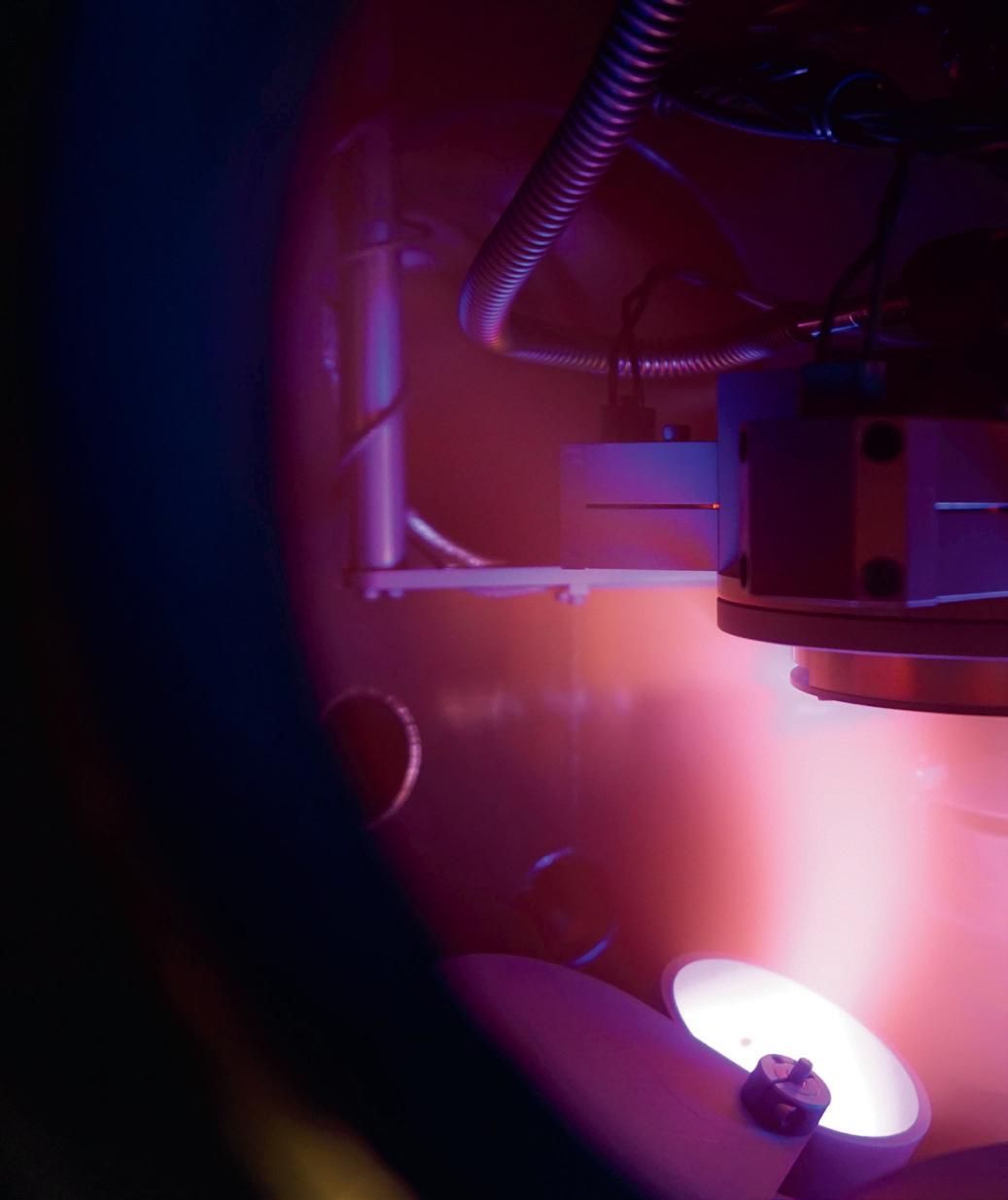
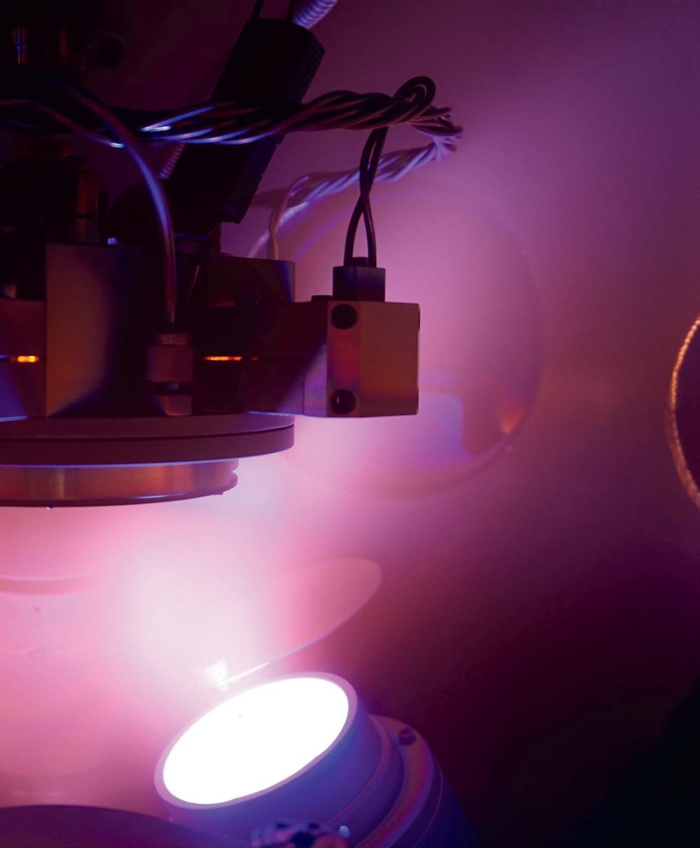
Argon plasma in the vacuum chamber during magnetron sputtering, with the substrate in the center of the photograph.
operate under high voltages. Here, such impurities could lead to a catastrophic electrical breakdown.”
Nevertheless, Siol’s team believed in the potential of HiPIMS for piezoelectric thin films. The high energy with which the ions fly towards the substrate is extremely advantageous. If the ion hits the substrate with sufficient energy, it remains mobile for a short time and can find an optimal position in the growing crystal lattice. But what can be done about the undesired argon inclusions?
During his doctoral thesis, Jyotish Patidar developed a clever solution. Not all ions arrive at the target at the same time. The majority of argon ions are located in the plasma in front of the target. This means that they often reach the substrate before the target ions, which first must be knocked out of the target and then have to cross the entire distance to the substrate. Patidar’s innovation was in the timing: “If we apply the voltage to the substrate at exactly the right moment, we only accelerate the desired ions,” Siol said. The argon ions have already flown past at this point — and without the additional acceleration, they have too little energy to be incorporated in the growing film.
‘Electron shower’ as a flight controller
Using this trick, the researchers were able to produce high-quality piezoelectric thin films with HiPIMS for the first time — with a performance equivalent to or even better compared to conventional methods. Now came the next challenge: Depending on the specific application, thin films need to be produced on insulating substrates, such as glass or sapphire. However, if the substrate is non-conductive, no voltage can be applied to it. Although there is a method in industry to accelerate the ions anyway, but this also often leads to argon inclusions in the layer.
This is where the Empa researchers achieved a breakthrough. To accelerate the ions onto the insulating substrate, they use the magnetron pulse itself — the short impulse that shoots the process gas ions onto the target. The plasma in the chamber contains not only ions, but also electrons. Each pulse from the magnetron automatically accelerates these negatively charged elemental particles onto the substrate. The tiny electrons reach the target much faster than the much larger ions.
Normally, this ‘electron shower’ is not relevant for the HiPIMS process. However, when the electrons arrive at the substrate, for a fraction of a second, they give it a negative charge — enough to accelerate the ions. If the researchers trigger a subsequent magnetron pulse at exactly the right time interval, the electron shower accelerates the target ions that started their flight during the previous pulse. And of course, the timing can also be adjusted so that only the right ions end up in the thin film.
From chips to qubits
The results are impressive: “With our method, we were able to produce piezoelectric thin films on insulating substrates just as well as on conductive ones,” Siol said. The researchers have termed the process Synchronized Floating Potential HiPIMS, or SFP-HiPIMS for short.
The big advantage: with SFP-HiPIMS, piezoelectric thin films can be produced in very high quality at low temperatures. This opens up new possibilities for the production of chips and electronic components, which often cannot withstand high temperatures. The technique for insulating substrates is particularly important for the semiconductor industry: “Many production tools in the semiconductor industry are designed in such a way that there is not even a possibility to apply an electrical voltage to the substrate,” Siol said.
In the next step, he aims to work on the development of ferroelectric thin films with his team — another key technology in current and future electronics. Based on this success, the Empa researchers are also launching several collaborations with other research institutions to bring their thin films into applications ranging from photonics to quantum technologies. And finally, they want to further optimise the innovative process with the help of machine learning and high-throughput experiments.
The team led by Empa researchers Jyotish Patidar and Sebastian Siol has enabled the production of high-quality piezoelectric thin films using the HiPIMS process through clever timing.
Empa.
Empa.
INDUSTRIAL MONITORS
ICP Electronics Australia has launched the iEi DM2 Series of industrial display solutions — a comprehensive line of touch monitors built to withstand demanding environments.
Designed for applications such as factory automation, transportation hubs, kiosks and more, the monitors blend robust engineering with modern aesthetics. With screen sizes ranging from 10.1 to 23.8 ″ , including square, widescreen and ultra-wide formats, the monitors can meet a range of installation needs.
Each monitor features a high-brightness display (up to 1000 nits) with anti-glare and anti-UV PCAP touchscreens, providing clear visibility in bright or outdoor environments. The front panel is also IP65-rated for protection against dust and water, and the entire unit supports a wide operating temperature range of -20 to 60°C.
Optional features such as a built-in 720p wide-angle, fixedfocus camera, dual 2W speakers and an integrated USB hub enhance user interaction and system integration. With multiple mounting options and front-accessible OSD buttons, installation and adjustments are made simple and accessible.
Whether upgrading an existing industrial HMI set-up or building a new interactive system from the ground up, the IEI DM2 Series offers a versatile, rugged and future-ready solution. ICP Electronics Australia www.icp-australia.com.au
ELECTRONIC SYSTEMS DESIGN SOFTWARE
ADVANTECH HMI TPC-100W SERIES PANEL PC
Advantech has announced that its Arm-based HMI TPC-100W series of Panel PCs, powered by NXP’s
i.MX 8M Mini quad-core processor, has achieved Arm SystemReady IR certification. The panel PCs now feature Secure Boot, a critical safeguard against unauthorised firmware and malicious code. Using Public Key Infrastructure (PKI), this security layer protects system integrity and safeguards sensitive operations from cyberthreats.
With SystemReady IR certification, the panel PCs adhere to industry standards, including support for UEFI (Unified Extensible Firmware Interface). UEFI enables consistent boot processes, reducing integration complexity and improving system compatibility — key for industrial applications where uptime is vital.
The certification also enables support for a wide range of operating systems, including Linux Yocto, Ubuntu and Debian. This compatibility helps ensure minimal customisation and facilitates integration into existing ecosystems. Standardised boot processes facilitate automatic security updates, helping developers focus on application development rather than system configuration.
With the TPC-100W series, Advantech empowers industrial clients to accelerate deployment, enhance cybersecurity and reduce time-to-market.
Advantech Australia Pty Ltd www.advantech.net.au
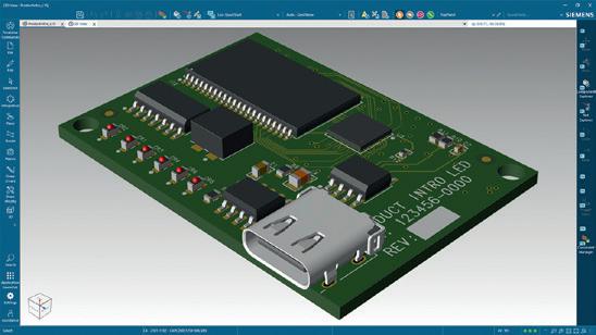
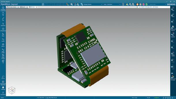
Siemens Digital Industries Software has launched the PADS Pro Essentials software, thereby making its AI-enhanced electronic systems design technology more accessible for small and medium-sized business.
Built on Siemens’ Xpedition technology, this new offering combines intuitive user experiences, integrated cloud collaboration and AI-driven automation.
The software is designed to deliver a streamlined, cloud-connected design environment built on Siemens’ Xpedition technology at an entry-level price. Tailored for independent engineers and start-ups, it includes schematic capture, layout and an enhanced design experience that lowers barriers to professional-grade PCB design tools. The Essentials tier also introduces an integrated, co-branded front-end powered by CELUS, allowing engineers to design using intelligent functional blocks with AI-assisted schematic and BOM generation.
Part of the Siemens Xcelerator portfolio of industry software, the new offering is part of the Xpedition family and is designed to grow with engineers, from individual users to global enterprises. The unified user experience, design libraries and cloudbased collaboration infrastructure provide a seamless upgrade path as team and project requirements evolve. Siemens Digital Industries Software www.siemens.com.sg/en
HVAC ENCLOSURES
OKW Gehäusesysteme offers a range of enclosures for heating, air conditioning and environmental applications. Even in their standard versions, the enclosures feature functional designs and protection classes up to IP67. Recessed operating areas to protect membrane keypads and displays, recessed surfaces to protect interfaces, high-quality materials and a range of accessories characterise these products and make them suitable for use in harsh environments.
Whether for mobile measuring instruments, permanently installed control units or IoT sensor systems, these enclosures are built for long-term use. Thanks to the variety of systems available, the enclosures are suitable for a range of applications in heating, air conditioning and environmental technology. Whether for control and monitoring devices for heating/air conditioning/ventilation systems, mobile data recording and transmission, smart devices for IoT-based environmental monitoring, or measuring and control devices in smart farming — there are countless applications that require technical enclosures and operating elements without compromising on functionality and design.
The tailored solutions also offer a range of customisation options. With services such as mechanical processing, printing, laser marking and much more, the result is a customer-specific product that is designed for the customer’s intended application.
ROLEC OKW Australia New Zealand P/L www.okw.com.au
MEMRISTOR-BASED HARDWARE TO ADVANCE AI
University of Massachusetts Amherst
Artificial intelligence (AI) is rapidly emerging as a force in nearly every sector of society. Yet the computer hardware in use today is based on hardware introduced over 75 years ago, relying on the transistor device first invented in 1947.
Thus far, computer engineers have largely kept up with the increased demands of advancing technology through various ‘brute force’ methods, such as decreasing device size and increasing bandwidth, explains Qiangfei Xia, the Dev and Linda Gupta Professor of Electrical and Computer Engineering at UMass Amherst. The result, though, is that AI programs are enormously expensive to run, both in terms of monetary cost — limiting access to major corporations and the super wealthy — and environmental impacts, including carbon emissions and freshwater use. For example, training a large language model that powers the popular chatbot ChatGPT could cost over $10 million and consume more than 700,000 litres of fresh water.
“AI is incredible. In 2016, we saw its potential when AlphaGo, an AI-based computer
system created by a Google subsidiary, beat the reigning human champion at the ancient Chinese board game Go,” Xia said. “But what most people don’t know is that the computers running AlphaGo filled nearly an entire room, and playing one game cost thousands of dollars in electricity.”
For the past decade, Xia and his collaborators have been developing a ‘memristor’ device to build new computers. They have demonstrated that this new analog computing device can complete complex computing tasks while bypassing the limitations of digital computing and using far less energy. And they believe that memristor technology holds the potential to advance AI and address many of today’s most pressing scientific questions, from nanoscale material modelling to large-scale climate science.
The Nanodevices and Integrated System Lab, headed by Xia, has been addressing
pressing issues in AI hardware and has a significant impact on emerging hardware based on transition metal oxide memristive devices. Xia has been recognised for his contributions to this field, as an elected Fellow of the Institute of Electrical and Electronics Engineers (IEEE).
The promise of memristive computing
According to Xia, the concept of memristor devices dates back to 1971, when it was first proposed by a professor at the University of California Berkeley. Work on the memristor remained mostly theoretical for decades, but in the late 2000s, HP — where Xia was working at the time — made a breakthrough by connecting the memristor concept to a physical device the company built in the lab. While transistors rely on the movement of electrons, the memristor takes inspiration from the human brain, in which ions move through hundreds of trillions of synapses to carry information. The memristor controls the flow of electrical current in a circuit, while also ‘remembering’ the prior state, even
when the power is turned off, unlike today’s transistor-based computer chips, which can only hold information while there is power. In the memristor, computing is performed at the site where data is stored, rather than moving data between the computer’s memory and processing modules.
Xia draws an analogy between this form of ‘in-memory computing’ and the empty roads during the early days of the COVID-19 pandemic. “Everyone was working from home, so that reduced traffic on the roads substantially.” For a computer built with memristive technology, these empty ‘roads’ mean a huge boost in energy efficiency and computing throughput. This opens many doors for creating low-power AI hardware, especially for edge computing, where data is processed in the devices that collect it, rather than being sent to a centralised cloud server. Potential applications include consumer electronics — such as lightweight AR/VR goggles or wireless earbuds — scientific research and military technology.
Xia and his collaborators see great potential for commercialising this technology.
In 2018, they founded TetraMem, a Silicon Valley-based startup of which Xia is a cofounder and advisor.
“We want to work together and transfer this technology to mainstream foundries so it can benefit users more broadly in the future. The memristor technology is now far enough along in development that this is an ideal time for industry to take over. In university research, we’ll continue finetuning the technology and exploring novel applications, such as in 6G cellular network technology and language processing, to name a few,” Xia said.
Computing inspired by the human brain
Going forward, Xia aspires to build computer circuits that are even more inspired by neuroscience and work as efficiently as the human brain. “We want to design a memristor device that’s a step closer to how our biological neurons work. This is known as neuromorphic computing,” Xia said.
Returning to the story of AlphaGo’s victory, Xia said the computer was estimated to use around 150 kilowatts of power to play the game, while its human competitor used only about 20–25 watts in its highly efficient brain. The human brain is also incredibly powerful in its capabilities. For example, we can recognise another person instantaneously based on only partial information, while digital computers must still do pixel-by-pixel matching.
“We have a long way to go. Literally, we do not understand our brains well enough yet. We want to use what we have already learned from the brain to build the next-generation computer. This will require collaboration with not just electrical engineers and computer scientists but also neuroscientists and psychologists. I feel so lucky to be working in this field during this time when AI is booming. I’m very hopeful for the next phase of truly brain-inspired computer hardware,” Xia said. This is a modified version of a news item published by the University of Massachusetts Amherst.
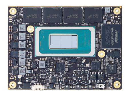
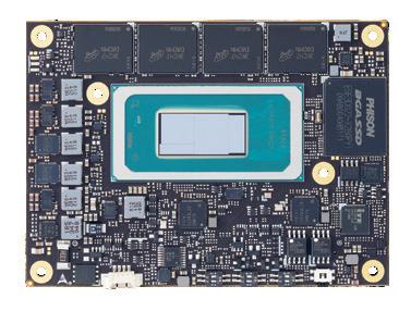
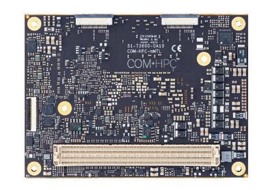
EMBEDDED MODULE
ADLINK has launched the COM-HPCmMTL — an innovative module that features Intel Core Ultra architecture and rich I/O capabilities. This makes it suitable for edge applications that require enhanced processing power and versatile connectivity.
The module is powered by the Intel Core Ultra architecture with up to 14 CPU cores, 8 Xe GPU cores and an integrated NPU for high-performance AI acceleration. It is designed for high-performance, energy efficient battery-powered applications, such as industrial automation, data loggers, UAVs (unmanned aerial vehicles), portable medical ultrasound devices and AI-powered robots.
The module features up to 64GB LPDDR5x memory soldered directly onto the board at speeds of 7467 MT/s, supporting maximum performance and efficiency. Its 95x70 mm size allows it to fit into constrained spaces, with a rugged operating temperature range from -40 to 85°C (for selected SKUs).
Despite its compact form factor, the embedded module integrates 16x PCIe lanes, 2 SATA interfaces, 2x 2.5GbE Ethernet ports and DDI/USB4, USB 3.0/2.0 interfaces, providing rich I/O options for demanding applications.
ADLINK offers the COM-HPCmMTL development kit for efficient prototyping and referencing, available in the second half of 2025.
ADLINK Technology Inc www.adlinktech.com
ROBOTICS CONTROLLER
Axiomtek has launched the ROBOX300, a compact and energy-efficient robotics controller designed for autonomous mobile robots (AMRs). Powered by the Intel Core i5-1145G7E processor with a 15 W TDP, the controller is designed to perform in challenging industrial environments with an operating temperature range of -40 to +60°C, and supports a broad voltage input of 9–60 VDC with Smart Ignition Management function. It also features USB power on/off control to enhance system stability and efficiency. The controller also comes pre-installed with Axiomtek’s ROS 2-based DigiHub for AMR software, simplifying robotic application development and integration for warehouse and factory automation.
The controller features dual 260-pin DDR4-3200 SO-DIMM slots, providing up to 64 GB of system memory capacity. With support for an optional 2.5 ″ SATA drive and one M.2 Key M 2280 socket for NVMe, this industrial computer provides ample storage for extensive data processing needs. Moreover, it features one M.2 Key E 2230 Wi-Fi/Bluetooth module and a full-size PCI Express Mini Card slot (USB + PCIe signal) for expanded connectivity options.
The device also features versatile I/O capabilities, including six serial ports (4-wire RS232: TX/RX/RTS/CTS, RS-422, RS-485) with isolated 1.5 kVDC, two CANbus with isolated 1.5 kVDC (supporting the CAN 2.0A and CAN 2.0B protocols), one 8-bit GPIO, two HDMI 1.4b ports, four USB 3.2 Gen1 ports, two USB 2.0 ports, three 2.5GbE LAN ports (Intel I226-IT), one RS-232 for console port, and six antenna openings. The robotics controller also supports Linux Ubuntu 22.04 LTS.
The ROS 2 AMR controller ROBOX300 is available now.
Tekdis www.tekdis.com.au
ELECTRONIC SYSTEMS DESIGN TECHNOLOGY
Siemens has launched its Xpedition Standard software, to make its AIenhanced electronic systems design technology more accessible to small and mid-sized businesses.
Built on Siemens’ Xpedition technology, this new offering combines intuitive user experiences, integrated cloud collaboration and AI-driven automation.
Xpedition Standard is built for growing teams that need a balance of cost-efficiency and advanced capabilities. It includes features like design reuse, variant management, advanced routing automation, native 3D layout and deeper collaboration across mechanical, manufacturing and supply chain stakeholders. Teams can further extend capabilities using token-based options, which provide on-demand access to more advanced capabilities such as fully integrated pre- and post-layout signal integrity analysis powered by Siemens’ Hyperlynx software for PCB analysis and rigid-flex design without requiring a full tier upgrade.
Part of the Siemens Xcelerator portfolio of industry software, the new technology is part of the Xpedition family and is designed to grow with engineers, from individual users to global enterprises. The unified user experience, design libraries and cloud-based collaboration infrastructure provide a straightforward upgrade path as team and project requirements evolve.
Siemens Digital Industries Software www.siemens.com.sg/en
NEWS from the SMCBA
The Widening Scope of SMCBA 2025 Electronics Design and Manufacturing Conference
electronics manufacturing industry through the challenges of the transition from through-hole to surface mount technology, from lead-containing solder alloys to lead-free solders, through the reduction in pitches and the increase in the number of layers of the printed circuit boards. The opening address of the conference was presented by Nadia Court, the director of the Semiconductor Sector Service Bureau (S3B) who introduced delegates to the wide range of activities underway in Australia directed at strengthening Australia’s sovereign capability in the electronics and semiconductor supply chain. Court was supported by Ben Kitcher, the Executive Director of the Advanced Manufacturing Facility (AMRF) that is being established in the scientific and industrial precinct that is developing in Bradfield, to develop the critical technologies required for semiconductor packaging.
Chuck Corley provided a definitive guide to the design of power delivery systems for modern power-hungry integrated circuits; Chris Turner provided a deep dive into the challenge of designing electronic circuitry for manufacture and testing; Jasbir Bath reviewed the challenges for electronics manufacturing in the next 10 years, as identified in the iNEMI Board Assembly Roadmap; and Dave Hillman shared with delegates what he has learned in a decade of practical experience in soldering bottom terminated components (BTC), particularly in defense and aerospace applications.
The team from Future Electronics presented a review of the challenges of component sourcing in difficult times. With supply chain security a growing issue in an unstable world, the initiator of the PCB Connect movement, Elexon Electronics, Frank Faller provided an update on the progress that has been made since this initiative began on the Queensland Sunshine Coast in February this year.
Undoubtedly those who attended this conference left with a wider and deeper understanding of the current issues in the key global industry of electronics manufacturing.
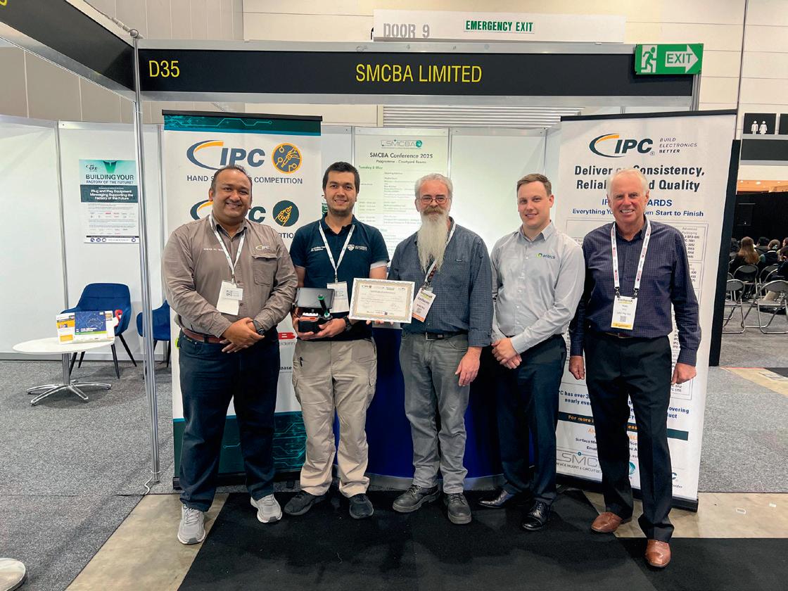
Those more concerned with the practicalities of hands-on soldering were given a chance to test their skills by the IPC Hand Soldering (HSC) and Wire Harness (WHC) Competitions conducted at the SMCBA booth on the floor of Electronex, adjoining the conference in the Melbourne Convention and Exhibition Centre. The winners of these contests are given the opportunity to compete in the final of the global competitions in Munich and Bengaluru, for the HSC and WHC competitions respectively.
Congratulations to this year’s winners – Tony from the Australian Centre for Robotics (ACFR) and and Sai from Design2000.
IPC becomes Global Electronics Association
In a global webinar on June 24 the IPC Board Chair, Tom Edman, the IPC President and CEO, John Mitchell and the Vice President Member services and Marketing, Brian Knier delivered the news that the IPC will now operate under the name Global Electronics Association with a new logo that reflects that global coverage.
While confirming that the organisation is still committed to the development of the manufacturing and quality standards on which the electronics industry relies and that the IPC Brand will be retained for these, it has been recognised that there was a need to acknowledge the much wider range of activities in which the organisation now engages. This growth in the scope of its activities has been a natural consequence of the rise of electronics manufacturing from a rather narrow specialty when the IPC began in 1957 to a US$6 trillion industry that is the foundation of the modern global economy with all the political consequences that come with that stature.
The IPC has been working in close partnership with the industry as it grew, wherever it was located. The new name, with a new logo, was chosen because it better reflects that reality. CEO John Mitchell made the point that the focus of the organisation is now primarily supply chain security because all electronics manufacturers, wherever they are located, rely on supply chains that can deliver high quality componentry in the required time frame, at competitive pricing in the quantities required. Those secure and reliable supply chains make it possible to manufacture high quality finished products wherever national strategic consideration dictate.
For the SMCBA, there are clear parallels with the concern about supply chain security in Australia that were identified in the PCB Connect initiative that began on the Sunshine Coast on February 26. The Global Electronics Association’s affiliate in Australia, the SMCBA will be fully engaging with these new initiatives, looking for opportunities for Australian manufacturers to find their place, as contributors and beneficiaries in the network of secure supply chains.
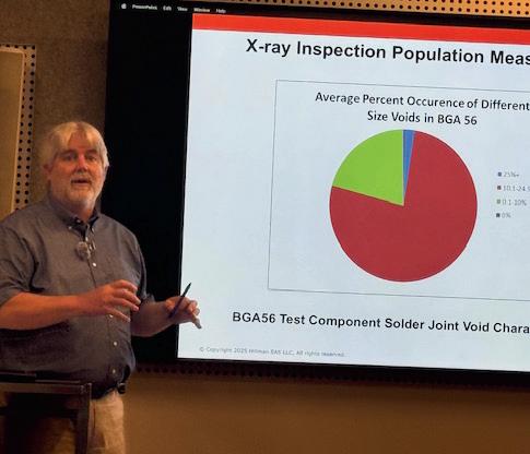
From left to right: Johnson (lead competition judge), Tony (award winner), Anthony (SMCBA), Brandon (Oritech), and Noel (ElectroneX).
Dave Hillman, presenting at SMCBA Conference.
CABLE DRUM CHANNELS
Adept Direct’s Cable Drum Channels offer a robust solution for managing heavy cable reels with ease. Designed to accommodate cable reels up to 1000 kg in weight and 1000 mm in width, the channels support reels with diameters ranging from 600 to 1800 mm. Each set comprises two heavy-duty nylon rollers mounted on a stabilising bar, allowing the drum to remain centred during cable payout.
The rollers are equipped with free-wheeling heavy-duty bearings, facilitating smooth and rapid unrolling of cables. A shallow ramp at one end allows for easy loading of large cable reels, while front rollers feature a locking mechanism to assist in rolling the cable drum back off the rollers once cabling is complete.
The channels are finished in a high-visibility Safety Yellow powder coat, enhancing site safety. Thumbscrews secure the channels onto the galvanised stabiliser axle, aligning them with the flanges of the cable drum. For added convenience, the channels can be paired with Adept Direct’s Forklift Cable Drum Attachment, enabling efficient loading and unloading of cable drums using a forklift or telehandler.
The cable drum channels are engineered to meet the needs of modern electrical installations. Their robust construction and compatibility with other Adept Direct products make them a suitable tool for professionals seeking to streamline cable handling processes.
Adept Direct www.adeptdirect.com.au
RUGGED TABLET
The RuggON SOL 7, a 12 ″ fully rugged Windows tablet powered by Intel Arrow Lake Core Ultra 5/7 processors, is suitable for Australian industries that operate in remote, harsh and mission-critical environments.
Purpose-built for sectors such as public safety, mining, agriculture, utilities, warehousing and fleet management, the tablet combines rugged durability with next-generation AI inferencing capabilities, ultra-fast connectivity and advanced data capture — all in a portable package.
Powered by Intel Core Ultra processors with Intel AI Boost, the tablet performs AI inferencing on-device. This means it can instantly analyse images, video or sensor data — enabling tasks like defect detection, facial recognition or licence plate matching in real time, even in disconnected environments.
The hot-swappable dual-battery design offers up to 11 h of runtime per cycle, with fast charging for enhanced productivity. Field workers can replace batteries without powering down, making the tablet suitable for round-the-clock shifts.
Certified to MIL-STD-810H and IP65, the tablet can operate in -20 to +63°C. It’s engineered to withstand drops, vibration, water, dust and extreme heat — making it suitable for Australian mining sites, construction zones and regional farms.
Equipped with Wi-Fi 7, 5G/LTE, dual SIM (SIM + eSIM) and SATCOM compatibility, the tablet keeps users connected in a range of locations. It also supports 2D barcode scanning (OCR), NFC with FIDO2, UHF RFID, smart card and fingerprint authentication.
The RuggON SOL 7 is available in Australia through Metromatics, offering local sales, integration and support from offices in Brisbane, Sydney and Melbourne. Metromatics Pty Ltd www.metromatics.com.au
RESEARCHERS CRACK SCALABLE CMOS QUANTUM COMPUTING
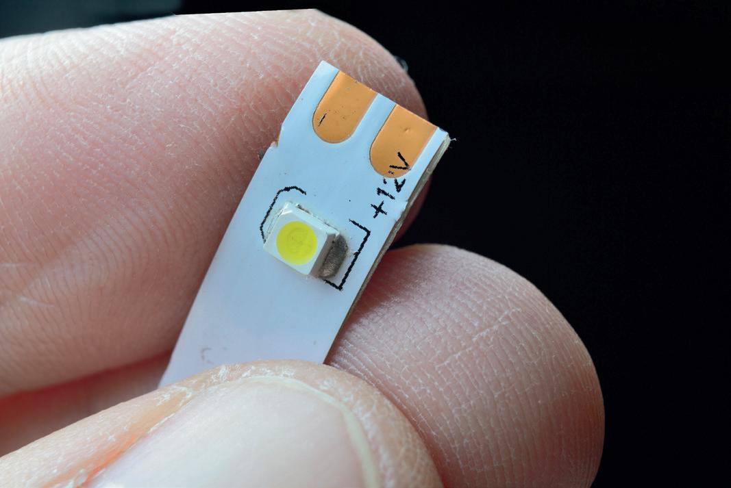
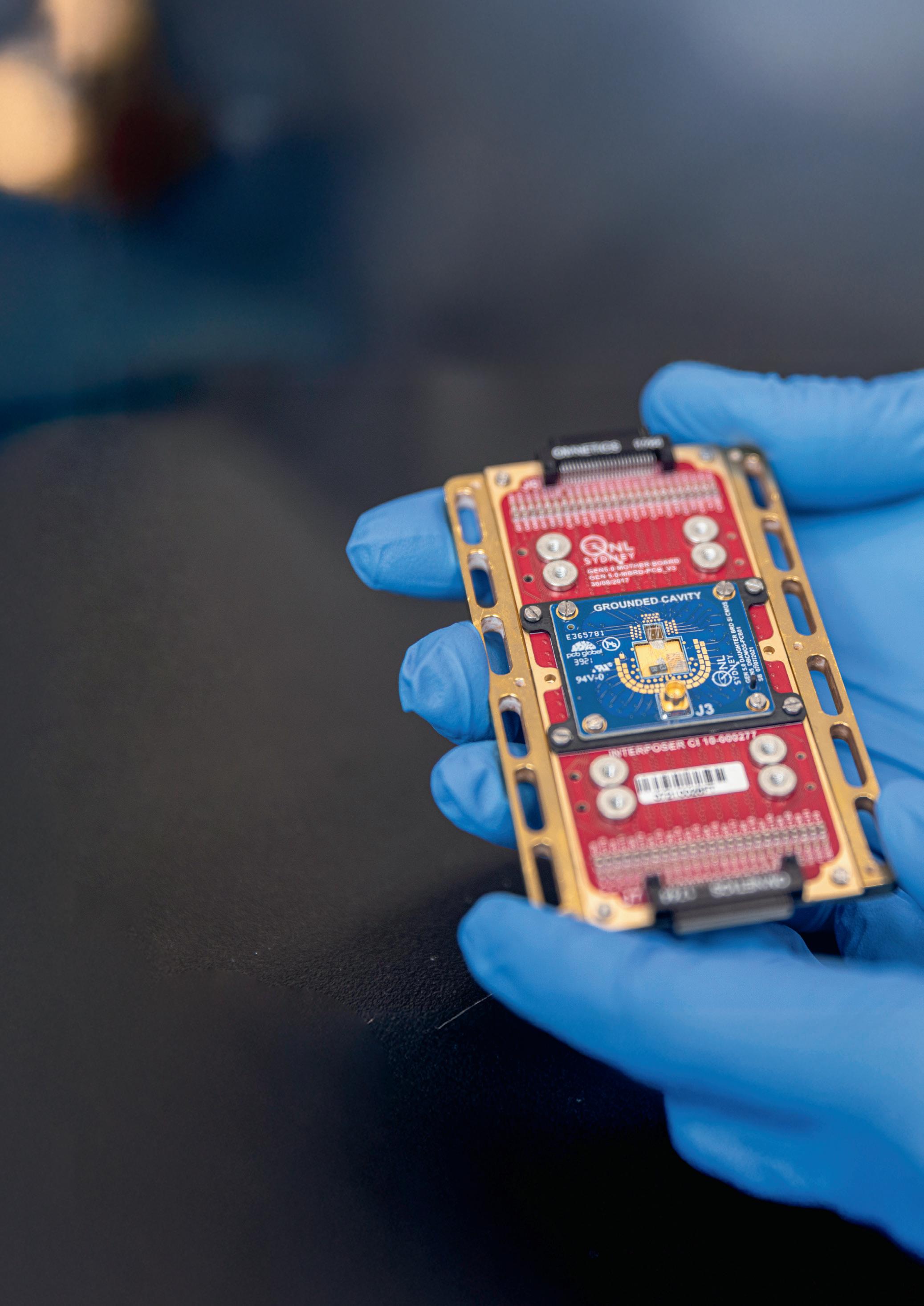
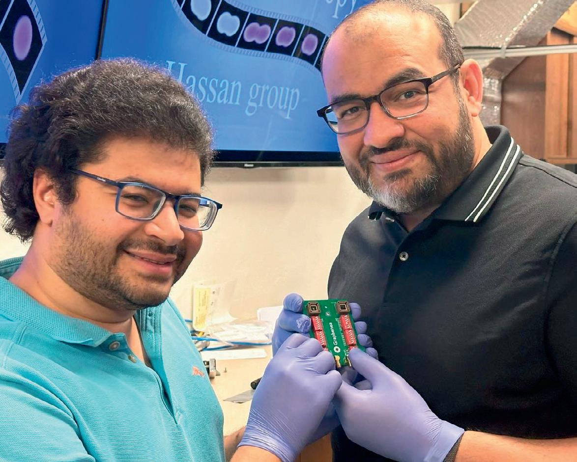
Developing technology that allows quantum information to be both stable and accessible is a critical challenge in the development of useful quantum computers that operate at scale. Research published in the journal Nature provides a pathway for scaling the number of quantum transistors (known as qubits) on a chip from current numbers under 100 to the millions needed to make quantum computation a practical reality. The result is enabled by new cryogenic control electronics that operate at close to absolute zero, developed at the University of Sydney.
Lead researcher Professor David Reilly from the University of Sydney Nano Institute and School of Physics said, “This will take us from the realm of quantum computers being fascinating laboratory machines to the stage where we can start discovering the real-world problems that these devices can solve for humanity.”
The paper is the result of industry cooperation between the University of Sydney and the University of New South Wales through respective quantum tech spin-out companies Emergence Quantum and Diraq. Reilly’s company Emergence Quantum was established this year to commercialise quantum control technologies and other advanced electronics, just like the chip presented in this Nature paper.
For this research, his team developed a silicon chip that can control spin qubits at milli-kelvin temperatures. That’s just slightly above absolute zero (-273.15°C), the temperature at which — theoretically — matter ceases moving.
Fiona Wolf.
Quantum control chip developed by Professor David Reilly’s team.
QUANTUM PROCESSORS
Of the many emerging qubit technologies, experts think that spin qubits (where information is encoded onto the magnetic direction of single electrons) could more easily scale up as they are based on common CMOS (complementary metal-oxide-semiconductor) technology that underpins modern conventional computing and is already used to print billions of transistors.
Semiconductor control system integrated with qubits
However, spin qubits must be kept at temperatures below 1 kelvin to preserve their information. To scale up, they also need to be controlled and measured using complex, integrated electronics. This created a real concern that even if you could get the control system to work at that temperature, the heat and electrical interference generated by placing the control so close to the qubits would degrade their performance.
Reilly’s team has, for the first time, shown that with careful design this need not be the case — a vital proof-of-principle demonstration that spin qubits in CMOS could be scaled up to the millions of qubits to make a useful machine.
Reilly said, “This result has been more than a decade in the making, building up the know-how to be able to design electronic systems that dissipate tiny amounts of power and operate near absolute zero. We have now demonstrated a scalable control platform that can be integrated with qubits without destroying the fragile quantum states.
“This validates the hope that indeed qubits can be controlled at scale by integrating complex electronics at cryogenic temperatures. Our paper shows that with careful design of the control system, fragile qubits hardly notice the switching of transistors in a chip less than a millimetre away.”
Good science, good commercialisation
The qubits were supplied by Diraq, a UNSW spin-out established by Professor Andrew Dzurak, and the know-how that enabled the University of Sydney-designed control chip will now carry over to underpin much of the work of the new company, Emergence Quantum, co-founded by Reilly and Dr Thomas Ohki.
“As well as good science, this is a good commercialisation story, too, and is more evidence why Sydney is a vital cog in the global quantum industry,” Reilly said.
Lead author Dr Sam Bartee, who undertook experiments as a PhD student with Reilly at the University of Sydney, is now working at Diraq. “It’s extremely exciting to be part of this work, to be involved in the development of such powerful technologies and to sit in this hotspot of quantum computing research. Sydney really is a remarkable place to be a quantum engineer at the moment,” Bartee said.
Dr Kushal Das was the lead designer of the control chip. He holds a joint position with the University of Sydney and Emergence Quantum. “Now that we have shown that milli-kelvin control does not degrade
the performance of single- and two-qubit quantum gates, we expect many will follow our lead. Fortunately for us, this is not so easy but requires years to build up the know-how and expertise to design low-noise cryogenic electronics that needs only tiny amounts of power,” Das said.
Reilly added, “Here we are showing the impact that cryogenic electronics can have on scaling up qubits, but we see many further diverse applications for this technology, spanning near-term sensing systems to the data centres of the future.”
Technical details
Bartee and his co-authors measured the performance characteristics of one- and two-qubit operations controlled by the cryoCMOS chiplet. They compared its performance against that of a standard cable-connected room-temperature control system.
Their findings include:
• negligible fidelity loss for single-qubit operations;
• no measurable reduction of the coherence time for one- and two-qubit operations;
• comparable behaviour of qubit interactions, indicating negligible interference from electrical noise.
Remarkably, these feats were achieved within a power envelope of just 10 microwatts, the vast majority of which was expended on the digital systems. The analog components dissipate only around 20 nanowatts per megahertz, which means that the system can be scaled up to millions of qubits without a significant increase in power usage.
“THIS WILL TAKE US FROM THE REALM OF QUANTUM COMPUTERS BEING FASCINATING LABORATORY MACHINES TO THE STAGE WHERE WE CAN START DISCOVERING THE REAL-WORLD PROBLEMS THAT THESE DEVICES CAN SOLVE FOR HUMANITY.” DAVID REILLY.
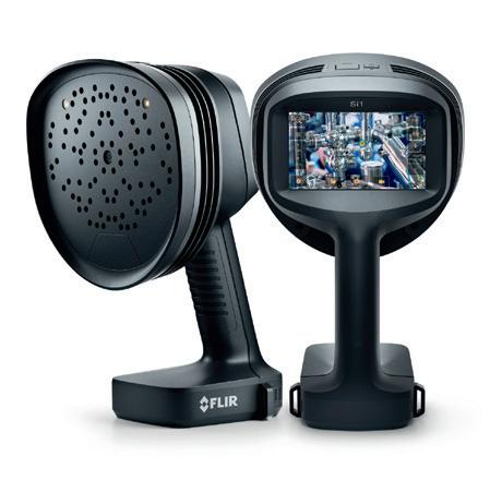
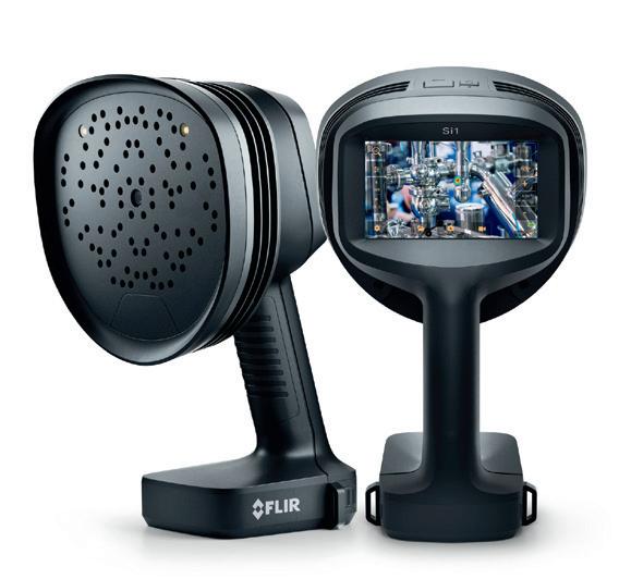
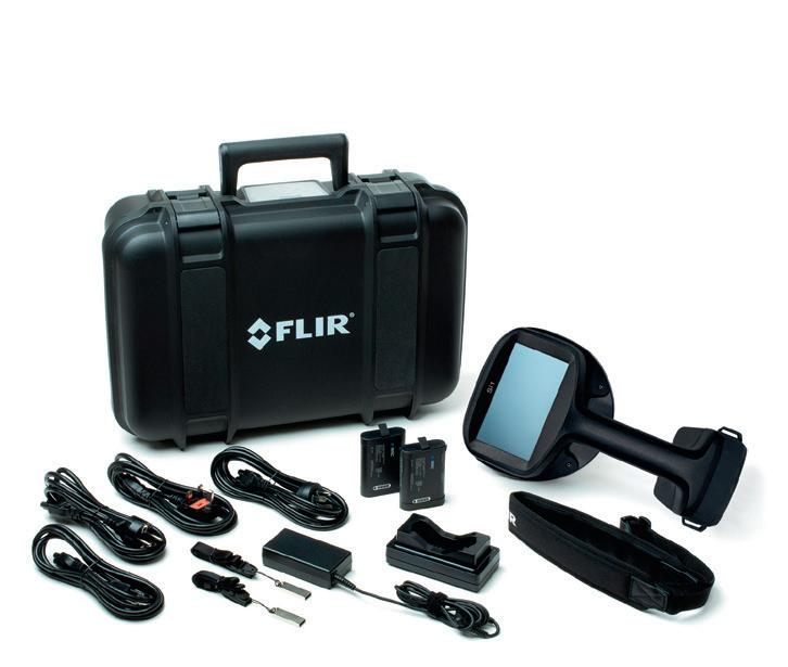
ACOUSTIC IMAGING CAMERA
FLIR, a Teledyne Technologies company, has launched the Si1-LD, an industrial acoustic imaging camera that brings faster and more accurate compressed air leak detection to condition monitoring. The acoustic imaging camera features enhanced detection and quantification capabilities in comparison with the existing FLIR Si124-LD Plus, along with a higher upper limit frequency range.
Leveraging the advantages of ultrasonic technology, the acoustic imaging camera pinpoints leaks with enhanced imaging sensitivity. It also offers a number of stand-out capabilities and features, such as an array of 96 microphones (2–100 kHz) to facilitate the automatic detection, location and measurement of compressed air and vacuum leaks from a safe distance of up to 130 m. Support comes from a 12 MP colour camera with 8x digital zoom and LED lamp, facilitating the easy capture of visual details.
Bandpass filtering allows inspectors to tune out any confusing and/or incorrect sources of ultrasound without manual tuning. The acoustic imaging camera is also suitable for challenging leak detection applications where user input is advantageous; the inspector can use the bandpass filter to undertake manual tuning of the required frequency range.
The touch-screen interface displays high-resolution images for easy issue identification with real-time, on-device quantification in terms of leak volume flow rate and leak cost per year. Users can leverage this data to prioritise repairs. The data is also suitable for inclusion in sustainability reports as an indication of energy reduction initiatives.
Wireless data transfer facilitates seamless reporting/analytics options, using either the online FLIR Acoustic Viewer or offline FLIR Thermal Studio data backup and organisational team sharing, while also providing the backbone for over the air (OTA) firmware updates. The software gives users the ability to create reports through pre-built or fully customisable templates.
The acoustic imaging camera comes with two batteries, additional battery cover, battery charger, camera neck strap, hard case, USB memory stick, access to free versions of online & offline acoustic analysis and reporting software, and two-year warranty. Users can also upload their acoustic images into FLIR Thermal Studio software or the FLIR Acoustic Viewer.
Two versions of the Si1-LD are available, with and without Wi-Fi. All other features are the same.
Teledyne e2v Asia Pacific Limited www.teledyne-e2v.com
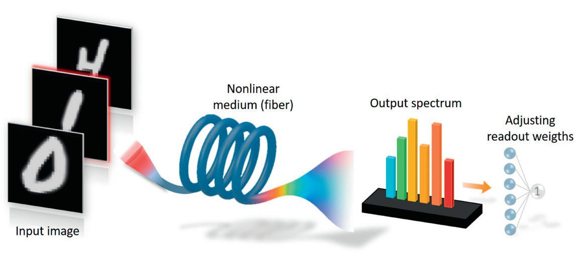
OPTICAL FIBRES PROCESS DATA AT ULTRA-FAST SPEEDS
Tampere University
Imagine a computer that does not rely only on electronics but uses light to perform tasks faster and more efficiently. Two research teams from Finland and France have now demonstrated a novel way to process information using light and optical fibres, opening up the possibility to build ultra-fast computers.
The study, performed by postdoctoral researchers Dr Mathilde Hary from Tampere University and Dr Andrei Ermolaev from the Université Marie et Louis Pasteur, Besançon, demonstrated how laser light inside thin glass fibres can mimic the way artificial intelligence (AI) processes information. Their work has investigated a particular class of computing architecture known as an Extreme Learning Machine, an approach inspired by neural networks.
“Instead of using conventional electronics and algorithms, computation is achieved by taking advantage of the nonlinear interaction between intense light pulses and the glass,” Hary and Ermolaev said.
Traditional electronics approaches its limits in terms of bandwidth, data throughput and power consumption. AI models are growing larger, they are more energyhungry, and electronics can process data only up to a certain speed. Optical fibres, on the other hand, can transform input signals at speeds thousands of times faster and amplify tiny differences via extreme nonlinear interactions to make them discernible.
Towards efficient computing
In their recent work, the researchers used femtosecond laser pulses (a billion times shorter than a camera flash) and an optical fibre confining light in an area smaller than a fraction of human hair to demonstrate the working principle of an optical ELM system. The pulses are short enough to contain a large number of different wavelengths or colours. By sending those into the fibre with a relative
delay encoded according to an image, they show that the resulting spectrum of wavelengths at the output of the fibre transformed by the nonlinear interaction of light and glass contains sufficient information to classify handwritten digits (like those used in the popular MNIST AI benchmark). According to the researchers, the best systems reached an accuracy of over 91%, close to state-of-art digital methods, in under one picosecond.
Schematic of optical extreme learning machine using nonlinear fibre-optics propagation.
Mathilde Hary.
What is remarkable is that the best results did not occur at maximum level of nonlinear interaction or complexity; but rather from a delicate balance between fibre length, dispersion (the propagation speed difference between different wavelengths) and power levels.
“Performance is not simply a matter of pushing more power through the fibre. It depends on how precisely the light is initially structured; in other words, how information is encoded and how it interacts with the fibre properties,” Hary said.
By harnessing the potential of light, this research could pave the way towards new ways of computing while exploring routes towards more efficient architectures.
“Our models show how dispersion, nonlinearity and even quantum noise influence performance, providing critical knowledge for designing the next generation of hybrid optical–electronic AI systems,” Ermolaev said.
Advancing optical nonlinearity through collaborative research in AI and photonics
Both research teams are internationally recognised for their expertise in nonlinear light–matter interactions. Their collaboration brings together theoretical understanding and state-of-the-art experimental capabilities to harness optical nonlinearity for various applications.
“This work demonstrates how fundamental research in nonlinear fibre optics can drive new approaches to computation. By merging physics and machine learning, we are opening new paths toward ultrafast and energy-efficient AI hardware,” said Professors Goëry Genty from Tampere University, John Dudley and Daniel Brunner from the Université Marie et Louis Pasteur, who led the teams.
The research combines nonlinear fibre optics and applied AI to explore new types of computing. In the future the aim would be to build on-chip optical systems that can operate in real time and outside the lab. Potential applications range from real-time signal processing to environmental monitoring and high-speed AI inference.
iStock.com/Thomas-Soellenier
SPOTTING BAD BATTERIES BEFORE THEY MALFUNCTION
An uptick in battery-related fires has drawn attention to the challenge of identifying defects that can cause these catastrophic malfunctions, but are rarely obvious to the naked eye. In hopes of preventing the dangerous glitches that can cause batteries to overheat and catch fire, researchers from Drexel University have developed a standard testing process to give manufacturers a better look at the internal workings of batteries.
In a paper published in the journal Electrochimica Acta , the group presented methods for using ultrasound to monitor the electrochemical and mechanical functions of a battery — which would immediately reveal any damage or flaws that could lead to overheating and even cause thermal runaway.
“While lithium-ion batteries have been studied for nearly half a century and commercialised for over 30 years, we have only recently developed tools that can see inside with high resolution,” said Wes Chang, PhD, an assistant professor and primary investigator of the Battery Dynamics Lab in Drexel’s College of Engineering, who supervised the project. “In particular, ultrasound has been adapted from other fields, such as geophysics and biomedical sciences, for battery diagnostics only in the past decade. Because it is such a new technique in the battery and electric vehicle industries, there is a need to teach battery engineers how it works and why it is useful,” Chang said.
The team’s work strives to do this, by demonstrating a low-cost, accessible benchtop
ultrasonic tool that it hopes can be easily implemented and used by battery engineers, including those who work at automotive companies producing electric vehicles.
According to a Consumer Affairs report, individuals use three to four electronic devices powered by batteries each day — from laptops, phones and tablets, to power tools and electric transit, like bikes and scooters — a number that has doubled in the last five years. The rush to supply batteries for all of these devices has created a market for products that can be produced cheaper and faster. This is a concern, according to Chang, because it may allow low-quality cells to enter the market.
“While the vast majority of lithium-ion batteries today are high performing and safe, defects are bound to exist when thousands of cells are used within electric vehicles and there are millions of electric vehicles being produced every year,” Chang said.
The current safety and quality control processes for manufactured batteries rely heavily on visual inspection and performance testing of select battery cells after they come
off the line. Manufactured batteries may also be X-rayed to generate a high-resolution interior image, but this is slow and expensive.
Manufacturers are required to follow these inspection and testing protocols, but with the scale at which batteries are being used, even a small design or manufacturing flaw that is missed can lead to a massive batch of defective batteries making their way into market.
By contrast, the method proposed by the Drexel team uses acoustic imaging — ultrasound — which is faster and less expensive than X-rays and can provide complementary information about the mechanical properties of the battery. Chang’s group reported using scanning acoustic microscopy technology to send low-energy sound waves through a commercial pouch cell battery.
Without affecting its internal operations or affecting its performance, the speed of the waves is altered as it passes through the various materials inside a battery. This allows researchers to get a complete, detailed and quick look at the chemical changes within battery materials as it is being used.
“By observing how the sound wave has changed upon interacting with the sample, we can deduce a number of structural and mechanical features,” they wrote in the report.
The process can help to detect structural defects or damage that could cause an electrical short, material deficiencies or imbalances that could hamper performance, as well as indicators that problems are likely to occur. One substance the scan is particularly good at detecting is gas, which is important because the presence of gas inside a battery is an indication of dry areas that could cause the cell to fail while it is being used.
The sensitivity of ultrasound makes it useful not just for detecting defects in manufacturing, but also for gauging how new battery chemistries fail in research and development labs. As part of the research, Chang’s group worked with research partners at SES AI, a lithium metal battery startup company. Deploying the testing platform at SES AI’s research and development site gave the engineers instantaneous access to data during the design and testing process
which allowed them to make adjustments and corrections more quickly.
In addition to reporting their process for the ultrasound testing method, the team also developed open-source software to run the instrument and produce a rapid analysis of the resulting data.
“We hope that by lowering the barrier to entry, ultrasonic testing can become a routine part of battery research and development,” Chang said. “Battery scientists want to build better batteries, not develop new tools. We provide a user interface that is easy to use, with regular software updates. This adds to the existing collection of tools that battery scientists have on hand for measuring and diagnosing next-generation battery performance.”
The group plans to continue improving the technology so that it can more easily scan battery electrodes, as well as cells, and produce more detailed three-dimensional images rather than the currently limited twodimensional scans to better detect defects.
This is a modified version of a news item published by Drexel University.
RUGGED LAPTOP
Getac Technology Corporation has launched the Getac B360 Plus Copilot+ PC, a fully rugged laptop. Featuring the latest Windows AI technology, this new device extends Getac’s B360 and B360 Pro line-up, designed for professionals working in industries such as defence, utilities, public safety and manufacturing.
Featuring a neural processing unit (NPU) capable of up to 48 trillion operations per second (TOPS), the device offers enhanced AI performance, enabling users to excel in extreme work environments and high-pressure scenarios.
By expanding its AI solution line-up with the B360 Plus, Getac continues to meet the needs of customers around the world, helping them solve challenges and achieve their operational objectives.
Rugged AI-ready devices equipped with image recognition solutions allow industry professionals to conduct realtime inspections, detect anomalies and predict potential equipment failures in the field, preventing unplanned downtime and improving service stability. Manufacturing organisations can remotely monitor their factory environments in real time through a combination of edge computing technology and image recognition AI solutions. Doing so enables them to identify worker safety issues, compliance breaches and potential maintenance concerns at the earliest opportunity, helping cut maintenance costs and reduce risk.
Getac Technology Corp
www.getac.com
iStock.com/Tero
Vesalainen
CABINET COOLER SYSTEMS
EXAIR’s ATEX Cabinet Cooler Systems provide a powerful solution for keeping electrical enclosures cool in hazardous ATEX classified areas — and they’re now available in durable aluminium construction. Engineered for use in Zones 2 and 22, these coolers are UL tested and CE compliant, and they meet ATEX standards for purged and pressurised enclosures.
With cooling capacities of up to 5600 BTU/h, the cabinet coolers are suitable for preventing overheating in electrical cabinets exposed to explosive atmospheres. Whether users are dealing with industrial control panels, application-specific electrical boxes or simply sensitive electronics in hazardous locations, these systems enable equipment to stay cool, safe and operational. Designed for quick and easy installation, the cabinet cooler mounts through a standard electrical knockout and maintains NEMA 4 (IP66) integrity even in demanding environments. Optional thermostat control reduces compressed air usage, while cold air distribution kits facilitate even cooling throughout the cabinet.
Compressed Air Australia offers a comprehensive line-up of EXAIR Cabinet Cooler Systems for NEMA 12, 4, 4X, hazardous location and ATEX applications. Built with no moving parts, every system is CE compliant, UL listed and designed for long-term use in a range of challenging conditions. From control panels and motor centres to laser housings and surveillance equipment, EXAIR Cabinet Coolers are designed to keep operations running smoothly.
Compressed Air Australia Pty Ltd www.caasafety.com.au
GNSS MODULE
Quectel Wireless Solutions has launched the LG680P, a multi-constellation, quad-band GNSS module designed to deliver high-precision positioning across a range of applications including precision agriculture, intelligent robots and surveying.
The GNSS module is designed to receive signals from multiple global navigation satellite systems, including GPS, GLONASS, Galileo, BeiDou (BDS), QZSS and NavIC, for enhanced positioning accuracy. With multi-band GNSS support, it concurrently receives L1, L2 and L5 bands, boosting signal quality and precision. The module will also support Galileo E6, QZSS L6 and BDS B2b for Precise Point Positioning (PPP) technology, delivering accuracy without requiring local or broadband connectivity.
The LG680P is designed to achieve horizontal accuracy of up to 0.8 cm + 1 ppm, for stable performance even in challenging urban environments. The module has also been tested with dual-band corrections, for backward compatibility with existing systems that rely on dual-band technology. While quad-band corrections provide the most optimised performance, this capability allows the module to replace older dual-band systems, offering enhanced precision and futureproofing without requiring immediate infrastructure changes.
The GNSS module also features professional-grade anti-jamming and interference detection algorithms, maintaining signal integrity even in complex electromagnetic environments. Its built-in NIC anti-jamming technology suppresses multiple narrow-band interferences, enhancing signal reception and stability. The module also supports fast positioning updates with a refresh rate of up to 20 Hz, enabling real-time tracking and improved responsiveness.
With a 22 x 17 mm footprint, the module adopts a widely used industry form factor and supports multiple interfaces, including UART, SPI, I2C and CAN. The module is also designed for optimised signal reception, with support for external active antennas to enhance positioning accuracy. Additionally, its low power consumption makes it an energy-efficient solution suitable for battery-operated devices.
Quectel www.quectel.com
PETAHERTZ-SPEED PHOTOTRANSISTOR FOR
AMBIENT CONDITIONS
Logan Burtch-Buus, University of Arizona Communications
What if ultra-fast pulses of light could operate computers at speeds a million times faster than today’s best processors? A team of scientists, including researchers from the University of Arizona, are working to make that possible.
In a ground-breaking international effort, researchers from the Department of Physics in the College of Science and the James C. Wyant College of Optical Sciences have demonstrated a way to manipulate electrons in graphene using pulses of light that last less than a trillionth of a second. By leveraging a quantum effect known as tunnelling, they recorded electrons bypassing a physical barrier almost instantaneously,
a feat that redefines the potential limits of computer processing power.
The study, published in Nature Communications , highlights how the technique could lead to processing speeds in the petahertz range — over 1000 times faster than modern computer chips.
“Sending data at those speeds could revolutionise computing as we know it,” said Mohammed Hassan, an associate professor of physics and optical sciences. Hassan has long pursued light-based computer technology and previously led efforts to develop the world’s fastest electron microscope.
“We have experienced a huge leap forward in the development of technologies like artificial intelligence software, but the speed of hardware development does not move as quickly,” Hassan said. “But, by leaning on the discovery of quantum computers, we can develop hardware that matches the current revolution in information technology software. Ultrafast computers will greatly assist discoveries in space research, chemistry, health care and more.”
Hassan worked alongside U of A colleagues Nikolay Golubev, an assistant professor of physics; Mohamed Sennary, a graduate student studying optics and physics; Jalil Shah, a postdoctoral scholar of physics; and Mingrui Yuan, an optics graduate student. They were joined by colleagues from the California Institute of Technology’s Jet Propulsion Laboratory and the Ludwig Maximilian University of Munich in Germany.
The team was originally studying the electrical conductivity of modified samples
“THIS ACHIEVEMENT REPRESENTS A BIG LEAP FORWARD IN THE DEVELOPMENT OF ULTRAFAST COMPUTER TECHNOLOGIES.” MOHAMMED HASSAN.
Mohammed Hassan (right), associate professor of physics and optical sciences, and Mohamed Sennary, a graduate student studying optics and physics, holding the commercial transistor they used to develop a petahertz-speed transistor.
of graphene, a material composed of a single layer of carbon atoms. When a laser shines on graphene, the energy of the laser excites electrons in the material, making them move and form into a current.
Sometimes, those electric currents cancel each other out. Hassan said this happens because the laser’s energy wave moves up and down, generating equal and opposite currents on either side of the graphene. Because of graphene’s symmetrical atomic structure, these currents mirror each other and cancel each other out, leaving no detectable current.
But what if a single electron could slip through the graphene, and its journey could be captured and tracked in real time? That near-instant “tunnelling” was the unexpected
result of the team modifying different graphene samples.
“That is what I love most about science: the real discovery comes from the things you don’t expect to happen,” Hassan said. “Going into the lab, you always anticipate what will happen — but the real beauty of science are the little things that happen, which lead you to investigate more. Once we realised that we had achieved this tunnelling effect, we had to find out more.”
Using a commercially available graphene phototransistor that was modified to introduce a special silicon layer, the researchers used a laser that switches off and on at a rate of 638 attoseconds to create what Hassan called “the world’s fastest petahertz quantum transistor”.
A transistor is a device that acts as an electronic switch or amplifier that controls the flow of electricity between two points and is fundamental to the development of modern electronics.
“For reference, a single attosecond is one-quintillionth of a second,” Hassan said. “That means that this achievement represents a big leap forward in the development of ultrafast computer technologies by realising a petahertz-speed transistor.”
While some scientific advancements occur under strict conditions, including temperature and pressure, this new transistor performed in ambient conditions — opening the way to commercialisation and use in everyday electronics.
Hassan is working with Tech Launch Arizona, the office that works with investigators to commercialise inventions stemming from U of A research in order to patent and market innovations. While the original invention used a specialised laser, the researchers are furthering development of a transistor compatible with commercially available equipment.
“I hope we can collaborate with industry partners to realise this petahertz-speed transistor on a microchip,” Hassan said. “The University of Arizona is already known for the world’s fastest electron microscope, and we would like to also be known for the first petahertz-speed transistor.”
Silicon is king in the semiconductor technology that underpins smartphones, computers, electric vehicles and more, but its crown may be slipping, according to a team led by researchers at Penn State. The researchers have used two-dimensional (2D) materials, which are only an atom thick and retain their properties at that scale, unlike silicon, to develop a computer capable of simple operations.
The development, published in Nature , represents a major leap towards the realisation of thinner, faster and more energy-efficient electronics, the researchers said. They created a complementary metal-oxide semiconductor (CMOS) computer — technology at the heart of nearly every modern electronic device — without relying on silicon. Instead, they used two different 2D materials to develop both types of transistors needed to control the electric current flow in CMOS computers: molybdenum disulfide for n-type transistors and tungsten diselenide for p-type transistors.
“Silicon has driven remarkable advances in electronics for decades by enabling continuous miniaturisation of field-effect transistors (FETs),” said Saptarshi Das, the Ackley Professor of Engineering and professor of engineering science and mechanics at Penn State, who led the research. FETs control current flow using an electric field, which is produced when a voltage is applied. “However, as silicon devices shrink, their performance begins to degrade. Two-dimensional materials, by contrast, maintain their exceptional electronic properties at atomic thickness, offering a promising path forward.”
Das explained that CMOS technology requires both n-type and p-type semiconductors working together to achieve high performance at low power consumption — a key challenge that has stymied efforts to move beyond silicon. Although previous studies demonstrated small circuits based on 2D materials, scaling to complex, functional computers had remained elusive, Das said.
“That’s the key advancement of our work,” Das said. “We have demonstrated a CMOS computer built entirely from 2D materials, combining large area grown molybdenum disulfide and tungsten diselenide transistors.”
The team used metal-organic chemical vapour deposition (MOCVD) — a fabrication
2D, NON-SILICON COMPUTER UNVEILED
Ashley WennersHerron, Penn State University
process that involves vaporising ingredients, forcing a chemical reaction and depositing the products onto a substrate — to grow large sheets of molybdenum disulfide and tungsten diselenide and fabricate over 1000 of each type of transistor. By carefully tuning the device fabrication and post-processing steps, they were able to adjust the threshold voltages of both n- and p-type transistors, enabling the construction of fully functional CMOS logic circuits.
“Our 2D CMOS computer operates at lowsupply voltages with minimal power consumption and can perform simple logic operations at frequencies up to 25 kilohertz,” said first author Subir Ghosh, a doctoral student pursuing a degree in engineering science and mechanics under Das’s mentorship.
Ghosh noted that the operating frequency is low compared to conventional silicon CMOS circuits, but their computer — known as a one instruction set computer — can still perform simple logic operations.
“We also developed a computational model, calibrated using experimental data and incorporating variations between devices, to project the performance of our 2D CMOS computer and benchmark it against state-of-the-art silicon technology,” Ghosh said. “Although there remains scope for further optimisation, this work marks a significant milestone in harnessing 2D materials to advance the field of electronics.”
Das agreed, explaining that more work is needed to further develop the 2D CMOS computer approach for broad use, but also emphasising that the field is moving quickly when compared to the development of silicon technology.
“Silicon technology has been under development for about 80 years, but research into 2D materials is relatively recent, only really arising around 2010,” Das said. “We expect that the development of 2D material computers is going to be a gradual process, too, but this is a leap forward compared to the trajectory of silicon.”
This conceptual illustration of a computer based on 2D molecules displays an actual scanning electron microscope image of the computer fabricated by a team by researchers at Penn State. The keyboard features highlighted keys labelled with the abbreviations for molybdenum disulfide and tungsten diselenide, representing the two 2D materials used to develop the transistors in the computer.
WIRELESS MODULES
u-blox has introduced six new variants of the NORA-B2 Bluetooth Low Energy modules. Now integrating the entire range of Nordic Semiconductor’s nRF54L series of ultralow-power wireless systems-on-chip (SoCs), NORA-B2 offers a versatile solution for mass market segments due to its choices of antennas, architectures and chipsets.
The wireless modules combine ultralow power consumption and high processing efficiency, consuming up to 50% less current than previousgeneration devices while doubling process capacity. They also offer a range of security features, making them suitable for a variety of IoT applications, such as smart home devices, industrial automation and health care. The NORA-B2 series comprises four variants that differ in memory sizes and design architectures to match almost any device manufacturer’s requirements.
NORA-B20 uses the ultralow-power nRF54L15 SoC and integrates a 128 MHz Arm Cortex-M33 processor, a RISC-V co-processor and an ultralow-power multiprotocol 2.4 GHz radio. It comes with 1.5 MB of non-volatile memory (NVM) and 256 KB RAM.
NORA-B21, based on the ultralow-power nRF54L10 SoC, is designed for mid-range applications. It has 1 MB of NVM and 192 KB of RAM and can handle multiple wireless protocols simultaneously, including Bluetooth LE, Bluetooth Mesh, Thread, Matter, Zigbee and Amazon Sidewalk.
NORA-B22 is designed for cost-sensitive applications but still provides access to up to 31 GPIOs. It offers 0.5 MB of NVM and 96 KB of RAM.
NORA-B26 is designed for customers using the Network Co-Processor architecture and comes pre-flashed with the u-blox u-connectXpress software, allowing customers to integrate Bluetooth connectivity into their products with no prior knowledge of Bluetooth LE or wireless security.
All modules are designed for PSA Certified Level 3 security. They incorporate features such as secure boot and updates, tamper detection and secure firmware over-the-air (FOTA) updates. These security measures are designed to protect IoT devices against any potential threats, safeguarding data and functionality. The modules are also qualified against Bluetooth Core 6.0 that includes Channel Sounding, enabling endless possibilities in tracking and locating use cases.
NORA-B2 variants either come with an antenna pin for connecting an external antenna of choice or are designed with a patented PCB antenna for enhanced RF performance. All module versions come with global certification allowing device manufacturers to launch their products worldwide.
u-blox Singapore Pte Ltd www.u-blox.com
ANDROID TABLET
Getac has launched its next-generation ZX10 10-inch fully rugged Android tablet, which combines lightweight design with AI-ready performance and intuitive Android functionality for enhanced performance in the field. The tablet is suitable for professionals working in industries such as public safety, utilities, and transportation and logistics.
The tablets feature Qualcomm’s QCS6490 processor and neural processor unit (NPU), which are designed to support advanced AI capabilities. Additional features include advanced memory (8 GB LPDDR5) for fast data transfer and up to 256 GB universal flash storage (UFS) for a smooth user experience when running multiple applications simultaneously. The device also features an upgraded 1000 nits LumiBond screen with sunlight readable technology and capacitive multi-touch display, for effective operation in the rain and while wearing gloves. An optional active digitiser with stylus is also available for fast note taking and data entry in heavy rain and/or low temperatures.
The tablet includes dual SIM technology (Nano SIM + eSIM) for optimal mobile network coverage, while Wi-Fi 6E, Bluetooth 5.2 and optional dedicated dual-band GPS offer rapid data transfer and location positioning capabilities. For those with more extensive data collection and communication needs, the device can be configured with 4G LTE and 5G Sub-6, near field communication (NFC) (non-payment) and a barcode reader.
The tablet also features a hot-swappable dual-battery design that supports full-shift operation without downtime or delays. It can also be configured with a single battery for customers who wish to mount the device on forklifts or other vehicles. Optional high-capacity Li-ion battery packs are available for those who require longer battery life.
The tablet comes with MIL-STD-810H certification, IP66 certification and 6-foot drop resistance. It also has an operating temperature range of -29 to 63°C to provide peace of mind in adverse weather conditions.
The ZX10 tablet is powered by the intuitive Android operating system (Android 13 is installed as standard), for versatility and ease of use. It is also verified as an Android enterprise recommended rugged device, meeting all the specifications and requirements of Google’s testing process. This means it will receive full security updates every 90 days for five years after the launch date, along with regular patches and feature enhancements over this period.
Getac Technology Corp www.getac.com
CAN AI SPEED UP
CRITICAL COMMUNICATIONS CHIP DESIGN?
Radio frequency integrated circuits (RFIC) are critical to advancing communications capabilities — think moving from 5G networks to 6G — and many other technological applications. But these chips are also really hard to design.
Amulti-university team with heavy involvement from industry leaders is working to change that. The team, led by researchers from The University of Texas at Austin, plans to infuse artificial intelligence into the design process for RFICs to reduce the difficulty of making these important chips.
“Design productivity is a huge problem for RFICs; in most cases, it takes at least months to design a single chip,” said David Pan, professor in the Cockrell School of Engineering’s Chandra Family Department of Electrical and Computer Engineering and the project’s principal investigator. “Our goal is to significantly enhance design productivity by reducing development time and cost through an AI-assisted design flow, while also lowering the experience barrier for performing RFIC designs.”
To support this research, the team received a $9.6 million, 30-month award from Natcast, a non-profit that operates the National Semiconductor Technology Center (NSTC). The centre is a consortium established by the CHIPS and Science Act of 2022 to help bolster all aspects of semiconductor production in the United States. The award is one of three, totalling approximately $30 million, and the first ever through the NSTC’s Artificial Intelligence Driven Radio Frequency Integrated Circuit Design Enablement program. The cen-
tre is a consortium established by the CHIPS and Science Act to help bolster all aspects of semiconductor production in the United States.
The research
Titled “GENIE-RFIC: Generative ENgine for Intelligent and Expedited RFIC Design,” the project targets both silicon complementary metal oxide semiconductor (CMOS) RFICs and gallium nitride (GaN) monolithic microwave integrated circuits (MMICs). The AI-driven tools will perform rapid “inverse” designs based on target specifications, optimising circuit topologies and parameters.
Today, RFICs require extensive hands-on design, time-consuming, expensive simulations and tedious trial-and-error work. The field is very specialised, with few researchers studying it and few companies capable of designing these chips.
The researchers aim to use AI to upend these processes, deploying the technology to probe for unconventional designs and optimise them much faster. The AI tools will speed up the early design and optimisation steps. “Golden simulation,” as David Pan referred to it, would still come at the end to finalise the work and make sure the chips perform as they’re intended.
“By leveraging AI and ML technologies, US companies and research institutes are
poised to transform the RFIC design landscape, enabling greatly reduced design cycles and achieving higher RFIC performance,” said Marcus Pan — no relation to David Pan — program manager of Natcast’s Artificial Intelligence Driven RF Integrated Circuit Design Enablement (AIDRFIC) program which funds the GENIE-RFIC project. “This AIDRFIC investment underscores Natcast’s commitment to driving innovation and ensuring that the US semiconductor sector remains at the forefront of technological advancements in broadband, 5G, and next-gen RF hardware.”
Why it matters
RFICs are critical to everything from communications to radar to next-generation technologies like autonomous vehicles and quantum computing. By lowering the barrier to entry and speeding up the design process, RFICs could become more accessible to researchers and companies that otherwise wouldn’t have the expertise or resources to use them.
“When you can open up a key technology like RFIC to more creative minds, that can only be a good thing,” said Sensen Li, assistant professor in the Chandra Family Department of Electrical and Computer Engineering. “It means it can be used to solve more problems and advance technological innovation that much faster.”
Cockrell School of Engineering, The University of Texas at Austin
5G satellite tech advances global mobile connectivity
Satellite phones and devices are currently the main modes of communication with the rest of the world for remote regions like Antarctica. But that is about to change. Through a unique collaborative research and development effort between industry and academia, regular mobile phones may soon be able to achieve connectivity in such areas.
Five organisations — the Singapore University of Technology and Design (SUTD), Rohde & Schwarz, SKY Perfect JSAT (JSAT), TMY Technology, Inc. and VIAVI Solutions — have jointly developed a new 5G non-terrestrial network (NTN) satellite technology to advance mobile connectivity in remote locations. The research team conducted a live demonstration at the World Expo 2025 in Osaka, Japan, showcasing the deployment of an end-to-end cross-country 5G new radio (NR) NTN.
The live demonstration showed that a 5G signal can be transmitted from an end user equipment (UE), such as a communication device, located in SUTD, Singapore, via a satellite antenna, to a geostationary (GEO) satellite operated by JSAT. This signal was then forwarded from the satellite to a ground station in JSAT, Japan, which connects to a 5G base station and 5G core network emulator, demonstrating the feasibility of communications between NTN and terrestrial networks (TN).
The demonstration also showed that an existing GEO satellite can support the 5G NR standards as defined by the Third Generation Partnership Project (3GPP), which is a consortium that develops global standards for mobile telecommunications. Although current 5G deployments primarily rely on TN, upcoming 6G networks are expected to be a convergence of both TN and NTN to achieve global coverage and resilient connectivity. The demonstration will lay the foundation for future extensions to medium Earth orbit (MEO) and low Earth orbit (LEO) satellites, as well as 6G converged TN and NTN.
This joint collaboration also integrated an electronically steered antenna (ESA) for 5G NTN GEO communications. This enables NTN technology to be more suitable for challenging use cases, such as in the maritime and autonomous vehicle industries; or connecting 5G UE to high-speed moving satellites such as LEO or MEO.
Satellite operators, mobile network operators, equipment vendors and enduser application providers need to be able to evaluate the performance of NTN networks and the traffic that runs across them. Rohde & Schwarz and VIAVI have developed an NTN digital twin testbed covering LEO, MEO and GEO, and this was used in the testing and validation of the end-to-end connectivity and performance in the live demonstration.
Samuel Lur, General Manager of Rohde & Schwarz, said, “As we unveil the latest in 5G NTN technology at the Osaka Expo, Rohde & Schwarz is proud to highlight our contributions in test and measurement that ensure the integrity and performance of these innovations. This achievement is a result of the collective efforts of our esteemed partners at SUTD and other collaborators. Thank you for your dedication and teamwork in pushing the boundaries of technology.”
Tim Thompson - 0421 623 958 tthompson@wfmedia.com.au
If you have any queries regarding our privacy policy please email privacy@westwick-farrow.com.au
Printed and bound by Dynamite Printing
Print Post Approved PP100007394
ISSN No. 0728-3873
All material published in this magazine is published in good faith and every care is taken to accurately relay information provided to us. Readers are advised by the publishers to ensure that all necessary safety devices and precautions are installed and safe working procedures adopted before the use of any equipment found or purchased through the information we provide. Further, all performance criteria was provided by the representative company concerned and any dispute should be referred to them. Information indicating that products are made in Australia or New Zealand is supplied by the source company. Westwick-Farrow Pty Ltd does not quantify the amount of local content or the accuracy of the statement made by the source.