


Ashna Mehta Editor
Ashna Mehta Editor
Welcome to the September/October issue of What’s New in Electronics!
As editor, I’m thrilled to present something that has been in the works for months — a completely redesigned magazine. The redesign marks the beginning of an exciting new chapter for the magazine; after careful consideration, we felt it was time for a fresh, modern look that better reflects our evolving content and our dedication to providing you with the most engaging reading experience. The redesigned issue of the magazine is more than just a fresh coat of paint; you’ll notice cleaner layouts, more vibrant visuals and more space for the stories that matter. I am confident that the redesign will serve as a strong foundation for the future of What’s New in Electronics
This issue’s lead article explores one of the most critical decisions faced by engineers working with printed circuit boards (PCBs) — choosing the best surface finish. Whether you’re designing for reliability, cost-efficiency or durability, the right finish can make all the difference. The article breaks down all the options, helping you to make an informed decision to ensure optimal performance and longevity for your PCBs.
As you flip through the magazine, you’ll also come across an article about the Large Hadron Collider (LHC), one of the most powerful scientific instruments in the world. Now, researchers from Columbia University have designed specialised silicon chips to handle the extreme conditions of the LHC. The chips capture the electrical signals produced by particle collisions inside CERN’s detectors and translate them into digital data for researchers to analyse. The article is a fascinating deep dive into the intersection of technology and discovery.
I hope you enjoy exploring the pages of the redesigned magazine as much as we’ve enjoyed creating it. If you have an interesting or inspiring story to share or would like to contribute to the magazine, please get in touch with me at: wnie@wfmedia.com.au.
Westwick-Farrow Media
A.B.N. 22 152 305 336
www.wfmedia.com.au
Head Office Unit 5, 6-8 Byfield Street, North Ryde Locked Bag 2226, North Ryde BC NSW 1670 Ph: +61 2 9168 2500
Editor
Ashna Mehta wnie@wfmedia.com.au
Publishing Director/MD Janice Williams
Art Director/Production Manager Linda Klobusiak
Art/Production Marija Tutkovska
Circulation Alex Dalland circulation@wfmedia.com.au
Copy Control Ashna Mehta copy@wfmedia.com.au
Advertising Sales
Account Manager
Sandra Romanin – 0414 558 464 sromanin@wfmedia.com.au
Asia
Tim Thompson - 0421 623 958 tthompson@wfmedia.com.au
If you have any queries regarding our privacy policy please email privacy@westwick-farrow.com.au
Printed and bound by Dynamite Printing Print Post Approved PP100007394 ISSN No. 0728-3873
All material published in this magazine is published in good faith and every care is taken to accurately relay information provided to us. Readers are advised by the publishers to ensure that all necessary safety devices and precautions are installed and safe working procedures adopted before the use of any equipment found or purchased through the information we provide. Further, all performance criteria was provided by the representative company concerned and any dispute should be referred to them. Information indicating that products are made in Australia or New Zealand is supplied by the source company. Westwick-Farrow Pty Ltd does not quantify the amount of local content or the accuracy of the statement made by the source.
Dry electrode doubles zinc–iodine

Researchers at the University of Adelaide have developed a new dry electrode for aqueous batteries which delivers cathodes with more than double the performance of iodine and lithiumion batteries.
“We have developed a new electrode technique for zinc–iodine batteries that avoids traditional wet mixing of iodine,” said the University of Adelaide’s Professor Shizhang Qiao, who led the team.
“We mixed active materials as dry powders and rolled them into thick, self-supporting electrodes.
“At the same time, we added a small amount of a simple chemical, called 1,3,5-trioxane, to the electrolyte, which turns into a flexible protective film on the zinc surface during charging.
“This film keeps zinc from forming sharp dendrites that can short the battery,” Qiao said.
Aqueous zinc–iodine batteries offer unparalleled safety, sustainability and cost advantages for grid-scale storage, but they suffer from performance issues compared to lithium-ion batteries.
“The new technique for electrode preparation resulted in
record-high loading of 100 mg of active material per cm2,” said the University of Adelaide’s Han Wu,
“After charging the pouch cells we made that use the new electrodes, they retained 88.6% of their capacity after 750 cycles and coin cells kept nearly 99.8% capacity after 500 cycles.
“We directly observed how the protective film forms on the zinc by using synchrotron infrared measurements,” Wu said.
High iodine loading and a robust zinc interface mean much more energy can be stored in each battery at a lower weight and cost. This could bring zinc–iodine batteries closer to real-world use for largescale or grid storage.
“The new technology will benefit energy storage providers — especially for renewable integration and grid balancing — who will gain lower-cost, safer, long-lasting batteries. Industries needing large, stable energy banks, for example, utilities and microgrids, could adopt this technology sooner,” Qiao said.
The team has plans to develop the technology further to expand its capabilities.

It is not uncommon for batteries in electric cars to be the first component of the vehicle to age. This is a waste of resources and is holding back the transformation of the transport sector.
To address this issue, the automotive industry is developing software, often based on AI, to optimise battery management and control. Researchers at Uppsala University have now produced an AI model that can reportedly increase the reliability of battery health predictions by up to 70%.
“Being able to learn more about the life and aging of batteries will benefit future control systems in electric vehicles. It also shows how important it is to understand what happens inside the batteries. If we stop looking at them as black boxes that are simply expected to provide power, and instead acquire a detailed picture of the processes, we can manage them so that they stay in good condition longer,” said Professor Daniel Brandell, who led the study and is in charge of the Ångström Advanced Battery Centre at Uppsala University.
Several years of battery testing are behind the study, carried out in collaboration with Aalborg University in Denmark. A database was built up by collecting data from numerous very short charging segments. This was then combined with a detailed model of all the different chemical processes taking place inside the battery.
“Altogether, this gives us a very precise picture of the various chemical reactions that result in the battery generating power, but also of how it ages during use,” said Wendi Guo, who conducted the study.
The discovery could also affect the safety of electric vehicles. The safety problems that can occur in the battery are often due to design flaws and side reactions, which can also be predicted by studying data from the battery’s charging and discharging.
“The fact that we only use short charging segments is probably an added advantage. Battery data from electric vehicles is sensitive, both for the industry and from an anonymisation point of view for users. This research shows how far you can get without needing complete datasets,” Brandell said.

Mohammed Imtiaz Uddin, Napino Auto & Electronics

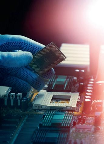
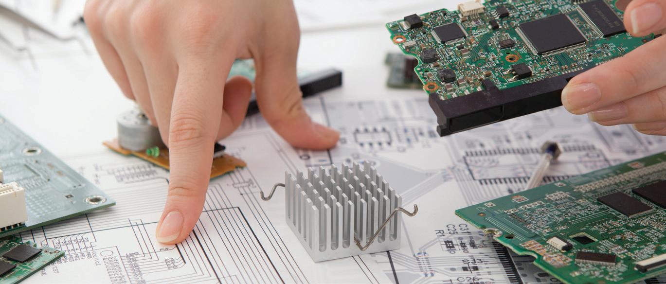
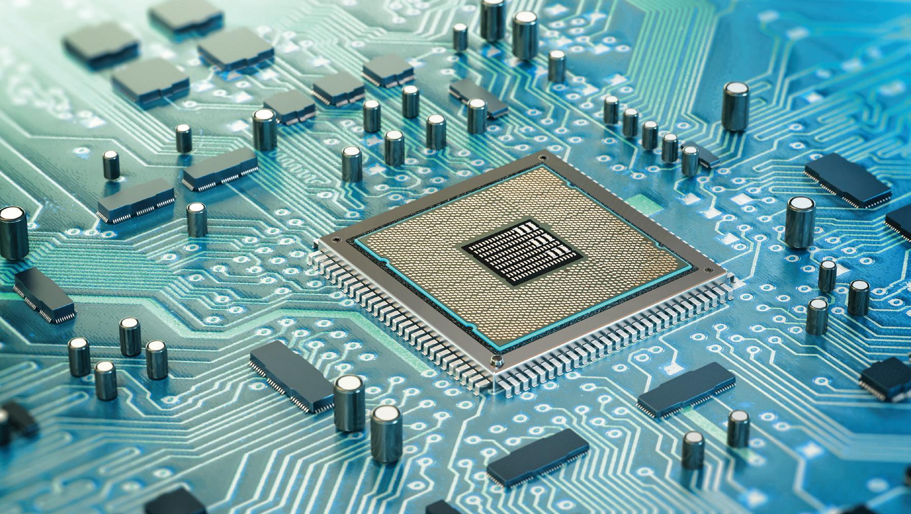
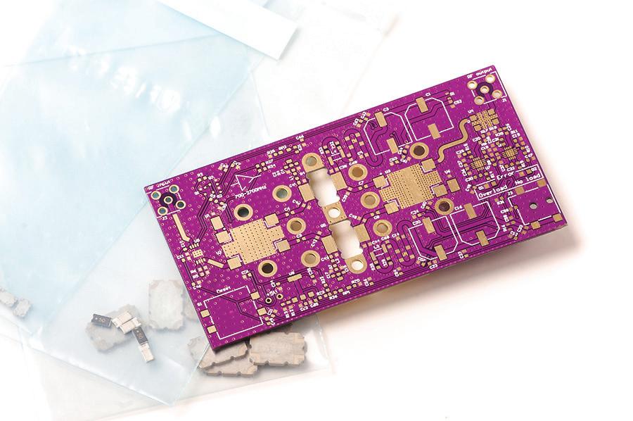
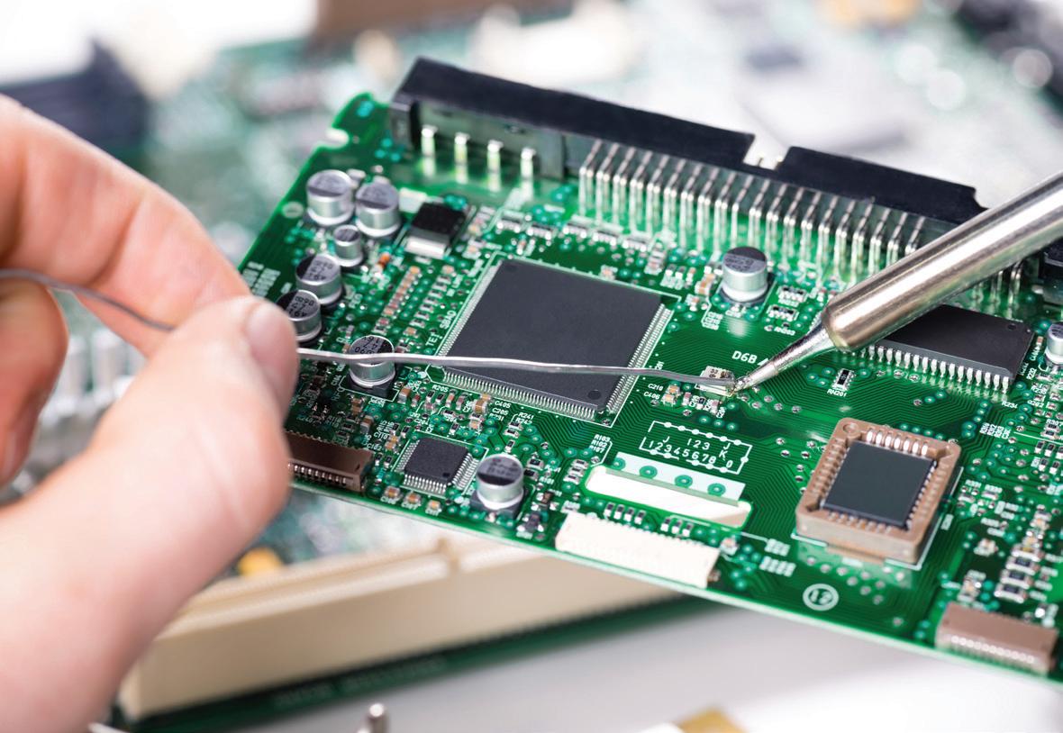
PRINTED CIRCUIT BOARDS (PCBs) ARE ESSENTIAL COMPONENTS IN THE MANUFACTURING OF ELECTRONIC DEVICES. WHILE DESIGNERS OFTEN FOCUS ON THE CIRCUIT LAYOUT AND PICKING THE RIGHT PARTS, ONE KEY DETAIL THAT DOESN’T GET ENOUGH ATTENTION IS THE SURFACE FINISH ON THE PCB. THIS THIN COATING CAN MAKE A BIG DIFFERENCE IN HOW WELL THE BOARD PERFORMS, HOW LONG IT LASTS AND HOW RELIABLE IT IS.
There are plenty of surface finishes to choose from for PCBs, each designed for different conditions, budgets and compatibility needs. This article analyses PCB surface finishes: their types and how to select an appropriate surface finish for various PCBs.
Understanding PCB surface finish
It is important to know what a surface finish actually is and why it matters. Surface finishes are the thin layer of coating that’s applied to copper surfaces on a PCB. Without it, the copper would be exposed to the elements, which would quickly lead to oxidation and corrosion. And this, of course, means the PCB would soon develop catastrophic faults. This finish serves several crucial functions:
Protection: It shields the copper from oxidation and corrosion, ensuring the board’s longevity.
Solderability: It provides a surface suitable for soldering components.
Conductivity: It maintains good electrical conductivity for component connections.
Aesthetics: It can enhance the visual appeal of the PCB. Picking the right finish affects all these things, so it’s a decision worth getting right during manufacturing.
Let’s explore some of the most popular PCB surface finish options available in the market:
1. Hot air solder levelling (HASL)
HASL is a type of finish used on PCBs. The PCB is typically dipped into a bath of molten solder so that all exposed copper surfaces are covered by solder. Excess solder is removed by passing the PCB between hot air knives.
Advantages:
• Excellent solderability: the solder coating improves the ability of components to be soldered to the board.
• HASL-coated boards have a longer shelf life compared to other finishes like OSP.
• HASL is a relatively inexpensive and readily available surface finish.
• It provides a consistent and even layer of solder, promoting reliable solder joints.
Disadvantages:
• Not ideal for fine-pitch components. The unevenness of the HASL finish can be a problem for fine-pitch surface mount technology (SMT) components, making it unsuitable for certain applications.
• Traditional HASL uses a tin–lead alloy, which can be a concern for environmental regulations. Lead-free HASL options are available. Thermal stress: the heat involved in the HASL process can potentially stress the PCB laminate.
• Not suitable for high-frequency applications.
• Not suitable for PTH (Plated Through Hole) components. >
Electroless nickel immersion gold (ENIG) is a type of surface plating used for PCBs. It consists of an electroless nickel plating covered with a thin layer of immersion gold, which protects the nickel from oxidation. This combination provides corrosion resistance, solderability and good electrical properties. ENIG is commonly used to protect copper pads and plated through-holes from oxidation and to facilitate soldering.
Advantages:
• The primary benefits of ENIG are its excellent surface planarity. This makes it particularly suitable for PCBs with finepitch components.
• Robust barrier against oxidation: the nickel layer acts as a barrier to prevent copper from the PCB from oxidising, while the thin layer of gold protects the nickel from oxidation.
• Good for high-frequency applications.
• ENIG is an excellent surface finish for wire bonding applications because it provides a highly conductive surface that is easy to bond to.
• ENIG is suitable for multiple reflow cycles, making it a good choice for applications that require repeated assembly.
• Long shelf life, more than one year in controlled conditions.
Disadvantages:
More expensive than other surface finishes, such as HASL or OSP (organic
solderability preservative). The ENIG process involves the deposition of both nickel and gold layers, which contributes to the increased cost.
• ENIG is susceptible to thermal shock, which can cause the nickel layer to crack and peel. This can lead to poor adhesion and other problems.
• Not good for rework and makes PCB repair difficult.
• Less suitable for high-current applications.
3. Immersion tin
Immersion Tin (ISn) is a metallic finish deposited by a chemical displacement reaction that is applied directly over the basis metal of the circuit board, ie, copper. The ISn protects the underlying copper from oxidation over its intended shelf life. It’s a more affordable option than ENIG and immersion silver, and it is also RoHS-compliant. Due to the way tin and copper interact, they eventually diffuse into one another.
Advantages:
• Good solderability: the tin finish readily wets and solders just like bare copper, unlike HASL or ENIG.
• Flat surface suitable for fine-pitch components.
• More affordable than electroless nickelimmersion gold.
• Preferable for press fit pin insertion.
Disadvantages:
• Shorter shelf life than ENIG due to tin whisker growth.
Potential for copper dissolution during the plating process. Not ideal for multiple reflow cycles/ assembly processes.
• Can lead to tin whiskers.
4. Immersion silver
Immersion silver (IAg) is applied directly to the base metal of a PCB via chemical displacement. It’s a more affordable option than ENIG, and it is also RoHS-compliant. Due to the way copper and silver interact, they eventually diffuse into one another.
Advantages:
• Excellent solderability.
• Good for high-frequency applications.
• Less expensive than immersion gold.
• Flat surface suitable for fine-pitch components.
Disadvantages:
• Prone to oxidation and tarnishing. Requires careful handling and storage. Higher cost compared to HASL. Immersion silver on PCBs typically has a shelf life of six to 12 months under dry storage conditions. After this period, solderability may become a concern.
• When left unprotected from environmental influences, silver reacts with sulfur compounds, like those found in air, to form a black coating of silver sulfide (Ag2S). This reaction is what causes silver to tarnish or become dull. This phenomenon is known as corrosion, and specifically for silver, it’s called tarnishing.
5. Organic solderability preservative (OSP)
An organic, water-based compound, offers OSP a flat finish and is also lead-free. It is an organic coating applied to the copper traces of a PCB to protect them from oxidation and maintain solderability. The OSP finish contains an organic acid that reacts with the copper surface to form a protective layer only a few atoms thick. This prevents air from reaching the copper and oxidising it.
Advantages:
• Appropriate for fine-pitch and BGA PCBs, as compared with HASL, OSP has a small tolerance. Both OSP and ENIG are used for fine-pitch PCB assembly and BGA PCBs.
• In reflow soldering, OSP is removed completely and the bare PCB pads are directly soldered with the SMD components. The soldering effect of OSP PCBs is good.
• OSP is among the cheapest PCB surface finishes.
• OSP is a lead-free finish and does not introduce toxic substances, making it environmentally friendly.
• Good for high-frequency applications.
• Allows good contact resistance for ICT testing.
• Probe pins do not damage soft OSP coating.
Disadvantages:
Limited shelf life: the storage period of OSP PCBs is within three to six months.
• Not suitable for applications requiring multiple reflow cycles.
• Cannot be used for plated-through holes.
• Less robust than metal finishes.
6. Hard gold
A hard gold finish, also known as electrolytic hard gold, is an electroplated gold layer that is thicker and more durable than other finishes like ENIG. It is alloyed with metals such as nickel or cobalt to enhance
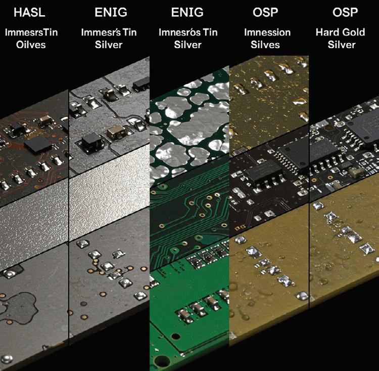
hardness and wear resistance, making it suitable for high-contact areas that require long-lasting electrical connections. Hard gold applications are extremely durable and enjoy a long shelf life. Hard gold is not often used for soldering points, due to poor solderability. It is typically used for edge connectors, battery contacts, test boards and keyboard contacts, all of which require robust, high-wear connections for data transmission and electrical continuity.
Advantages:
• Extremely durable.
• Excellent for applications requiring multiple insertions.
• Very good corrosion resistance.
• RoHS compliant.
• Gold is an excellent conductor, ensuring reliable electrical connections.
Disadvantages: The most expensive option. Overkill for many standard applications.
• Can cause solderability issues if not properly applied.
• Poor solderability performance: hard gold is not easily soldered, making it less suitable for applications requiring solderability.
• Hard gold is not recommended for plated through-holes (PTH).
7. ENEPIG
ENEPIG (electroless nickel, electroless palladium, immersion gold) is a type of PCB surface finish that involves a three-layer coating on the copper pads of a printed circuit board. It consists of a nickel base, followed by a palladium layer, and a top layer of gold, all applied through electroless chemical processes. It is a similar to ENIG, except it adds a palladium layer to the mix. The combination of gold and palladium offers a more cost-effective plating solution than pure gold and is more durable than other finishes.
Advantages:
The palladium layer in ENEPIG enhances wire bonding capabilities more than ENIG, especially for gold and aluminium wire bonding.
• Multiple reflow soldering capability. ENEPIG provides excellent solderability.
• The combination of nickel, palladium and gold provides robust corrosion resistance, protecting the underlying copper from environmental factors such as humidity and chemical exposure.
• ENEPIG-coated PCBs have a long shelf life.
• Lead free and RoHS compliant. Disadvantages:
• ENEPIG is generally more expensive than other surface finishes such as HASL and OSP.
• The ENEPIG process involves multiple steps and requires precise control of plating thickness and uniformity. This complexity can lead to higher production costs and longer lead times compared to simpler surface finishes.
8. EPIG/EPAG
EPIG (electroless palladium immersion gold) and EPAG (electroless palladium autocatalytic gold) are nickel-free PCB surface finishes designed to avoid signal loss from nickel layers, making them ideal for high-frequency RF applications. Both use a palladium base layer topped with gold, but differ in gold deposition methods: EPIG uses immersion gold, resulting in a thinner layer, while EPAG employs autocatalytic gold, allowing for a thicker gold coating. This thicker layer in EPAG supports more demanding uses like gold wire bonding and soldering, making it more versatile. Both finishes are particularly suited for markets requiring non-magnetic bonding such as military, aerospace and deep-sea RF applications.
Advantages (EPIG):
• Nickel-free, which is beneficial for highfrequency applications.
• Suitable for fine-pitch designs and high-density interconnects (HDI) as it eliminates the nickel layer.
• Can be used for both soldering and wire bonding.
• High reliability and uniform thickness.
Disadvantages:
• The immersion gold layer may be thinner compared to autocatalytic gold.
Advantages (EPAG):
• Offers a thicker gold layer, which can be beneficial for applications requiring more robust connections.
• Suitable for wire bonding and soldering.
• Can be used in demanding applications due to its non-magnetic properties.
Advantages:
• The autocatalytic gold process may be more complex and require careful control.
Key Differences:
• Gold thickness: EPAG typically has a thicker gold layer than EPIG.
• Process complexity: EPIG is generally simpler to implement than EPAG.
• Applications: EPAG is often preferred for applications requiring thicker gold layers and more robust connections, while EPIG is suitable for fine-pitch designs and high-frequency applications.
Factors to consider when selecting a PCB surface finish
Application requirements
The primary factor guiding the selection of a PCB surface finish should be the intended application of the PCB. For instance:
• High-frequency applications typically benefit from finishes such as ENIG or immersion silver.
For boards that will undergo multiple reflow cycles, finishes like ENIG or (HASL) may be more suitable.
• In areas subjected to wear, such as edge connectors, a hard gold finish is advisable.
• EPIG without the nickel layer improves signal performance in high-frequency and RF PCB design.
• EPAG and ENEPIG is typically the best option for wire bonding due to its thickness and uniformity.
Component technology
The nature of the components utilised will impact your finish choice:
• Fine-pitch components require a flat surface, making ENIG, immersion tin or OSP ideal options.
• Smooth and durable surface finishes, such as gold or immersion tin, are generally preferred for press-fit connectors.
• Any surface finish is typically compatible with through-hole components.
• Bottom terminated components (BTC) such as BGA and QFN perform optimally with ENIG.
Environmental conditions
It is essential to consider the operational environment of your PCB:
• In high humidity conditions, more corrosion-resistant finishes like ENIG are advisable.
• For applications exposed to extreme temperatures, hard gold and ENIG prove to be the most suitable options due to their superior durability and conductivity. When exposure to chemicals or solvents is anticipated, finishes with high corrosion resistance, like ENIG and hard gold, are preferred.
Shelf-life requirements
For long-term storage of your PCBs, keep in mind the following considerations:
• For a PCB surface finish that offers a prolonged shelf life, both ENEPIG and hard gold are outstanding options.
• ENIG also provides an extended shelf life and is suitable for a variety of applications.
• Alternative choices include immersion silver and HASL.
• It is important to ensure that materials are stored in a humidity-free environment, following established guidelines to achieve optimal results.
OSP and immersion finishes generally have shorter shelf lives, normally not longer than six months.
Regulatory compliance
It is important to keep in mind that different industries will have particular compliance requirements.
• PCB surface finish choices can significantly impact regulatory compliance, primarily concerning RoHS directives and other environmental standards. The type of finish, like HASL, ENIG or OSP, determines its ability to comply with restrictions on heavy metals and other substances. Some finishes, particularly those involving lead, may not be compliant, requiring alternative options.
Selecting the right surface finish for your PCB is a crucial decision that can significantly impact the product’s performance, reliability and cost. By understanding the characteristics of different finishes and carefully considering specific requirements, you can make an informed choice that optimises your PCB for its intended application.
Remember, there’s no one-size-fits-all solution when it comes to PCB surface finishes. Each project may require a different approach, and what works best for one application might not be ideal for another. Stay informed about new developments in surface finish technology, as innovations in this field continue to offer new possibilities for PCB design and manufacturing.
By taking the time to select the best surface finish for your PCB, you’re investing in the quality and longevity of your electronic products. Whether you’re working on a highfrequency communication device, a rugged industrial controller or a cutting-edge medical device, the right surface finish can make all the difference in achieving optimal performance and reliability.

Researchers at Case Western Reserve University have developed an environmentally safer type of plastic that can be used for wearable electronics, sensors and other electrical applications.
The material, a so-called ferroelectric polymer, is made without fluorine, considered a ‘forever’ chemical that hurts the environment because compounds made with it don’t break down quickly or at all.
Although the researchers are still working to improve the material’s electric and elastic properties, the potential is vast for its flexibility of electronic uses and eco-friendly structure.
“How this material generates its electric properties is also fundamentally new,” said lead researcher Lei Zhu, a professor of macromolecular science and engineering at the Case School of Engineering. “Unlike current ferroelectric materials, it doesn’t have to crystallise to lock in the polarity that gives it electrical properties.”
Polymers are large molecules composed of long chains of smaller molecular units that can be man-made — such as plastics — or natural, like in a person’s hair or DNA. Changing a polymer’s molecular structure and length can vary its strength, flexibility, heat-resistance and ability to be recycled.
Ferroelectricity refers to certain materials with what is known as “spontaneous polarisation” that can be reversed by applying an electric field — like an on–off switch. Ferroelectric materials allow for the development of smaller, more efficient electronic devices, reducing reliance on traditional energy sources.
The new material Zhu and his research team have created is both flexible and has what is known as tuneable electronic properties, which means they can be switched on and off.
They have wide applications in infrared detectors and sensors in wearable electronics, for which the materials need to be soft, pliable and elastic to be compatible with the human body. Conventional ceramic ferroelectric materials are rigid and brittle.
Polymers have the advantage of being flexible and lightweight, but the dominant ferroelectric polymer, poly(vinylidene fluoride), or PVDF, doesn’t naturally degrade in the environment, making it a ‘forever chemical’. The new material is made without fluorine.
Ferroelectric polymers also have applications in sensors for ultrasound diagnostic tools because they are acoustically compatible with biological tissues. They are also potentially useful in augmented and virtual reality (AR and VR) goggles.
“We’re still in the development stage of synthesising small quantities and investigating the properties. But we’re excited about the potential to replace environmentally harmful plastics in sensors and detectors,” Zhu said.
The research explaining the discovery has been published in the journal Science. The new material is patent pending.
Monash University is developing and deploying MAVERIC, in collaboration with NVIDIA, Dell Technologies and the CDC Data Centres (CDC). The advanced AI supercomputer will use technology to solve complex problems across a vast span of human endeavours.
Monash University Vice-Chancellor and President Professor Sharon Pickering said the collaboration with leading technology partners is essential in bringing together the expertise needed to strengthen sovereign capabilities right across the research and development pipeline.
Our focus is on solving real problems and putting AI to work in a meaningful way — from breakthroughs in cancer detection, to redefining what’s possible in preserving the health of our planet for future generations,” Pickering said.
Featuring the NVIDIA GB200 NVL72 platform, MAVERIC will be purpose-built for large-scale AI and data-intensive workloads.
Monash will deploy the NVIDIA GB200 NVL72 architecture through Dell Technologies, which integrates NVIDIA accelerated computing, NVIDIA AI Enterprise software and AI frameworks into its high-performance Dell Integrated Rack Scalable Systems (IRSS), Dell’s engineering expertise and integrated solutions will give Monash a robust and efficient platform tailored for AI research at scale, forming a critical foundation for MAVERIC’s advanced computing capabilities.
MAVERIC’s AI capabilities, run on Dell AI Factory with NVIDIA, will allow the university to participate in the fight against some of humanity’s biggest challenges, including disease and environmental science. To do so while boosting Australia’s sovereign AI capabilities is a win for the research community and a win for Australia,” said Angela Fox, SVP and Managing Director ANZ, Dell Technologies.
CDC, a leading developer, owner and operator of secure and connected large-scale data centres in Australia and New Zealand, will house MAVERIC at its data centre in Brooklyn, Melbourne. The GB200 NVL72’s closed-loop liquid-cooling design delivers up to 300× greater water efficiency than traditional air-cooled systems, enabling heat removal without consumptive water use. CDC data centres are designed to operate with no water consumption for primary cooling, which helps save billions of litres of water annually across CDC’S campuses.
Work to build MAVERIC will commence in 2025 with the platform to be activated in early 2026.


Aqueous batteries are safe and relatively low-cost, but their adoption in new energy storage systems — such as grid storage and electric vehicles — is limited due to material compatibility. Many electrode materials do not perform well in aqueous electrolytes. For organic redox polymers in particular, hydrophobicity has been a barrier.
Now, researchers from Tohoku University have developed a new organic redox polymer that addresses these challenges. To overcome the hurdles, the researchers introduced p-dihydroxybenzene — an organic molecule with high charge storage capacity — into a polyamine, which is water-soluble due to its positive charge. This was achieved through a simple condensation reaction.
The resulting polymer retains high hydrophilicity, can be used as an electrode-active material at room temperature (25°C) and can be broken down into its raw components under mild conditions at temperatures below 100°C.
“This study provides a design strategy for making hydrophobic redox molecules compatible with aqueous systems. By combining high charge storage capacity with recyclability, we can open new directions for sustainable battery research,” said Kouki Oka, associate professor at Tohoku University.
The research findings highlight two key benefits; the use of water-based electrolytes avoids the risk of fire associated with conventional flammable solvents. Second, because the new polymers are made from abundant elements and can be easily decomposed, they may help reduce resource consumption and plastic pollution.


RESEARCHERS AT THE UNIVERSITY OF CALIFORNIA SAN DIEGO HAVE DEVELOPED A SIMPLE METHOD TO CHARACTERISE LITHIUM METAL BATTERY PERFORMANCE WITH THE HELP OF SCANNING ELECTRON MICROSCOPY. THE ADVANCE COULD ACCELERATE THE DEVELOPMENT OF SAFER, LONGER-LASTING BATTERIES FOR ELECTRIC VEHICLES AND GRID-SCALE ENERGY STORAGE.
Lithium metal batteries have the potential to store twice as much energy as today’s lithium-ion batteries. That could double the range of electric cars and extend the runtime of laptops and phones. But to realise this potential, researchers must tackle a longstanding challenge: controlling lithium morphology, or how lithium deposits on the electrodes during charging and discharging.
When lithium deposits more uniformly, the battery can achieve longer cycle lifetimes. By contrast, when lithium deposits unevenly, it forms needle-like structures known as dendrites that can pierce a battery’s separator and cause the battery to short-circuit and fail.
Historically, researchers have largely determined the uniformity of lithium deposits by visually assessing microscope images. This practice has led to inconsistent analyses between labs, which has made it difficult to compare results across studies.
“What one battery group may define as uniform might be different from another group’s definition,” said study first author
Jenny Nicolas, a materials science and engineering PhD candidate at the UC San Diego Jacobs School of Engineering. “The battery literature also uses so many different qualitative words to describe lithium morphology — words like chunky, mossy, whisker-like and globular, for example. We saw a need to create a common language to define and measure lithium uniformity.”
To do so, Nicolas and colleagues developed a simple algorithm that analyses how evenly lithium is spread across scanning electron microscopy (SEM) images. The researchers used SEM because it offers detailed images of battery electrodes by capturing 3D surface features as 2D grayscale images — it is also a widely used technique in battery research.
To use their method, the team first takes SEM images of battery electrodes and converts them to black and white pixels. The white pixels represent the topmost lithium deposits in the sample and black pixels represent either the substrate or inactive lithium. The images are divided into multiple regions, and the algorithm counts the number

of white pixels in each, then calculates a metric called the index of dispersion (ID).
“The index of dispersion is a measure of lithium uniformity,” Nicolas said. “The closer it is to zero, the more uniform the lithium deposits. A higher value means less uniformity and more clustering of lithium particles in certain areas.”
The team first validated the method on 2048 synthetic SEM images with known particle size distributions. The ID measurements aligned with the ground-truth distributions, which confirmed the method’s accuracy. The team then applied the method to real electrode images to analyse how lithium morphology changes over time under different cycling conditions. They found that as batteries cycled, the ID increased — indicating more uneven lithium deposits. Meanwhile, the energy required for lithium to deposit increased — a sign of degradation. In addition, the researchers found that local peaks and dips in the ID consistently appeared just before cells failed. Such peaks and dips could serve as an early warning sign of short circuits.
A big advantage of this method is that it is accessible. Battery researchers already use SEM imaging as part of their studies, Nicolas noted, and they can use the simple algorithm presented here to calculate the ID from the data they already collect.
“Our tool can be employed as a low-hanging fruit for researchers to take their analysis to the next level by utilising image analysis to its fullest potential,” Nicolas said.
The research findings were published in Proceedings of the National Academy of Sciences.
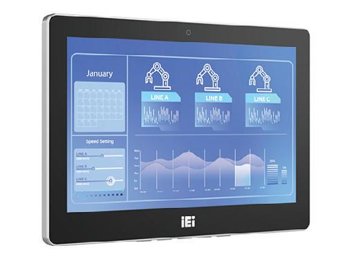
ICP Electronics Australia introduces iEi’s industrial display solutions with the DM2 Series — a comprehensive line of industrial touch monitors built for applications such as factory automation, transportation hubs, kiosks and more. With screen sizes ranging from 10.1″ to 23.8″, including square, widescreen and ultra-wide formats, the series of industrial monitors offers flexibility for diverse installation needs.

Each monitor features a high-brightness display (up to 1000 nits) with anti-glare and anti-UV PCAP touchscreens, for clear visibility in bright or outdoor environments. The rugged design also features an IP65-rated front panel for protection against dust and water. The entire unit supports a wide operating temperature range of -20 to 60°C.
Optional features such as a built-in 720p camera, dual 2 W speakers and an integrated USB hub enhance user interaction and system integration. With multiple mounting options and frontaccessible OSD buttons, installation and adjustments are made simple and accessible.
Whether upgrading an existing industrial HMI set-up or building a new interactive system from the ground up, the IEI DM2 Series offers a versatile, rugged and future-ready solution.
ICP ELECTRONICS AUSTRALIA www.icp-australia.com.au
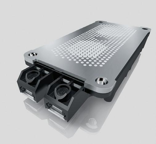
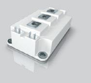
Power module manufacturer Semikron Danfoss offers a range of modules with pre-applied thermal interface materials (TIM).
A thermal interface material is a substance inserted between a heat-generating component and a heat-dissipating device, such as a heat sink, to improve thermal coupling by filling microscopic gaps and facilitating heat transfer. TIMs enhance heat dissipation, preventing overheating by replacing insulating air with conductive material.
In power electronics systems design, the thermal interface material (TIM) plays a crucial role in the end product. It is the main contributor to the complete thermal impedance between the power electronic chip and the heat sink.
Semikron Danfoss offers more than 30 million pre-printed modules, including thermal grease or phase change materials depending on customer requirements (eg, performance increase, reduced handling effort) and module type (with or without baseplate).
SEMIKRON DANFOSS www.semikron.com.au

AN INTERNATIONAL TEAM LED BY RESEARCHERS FROM UNIVERSITY COLLEGE LONDON HAS DEVELOPED DURABLE NEW SOLAR CELLS CAPABLE OF EFFICIENTLY HARVESTING ENERGY FROM INDOOR LIGHT, MEANING DEVICES SUCH AS KEYBOARDS, REMOTE CONTROLS, ALARMS AND SENSORS COULD SOON BE BATTERY FREE.
The team used a material called perovskite, which is increasingly used in outdoor solar panels and, unlike traditional silicon-based solar panels, has potential to be used indoors as well, as its composition can be adjusted to better absorb the specific wavelengths of indoor light.
A major drawback of perovskite, however, is that it contains tiny defects in its crystal structure — known as ‘traps’ — which can cause electrons to get stuck before their energy can be harnessed. These defects not only interrupt the flow of electricity but also contribute to the material’s degradation over time.
In a study published in the journal Advanced Functional Materials, the team describes how they used a combination of chemicals to reduce these defects, potentially making perovskite indoor solar panels viable.
The perovskite photovoltaics they engineered, the team say, are about six times more efficient than the best commercially available indoor solar cells. They are more durable than other perovskite devices and could be used for an estimated five years or more, rather than just a few weeks or months.
Senior author Dr Mojtaba Abdi Jalebi, Associate Professor at the UCL Institute
for Materials Discovery, said: “Billions of devices that require small amounts of energy rely on battery replacements — an unsustainable practice. This number will grow as the Internet of Things expands. Currently, solar cells capturing energy from indoor light are expensive and inefficient. Our specially engineered perovskite indoor solar cell can harvest much more energy than commercial cells and is more durable than other prototypes. It paves the way for electronics powered by the ambient light already present in our lives.
“We are currently in discussions with industry partners to explore scale-up strategies and commercial deployment. The advantage of perovskite solar cells in particular is that they are low-cost — they use materials that are abundant on Earth and require only simple processing. They can be printed in the same way as a newspaper.”
One problem in earlier perovskite solar cells was the presence of a high density of traps in the material and its interfaces with charge collecting layers, which disrupted the flow of charge and caused energy to be lost as heat.
The research team introduced a chemical (rubidium chloride) that encouraged a more homogeneous growth of perovskite crystals with minimal strains, reducing the density of these traps.
Two other chemicals — organic ammonium salts N,Ndimethyloctylammonium iodide (DMOAI) and phenethylammonium chloride (PEACl) — were added to stabilise two types of ions (iodide and bromide ions), preventing them from migrating apart and bunching into different phases, which degrades the performance of the solar cell over time, again by disrupting the flow of charge through the material.
Lead author Siming Huang, a PhD student at UCL’s Institute for Materials Discovery, said: “The solar cell with these tiny defects
is like a cake cut into pieces. Through a combination of strategies, we have put this cake back together again, allowing the charge to pass through it more easily. The three ingredients we added had a synergistic effect, producing a combined effect greater than the sum of the parts.”
The team found that their solar cells converted 37.6% of indoor light (at 1000 lux — equivalent to a well-lit office) into electricity, a record for this type of solar cell optimised for indoor light, that is with a bandgap of 1.75 eV (electron volts).
The researchers also tested the
solar cells to see how well they resisted degradation over time.
After more than 100 days, the newly engineered cells retained 92% of their performance, compared to a control device (perovskite whose flaws had not been reduced) that retained only 76% of its initial performance.
In a harsh test of 300 hours of continuous intense light at 55°C, the new solar cells retained 76% of their performance, while the control device dropped to 47%.
The team involved researchers from the UK, China and Switzerland.
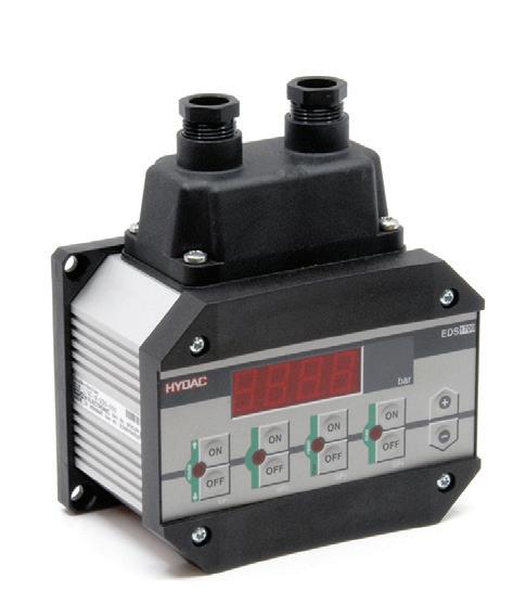
The HYDAC EDS 1700 is a high-performance electronic pressure switch designed for precise operation in hydraulic and pneumatic applications. Featuring an integrated pressure measurement cell, a clear four-digit display and four independent switching outputs, it allows operators to control and monitor system pressure. Each switching and switch-back point can be set independently via the intuitive keypad, making adjustments quick and easy while reducing downtime.
Advantech has introduced the EPC-R7300 Orin Nano Super, an ultracompact embedded AI Box PC powered by the NVIDIA Jetson Orin Nano 8GB module. Delivering up to 67 TOPS of AI performance with just 25 watts of power consumption, this Ubuntu-ready system is optimised for small large language models (LLMs), vision-language models (VLMs) and vision transformers (ViTs) in edge AI applications.

Paired with JetPack 6.2, the AI box PC supports AI models with fewer than 10 billion parameters, enabling natural language processing, robotics, voice interfaces, retail analytics and industrial vision. It provides a high-performance, privacy-focused platform for real-time intelligence across industries.
For enhanced system integration, the electronic pressure switch offers a selectable analog output in either 4–20 mA or 0–10 V, enabling direct connection to PLCs and monitoring systems. Built with an integrated strain-gauge sensor on a stainless steel membrane, the unit delivers measurement accuracy between 0.5% and 1% of full scale, enabling stable and repeatable performance over millions of switching cycles.
The pressure connection and display/keypad module can be rotated through 180°, allowing for top or bottom mounting to suit different installation layouts. The display can also be configured to show pressure readings in bar, psi, or alternative units such as kN or kg, catering to a range of applications.
Users can also set relay functions as normally open or normally closed, program switch-on and switch-off delays from 0 to 90 s, apply hysteresis and view peak pressure values. For additional security, programming menus can be hidden to prevent unauthorised changes.
The HYDAC EDS 1700 is an innovative solution for critical pressure monitoring and control. Whether in fixed industrial systems or high-cycle operations, it is designed to provide the precision and functionality needed to keep processes running smoothly.
HYDAC INTERNATIONAL www.hydac.com.au
Designed for developers, the PC features RS-485, CANbus, multiple Ethernet ports and support for USB/IP cameras. It includes 2 x USB 3.2, HDMI 2.0 (4K output) and 3 x M.2 slots for Wi-Fi 6, 4G/5G and NVMe SSD storage. The PC can also be integrated with NVIDIA’s ecosystem, for hassle-free deployment. With a rugged design, the device supports -2060ºC temperatures, 936 V power input and 3.0 Grms vibration tolerance, making it suitable for harsh industrial environments. Up to five rear I/O configurations, including serial ports, isolated DIOs, USB 2.0 and a 4-port GbE hub, enable extensive customisation. With built-in BSP drivers, the EPC-R7300 facilitates seamless functionality for next-gen edge AI applications.
ADVANTECH AUSTRALIA PTY LTD www.advantech.net.au
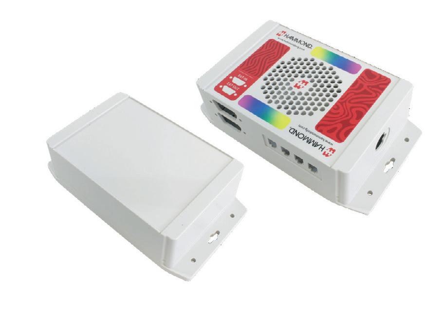
Hammond Electronics has added reduced height sizes to its IP68 sealed, UL listed 1554, 1555 and 1555F polycarbonate enclosures.
The 1554 and 1555 UL listed polycarbonate enclosure families offer IP68 (NEMA Type 4, 4X, 6, 6P, 12 and 13) environmental sealing and an IK08 impact rating. A further 10 sizes of shallow enclosures have also been added: the F, 120 x 90 mm; the N, 120 x 120 mm, and the R, 160 x 160 mm are available with heights of 45 and 61 mm.
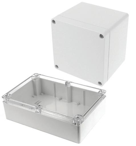


The U size, 200 x 120 mm, is available in heights of 17 and 42 mm. All 1554 and 1555 plan sizes are available with plain, styled, clear and smoked lids. The 1555F range has a flanged lid to facilitate surface mounting and the base is styled to accept membrane keypads and other components.
The enclosures come with optical 1.6 mm galvanised steel panels for all sizes for mounting heavier components. Internal DIN rail mounting tabs are also moulded into most sizes, with vertical PCB guides in all but the smallest A and B sizes. The enclosures also feature M3 threaded brass inserts and/or standoffs for PCB or inner panel mounting in all but the smallest B size.
HAMMOND ELECTRONICS PTY LTD www.hammfg.com
The FAULHABER IERF3 L incremental encoder is designed to provide precision in spaceconstrained applications. Built on an advanced optical sensing platform, the IERF3 L delivers optimised resolution, 0.1° positioning accuracy and 0.007° repeatability — making it suitable for high-precision motion control.
Available in 22, 32 and 42 mm diameters, the encoder is matched to FAULHABER’s BXT series of brushless flat DC micromotors. It features a built-in line driver for noise-resistant, long-distance signal transmission, and can be optionally paired with a brake for added control.
The encoder is built for demanding environments like metrology, robotics, microscopy and semiconductor manufacturing, where precision and reliability are paramount. As an optical encoder, it is also immune to magnetic interference — an added advantage in sensitive installations.
The IERF3 L incremental encoder is designed for applications that call for tight tolerances and optimised feedback.
ERNTEC PTY LTD www.erntec.net
Format: 180 x 135 mm
METCASE’s UNICASE instrument enclosures are now available in traffic white (RAL 9016) as standard, complementing the existing light grey (RAL 7035) and black (RAL 9005) options. Custom colours are also available on request.
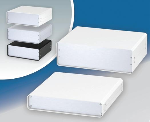
UNICASE is suitable for a range of applications including measuring and control, feedback control, peripheral devices and interfaces, switchboxes, modems, medical and laboratory technology.
These aluminium enclosures can be assembled and disassembled quickly and easily — speeding up installations, inspection and maintenance. Removing the U-shaped top allows rapid access to the electronics.
PCBs slide in and out of guide rails in the chassis/assembly extrusions. Anodised front and rear panels are supplied (along with four push-in non-slip rubber feet for the base). The front panel is recessed to protect controls.
METCASE manufactures UNICASE in 10 standard sizes from 185 x 180 x 65 mm to 250 x 300 x 50 mm.
Accessories include PCB fixing screws and a white polyamide (PA 2200) assembly tool that locates the blue threaded nut holders in the extrusion profiles, aligning them with the top and base cover screws for faster installation.
METCASE can also supply UNICASE fully customised. Services include custom sizes (heights, widths and depths), custom front panels, CNC machining, fixings and inserts, painting and finishing, and photo-quality digital printing of legends, logos and graphics.
ROLEC OKW AUSTRALIA NEW ZEALAND P/L www.metcase.com.au


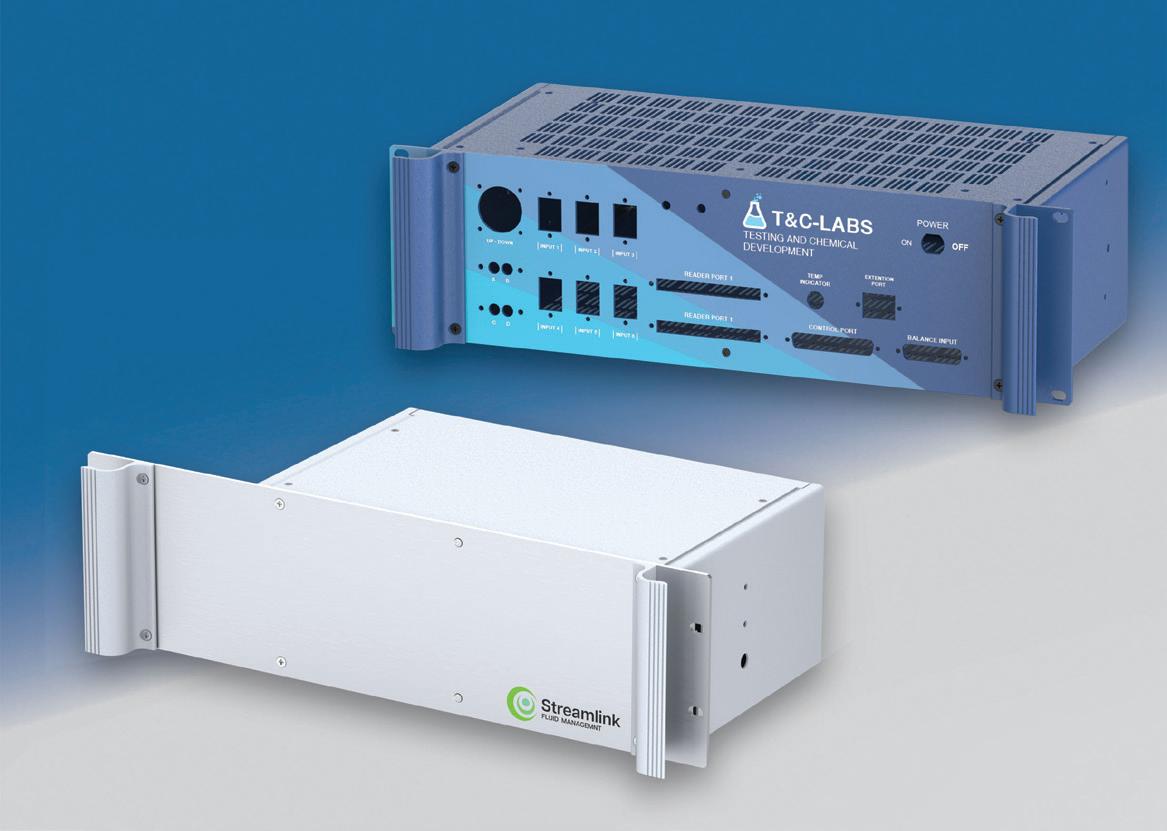
These cases are suitable for wallmounted racks, where space constraints and weight considerations call for a compact and lightweight solution. These features make them perfect for applications in health care, retail or edge computing where space can be limited.
Shallow 19 ″ rack cases offer space-saving installation and optimised airflow
Shallow-depth rack cases are smaller and weigh less, so they’re significantly easier to handle and install — an essential feature for applications where space inside the rack is at a premium.
Devices designed to operate in shallowdepth rack cases typically generate less heat compared with larger, more power-intensive equipment. This makes cooling less complex and more efficient.
Shallow-depth case applications in automation typically include programmable logic controllers (PLCs), motor controllers and remote input/output (I/O) modules for data acquisition and control. For networking and communications, the cases are specified for switches, IoT/IIoT gateways and fibre-optic distribution units.
In test and measurement, shallow cases can be used to house data logging, signal generation or spectrum analysis devices.
THERE IS AN INCREASING INTEREST IN SHALLOW-DEPTH AND OFFSET/ASYMMETRICAL CASES FOR 19″ RACK ELECTRONICS. THEY’RE BECOMING MORE POPULAR FOR A WIDE RANGE OF APPLICATIONS — FITTING NEATLY INTO SPACES WHERE DEEPER OR CONVENTIONAL SYMMETRICAL ENCLOSURES WOULD BE IMPRACTICAL OR IMPOSSIBLE TO USE.
These cases are also specified for A/V and broadcasting applications such as digital signal processors, video switchers, stage lighting/digital multiplex (DMX) controllers, portable recording equipment and rack-mounted computers for editing and playback.
Shallow cases are also used to house medical imaging equipment (ultrasound or portable X-ray machines) and diagnostics instrumentation in laboratories or mobile healthcare units. They also find favour with the military for radar control units and communications relay systems in field deployments.
They’re often used in outside broadcast vans that require a compact yet robust housing for video switchers, recording
equipment or communications systems. Meanwhile, the retail sector specifies shallow cases for point of sale and for driving digital signage displays.
Offset cases help electronics designers to squeeze more space out of racks when a functional, spatial or ergonomic requirement makes a symmetrical design impractical. These configurations provide flexibility for installations where standard layouts cannot accommodate the specific equipment or cabling needs.
Some components (power supplies or fan modules) may be deeper than others (network switches or patch panels). An
supplies can be positioned closer to the centre of the rack for stability, while lighter equipment occupies the offset portion.
In test/measurement or military applications, equipment can often be modular or non-standard in size. Asymmetrical cases allow for bespoke configurations, such as housing a control interface or display on the shallow side while reserving the deeper side for processing units or power systems.
Shallow-depth rack cases are smaller and weigh less, so they’re easier to handle and install.
offset design allows one side of the rack to house deeper components while keeping the other side shallower to save space.
These cases are also a great choice when there’s a need for increased space on one side of the rack for routing and organising cables. In networking applications, one side may house shallow devices such as patch panels, while the other side accommodates cable bundles or cable-management trays.
Asymmetrical designs can also be used to optimise weight distribution, particularly for portable or mobile applications. Heavier components such as amplifiers or power
For thermal management, offset cases can direct airflow across specific components with higher cooling demands while leaving other sections vented or sealed as needed. This is common in telecommunications or industrial automation where some components generate more heat than others.
Offset cases are sometimes chosen to enhance accessibility or aesthetics. For example, front-facing displays or controls might be positioned in the shallow section, while deeper components are hidden or mounted further back for a clean and ergonomic layout.
Which 19 ″ rack cases are suitable for shallow and offset designs?
Metcase offers four 19″ rack cases: COMBIMET, VERSAMET, UNIMET and METTEC — all of which can be supplied in shallow depths on request. For offset designs, COMBIMET is the recommended housing. Further customising options
In addition to custom depths and offset designs, modification options for Metcase 19″ rack cases also include:
• Custom front panels
CNC machining — punching, folding, milling, drilling and tapping
• Fixings and inserts
• Custom colours (powder coating, wet painting)
• Photo-quality digital printing of legends, logos and graphics.
All customisation work is carried out in-house to save time, money and administration. It’s also better for the environment because the enclosures don’t have to be shipped between multiple suppliers.
Metcase offers advice on the best standard or customised enclosures for a range of rack-mounted electronics.

We are pleased to announce that ONBoard Solutions, a valued longterm member of our organisation, has recently become a Sponsor Member! Their continued support reflects a strong commitment to our industry and the work we do together. We look forward to building on this long-standing relationship through their sponsorship.
ONBoard Solutions is a 100% Australianowned company with over 20 years of industry experience in suppling critical products and services to sectors where precision and reliability are essential, including electronics, medical devices, renewable energy, semiconductor, and defence.
Their core offerings include the production of custom-engineered automation equipment, a comprehensive range of cleanroom and GMP supplies, and specialised material technologies, including adhesives, solders, coatings, and cleaning solutions, designed to meet compliance standards and optimise performance.
ONBoard Solutions’ services extend beyond supply, providing consulting on ISO class compatibility, cleanroom requirements, and equipment selection, training in ISO gowning and cleanroom practices, and full engineering support from automation design through to integration and ongoing technical assistance. Their credentials include ISO 9001 accredited quality management systems, exclusive distribution rights for MBTech Cleaning Systems and Practical Components in Australia and New Zealand, and a strong network of global partners and clients. With this combination of technical expertise, comprehensive products, and engineering support, ONBoard Solutions provides a complete and reliable framework for highprecision industries.


Recognizing the need to redefine its role in response to global shifts in the electronics manufacturing sector, IPC rebranded as the Global Electronics Association earlier in 2025. This new identity reflects the organisation’s broader perspective, moving beyond its U.S. origins to embrace its place in the wider international market, of which the U.S. industry is only one part. While continuing to develop and update the IPC suite of standards and certification programs, the Global Electronics Association is now focusing at a corporate level on the complex, interconnected supply chains that underpin the industry. Recently, it has drawn attention to the effects of copper tariffs on U.S. electronics manufacturers and the urgent need for the EU to strengthen the resilience of its own electronics manufacturing industry. It is also prioritising the development of skilled workforces in regions where economic conditions now favour local manufacture.
The SMCBA is proud to mark 30 years of membership with the Global Electronics Association and actively supports its programs and objectives.
SMTA Silicon Valley and SMCBA Joint Webinar “Backward Compatible Assembly and Reliability”
Multiple Presentations:
• Dave Hillman “Lead-free BGAs and a Tin-Lead SMT Reflow Process”
• Jasbir Bath “Challenges in Assembly of Tin-Lead Paste with Lead-free BGAs”
• Richard Coyle “Thermal Fatigue Reliability of Backwward Compatible, Mixed Metallurgy BGA Assemblies” 11:00 – 12:30 AEDT October 9 – FREE for SMCBA Members!
FOR ABSTRACTS, BIOS AND BOOKINGS
SCAN QR CODE
Melbourne 20th – 24th October 2025
Sydney 27th – 31st October 2025
EMC Technologies is a leader in EMC testing in Australia and New Zealand and has been hosting Keith Armstrong’s training courses for the last 25 years. Keith is a practicing EMC & electronic design consultant, and wellknown worldwide as an articulate and lively presenter.
In 2000, EMC Technologies invited Keith Armstrong from the UK to teach the first courses on electronic design for compliance with EMC and Safety regulations. These
courses have been held nearly every year since then for the benefit of manufacturers in Australia and New Zealand.

The courses are well received, with a few of the comments from past attendees as follows:
“By the way — just had XXXX in with their latest project. Their design chap was extolling your virtues. It passed first time — no remedial action required — virtually noise floor
Advantech has launched the MIC-743, a powerful edge AI platform designed to bring server-grade AI performance to applications such as video language models (VLMs) and large language models (LLMs).
emissions — and it included Ethernet, PoE, USB and DSP! What more can I say!”
“You have the most comprehensive work in my opinion for a practical EMC engineer or tech, instead of academic based information with no relationship to practice.”
“I would also like to thank you for the interesting and informative course that you presented. I have already begun to implement some design changes in an ongoing project.”
“All participants were very experienced yet I’m sure that the others found it as valuable as I did.”
This year Keith will share the teaching with his Associates, all experts and excellent speakers. The material has been updated; and — because of AUKUS — a full day on Military EMC Testing has been added.
There is also half a day of Live EMC demonstrations, showing how to use low-cost EMC test gear on unshielded testbenches or in the field, to troubleshoot causes of EMC test failure.
For more details, download the complete brochure and registration form from https://www.emctech.com.au/keitharmstrong-emc-2025.

EMC Technologies Pty Ltd www.emctech.com.au

Powered by the NVIDIA Jetson Thor T5000 module, the edge AI platform delivers up to 2070 FP4 TFLOPs of AI performance, enabling real-time inferencing for complex edge applications. Featuring 2560 CUDA cores and 96 Tensor cores, it provides massive computing power for deep learning, computer vision and multimodal AI workloads.
With 128 GB LPDDR5X memory, the platform provides ample bandwidth and capacity to handle large AI models, supporting advanced inferencing tasks such as VLM, LLM and intelligent video analytics without bottlenecks.
Together, these features make the platform suitable for simultaneous multimodal AI processing, empowering edge deployments to run sophisticated AI tasks at scale.
Engineered with a compact, industrial-grade form factor and rich I/O connectivity, the edge AI platform is suitable for diverse deployment environments, including factories, research labs and development centres. Its flexible design enables easy integration with sensors, cameras and peripheral devices, giving developers and system integrators the tools to build end-toend AI solutions faster and with reduced deployment time.
By combining high performance with flexible deployment options, the edge AI platform enables businesses to accelerate innovation and unlock new opportunities in intelligent edge applications. From powering VLM-driven video analytics to running next-generation LLMs, the MIC-743 delivers a stable, scalable foundation for advanced front-end AI workloads.
ADVANTECH AUSTRALIA PTY LTD
www.advantech.net.au
A TEAM OF MATERIALS SCIENTISTS AT RICE UNIVERSITY HAS DEVELOPED A NEW WAY TO GROW ULTRATHIN SEMICONDUCTORS DIRECTLY ONTO ELECTRONIC COMPONENTS.
The method, described in a study published in ACS Applied Electronic Materials, could help streamline the integration of two-dimensional materials into next-generation electronics, neuromorphic computing and other technologies demanding ultrathin high-speed semiconductors.
The researchers used chemical vapour deposition (CVD) to grow tungsten diselenide, a 2D semiconductor, directly onto patterned gold electrodes. They next demonstrated the approach by building a functional, proof-of-concept transistor. Unlike conventional techniques that require transferring fragile 2D films from one surface to another, the Rice team’s method eliminates the transfer process entirely.
“This is the first demonstration of a transfer-free method to grow 2D devices,” said Sathvik Ajay Iyengar, a doctoral student at Rice and a first author on the study along with Rice doctoral alumnus Lucas Sassi. “This is a solid step toward reducing processing temperatures and making a transfer-free, 2D semiconductorintegration process possible.”
The discovery began with an unexpected observation during a routine experiment.
“We received a sample from a collaborator that had gold markers patterned on it,” Sassi said. “During CVD growth, the 2D material unexpectedly formed predominantly on the gold surface. This surprising result sparked the idea that by deliberately patterning metal contacts, we might be able to guide the growth of 2D semiconductors directly across them.”
Semiconductors are foundational to modern computing, and as the industry races towards smaller, faster and more efficient components, integrating higher-performance, atomically thin materials like tungsten diselenide is a growing priority.
Conventional device fabrication requires growing the 2D semiconductor separately, usually at very high temperatures, then transferring it using a series of steps. While 2D materials promise to outperform silicon in certain metrics, turning their lab-scale promise into industry-relevant applications has proven difficult — in large part due to the fragility of the materials during the transfer process.
“The transfer process can degrade the material and damage its performance,” said Iyengar, who is part of Pulickel Ajayan’s research group at Rice.
The Rice team optimised the precursor materials to lower the synthesis temperature of the 2D semiconductor and showed that it grows in a controlled, directional manner.
“Understanding how these 2D semiconductors interact with metals, especially when grown in situ, is really valuable for future device fabrication and scalability,” said Ajayan, Rice’s Benjamin M. and Mary Greenwood Anderson Professor of Engineering.
Using advanced imaging and chemical analysis tools, the team confirmed the method preserves the integrity of the metal contacts, which are vulnerable to damage at high temperatures.
“A lot of our work in this project was focused on proving that the materials system is still intact,” Iyengar said. “We are well-equipped here at Rice to study the chemistry that goes on in this process to a very

fine degree. Seeing what happens at the interface between these materials was a great motivator for the research.”
The success of the method lies in the strong interaction between the metal and the 2D material during growth, Sassi noted.
“The absence of reliable, transfer-free methods for growing 2D semiconductors has been a major barrier to their integration into practical electronics,” Sassi said. “This work could unlock
Unlike conventional techniques that require transferring fragile 2D films from one surface to another, the Rice team’s method eliminates the transfer process entirely.
new opportunities for using atomically thin materials in nextgeneration transistors, solar cells and other electronic technologies.”
In addition to challenges with the fabrication process, another key hurdle in 2D semiconductor design is electrical contacts’ quality, which entails not just low energy barriers but also stable and enduring performance, scalability and compatibility with a wide range of materials.
“An in-situ growth approach allows us to combine several strategies for achieving improved contact quality simultaneously,” said Anand Puthirath, a co-corresponding author of the study.
The project was sparked by a question raised during a US–India research initiative: Could a semiconductor fabrication process for 2D materials be developed on a limited budget?
“This started through our collaboration with partners in India,” said Iyengar, who is the inaugural recipient of the Quad Fellowship, a program launched by the governments of the US, India, Australia and Japan to support early career scientists in exploring how science, policy and diplomacy intersect on the global stage. “It showed how international partnerships can help identify practical constraints and inspire new approaches that work across global research environments.”
Together with a couple of his peers in the Quad Fellowship cohort, Iyengar co-authored an article advocating for “the need for expertise at the intersection of STEM and diplomacy”.
“Greater engagement between scientists and policymakers is critical to ensure that scientific advancements translate into actionable policies that benefit society as a whole,” Iyengar said. “Materials science is one of the areas of research where international collaboration could prove invaluable, especially given constraints such as the limited supply of critical minerals and supply chain disruptions.”


A NEW REVIEW FROM THE UNIVERSITY OF CALIFORNIA, RIVERSIDE, PUBLISHED IN NANO ENERGY, EXPLAINS WHY SOLID-STATE BATTERIES ARE POISED TO TRANSFORM EVERYTHING FROM ELECTRIC CARS TO CONSUMER ELECTRONICS, AND REPRESENTS A MAJOR LEAP IN ENERGY STORAGE.
These batteries replace the flammable liquid found in standard versions with a solid material that is safer and far more efficient. Where today’s batteries may take 30 to 45 minutes to reach 80% charge, solid-state models can cut that time to 12 minutes, and in some cases, as little as three.
Lead author Cengiz Ozkan, a professor of mechanical engineering at UCR, said the benefits come down to chemistry and engineering. “By removing the liquid and using stable solid materials instead, we can safely push more electricity into the battery at once, without the risks of overheating or fires,” Ozkan said.
Conventional lithium-ion batteries move lithium ions, the particles that carry electric charge, through a liquid. But that liquid can degrade over time, limit charging speed and pose fire risks. Solid-state batteries use a solid material instead, which offers a safer and more stable environment for lithium ions to move through. This enables faster, more efficient charging with fewer safety concerns.
The solid inside these batteries is known as a solid-state electrolyte. The review highlights three main types: sulfide-based, oxide-based and polymer-based. Each type has strengths: some allow ions to move faster, others offer better long-term stability
or are easier to manufacture. One standout group, sulfide-based electrolytes, performs almost as well as the liquid in current batteries, but without the downsides.
The researchers also describe the tools scientists now use to watch batteries work in real time. Techniques like neutron imaging and high-powered X-rays let researchers see how lithium moves inside a battery as it charges and discharges. This helps identify areas where the lithium gets stuck or where unwanted structures called “dendrites” start to grow. Dendrites are tiny, needle-like formations that can cause a battery to short-circuit or fail.
Understanding these inner workings is key to making better batteries. “These imaging tools are like an MRI for batteries,” Ozkan said. “They let us watch the battery’s vital signs and make smarter design choices.”
Solid-state batteries also tend to use lithium more efficiently. Many designs feature a lithium metal layer that can store more energy in less space than the graphite layers used in current batteries. This means solid-state batteries can be lighter and smaller while still powering devices for just as long, or longer.
While conventional lithium-ion batteries typically begin to show noticeable degradation after approximately 5–8
years of use in electric vehicles, solid-state batteries could remain functional for 15–20 years or more, depending on usage and environmental factors.
“Traditional lithium-ion batteries, while revolutionary, are reaching their performance and safety limits as electric vehicles, renewable energy grids, portable electronics and aerospace systems become more widespread and demanding,” Ozkan said.
Ozkan said solid-state batteries could also play a pivotal role in the future of interstellar travel and space exploration.
Due to their thermal and chemical stability, these batteries are better suited to withstand extreme temperatures and radiation conditions in outer space. They’re also able to store more power in less space, which is critical for missions where every cubic centimetre counts. And without liquid electrolytes, they would be more reliable in closed, oxygen-controlled environments like spacecraft or planetary bases.
The researchers’ goal with this review was to guide researchers and technologists in accelerating the development, scalability and real-world deployment of solid-state systems.
But challenges remain. Making these batteries on a large scale is still difficult and expensive. The paper offers a roadmap for solving these problems, including developing better materials, refining how the battery parts interact, and improving factory techniques to make production easier.
“Solid-state batteries are moving closer to reality every day,” Ozkan said. “Our review shows how far the science has come and what steps are needed next to make these batteries available for everyday use.”

Machine learning (ML) has the potential to redefine industries by transforming innovative ideas into practical, impactful solutions. The journey from proof of concept (PoC) to production is critical in ensuring that ML projects not only start strong but also deliver lasting value. This process involves meticulous planning, robust experimentation, and continuous monitoring to ensure that ML models perform effectively in real-world scenarios. In this blog, we briefly review the main steps in the computing journey from PoC to production.
Establishing a Foundation:
Business Goals and ML Metrics
Developing a PoC begins with defining clear business goals and relevant metrics. This foundational step ensures that the ML project aligns with overarching business objectives, such as improving productivity or reducing costs.
By translating these goals into specific ML metrics, teams can measure progress and success accurately. This first stage involves creating a roadmap that outlines the PoC implementation and experimentation approaches, ensuring that each step is validated and aligned with the desired outcomes once it’s time for production.
Data: The Lifeblood of ML Projects
No ML project can succeed without highquality data. Selecting the right data inputs and labels, evaluating data quality, and determining the necessary quantity are critical steps.
High-quality data ensures that the ML model can learn effectively and make precise predictions. This stage involves
constructing data acquisition pipelines and ensuring that the data is relevant and sufficient for the PoC.
Experimentation: Building a Robust Environment
Creating a robust experimentation environment is essential for developing and testing ML models. This involves setting up the necessary tools and infrastructure to support iterative testing and validation.
A well-structured experimentation environment allows teams to refine their models, test different approaches, and ensure that the models perform well under various conditions.
One of the key strategies for accelerating ML development is leveraging existing resources, such as open source models and software packages.
These open source resources can significantly reduce the time and effort required to build a PoC. By using pretrained models and third-party tools, teams can focus on fine-tuning and customizing the models to meet specific project requirements.
Once the PoC has demonstrated its feasibility through experimentation and modeling, the next step is to transition it into production. This involves robust software development practices, including testing, integration, and deployment.
Establishing production requirements, such as expected latency and framework compatibility, helps guide the choice of tooling and architecture solutions.
Confirming that the model is robust and reliable in a production environment is crucial for its long-term success.
Post-Production: Tracking for ML Observability
This computing journey doesn't end with deployment. Post-production monitoring and observability are necessary to ensure the ML model continues to perform well. This post-production stage involves tracking various metrics, such as input and output data, performance, and any relevant business key performance indicators (KPIs). Monitoring for data drift and model performance issues allows teams to retrain and redeploy models as needed, ensuring that they remain accurate and effective over time.
Conclusion
Transitioning an ML project from proof of concept to production is a complex but rewarding journey. By establishing clear business goals, selecting high-quality data, creating a robust experimentation environment, leveraging existing resources, and maintaining rigorous post-production monitoring, teams can ensure that their ML projects deliver lasting value.
For a deeper dive into this topic, read the full article, “Applying Business Goals to Machine Learning Metrics.”
Grant Currin, Columbia University School of Engineering and Applied Science
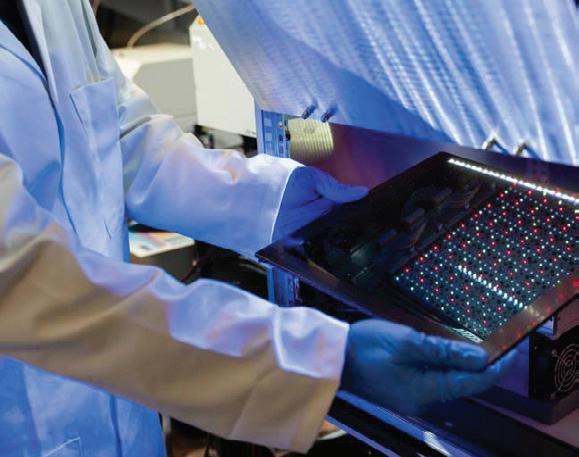
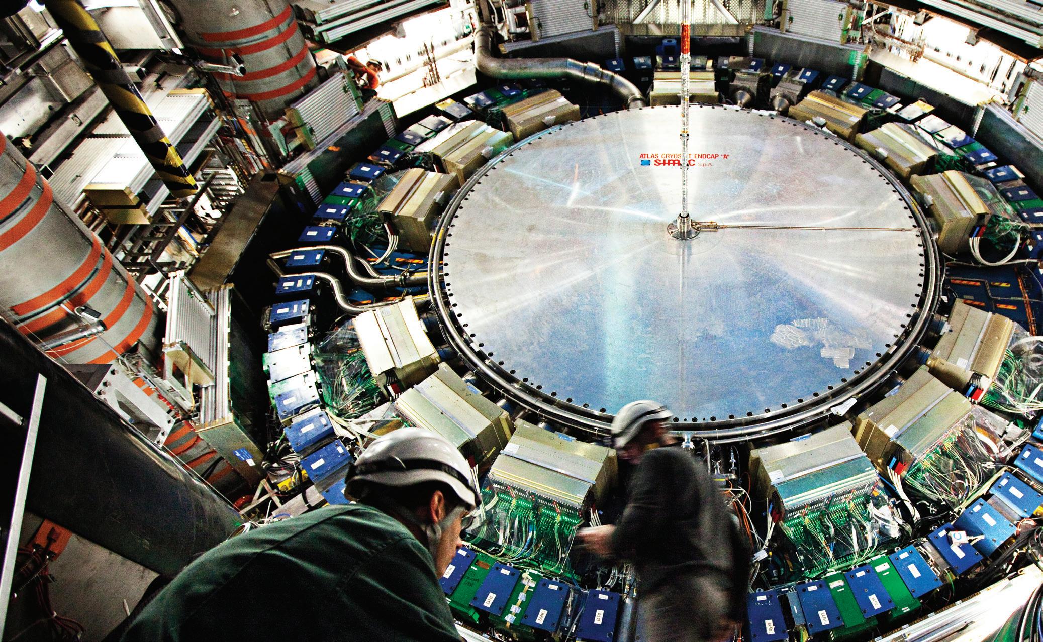
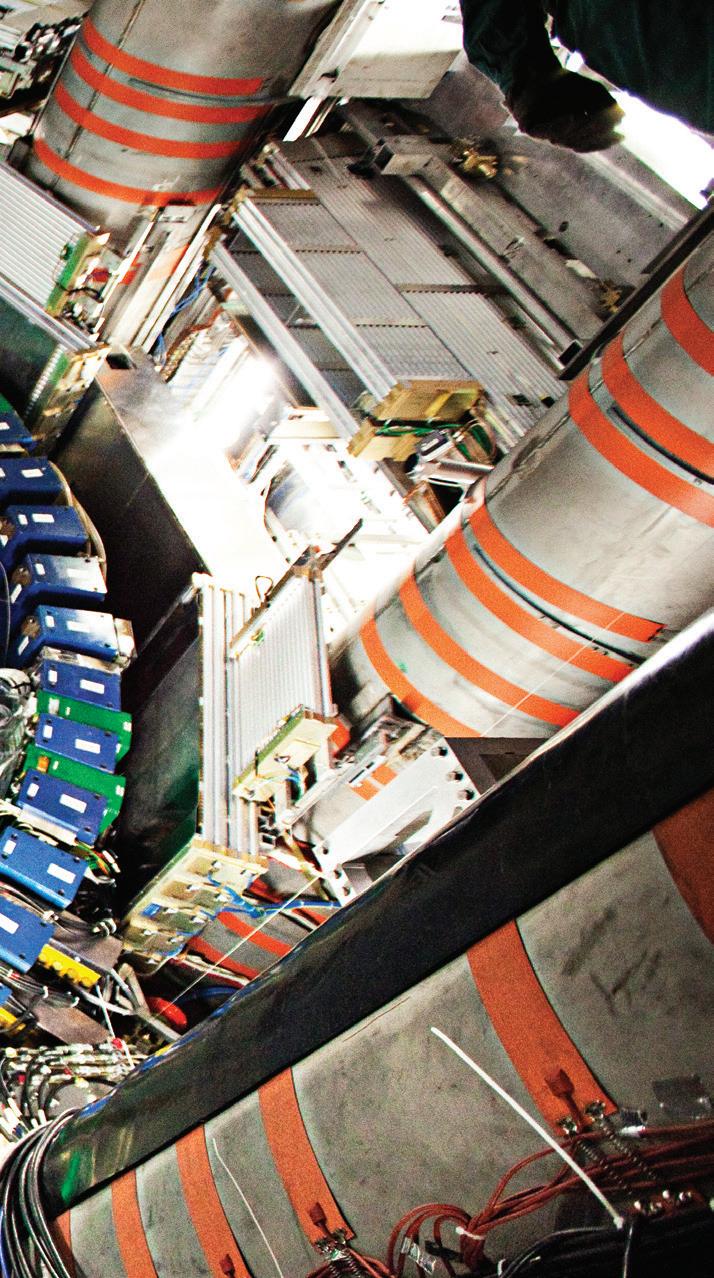
THE LARGE HADRON COLLIDER (LHC) IS TOUGH ON ELECTRONICS. SITUATED INSIDE A TUNNEL THAT RUNS IN A CIRCLE UNDER THE BORDER BETWEEN SWITZERLAND AND FRANCE, THE LHC ACCELERATES PARTICLES CLOSE TO THE SPEED OF LIGHT BEFORE SMASHING THEM TOGETHER. THE COLLISIONS YIELD TINY MAELSTROMS OF PARTICLES AND ENERGY THAT HINT AT ANSWERS TO QUESTIONS ABOUT THE BUILDING BLOCKS OF MATTER.
Those collisions produce an enormous amount of data — and enough radiation to scramble the bits and logic inside almost any piece of electronic equipment.
That presents a challenge to CERN’s physicists as they attempt to probe deeper into the mysteries of the Higgs boson and other fundamental particles. Off-the-shelf components simply can’t survive the harsh conditions inside the accelerator, and the market for radiation-resistant circuits is too small to entice investment from commercial chip manufacturers.
“Industry just couldn’t justify the effort, so academia had to step in,” said Peter Kinget, the Bernard J. Lechner Professor of Electrical Engineering at Columbia Engineering. “The next progress made by ATLAS will be triggered by one Columbia chip and measured by another.”
Kinget leads the team that designed specialised silicon chips that collect data in one of the harshest and most important environments in particle physics. Their most recent paper describing this project was published on 1 July in the IEEE Open Journal of the Solid-State Circuits Society.
“These sort of collaborations between physicists and engineers are very important to advancing our ability to explore fundamental questions about the universe,” said John Parsons, professor of physics at Columbia University and leader of the Columbia team working on the ATLAS detector, one of the LHC’s massive instruments. “Developing state-of-the-art instrumentation is crucial to our success.”
The devices the team designed are called analog-to-digital converters, or ADCs. Their task is capturing electrical signals produced by particle collisions inside CERN’s detectors and translating them into digital data that researchers can analyse.
In the ATLAS detector, the electrical pulses generated by particle collisions are measured using a device called a liquid argon calorimeter. This enormous vat of ultra-cold argon captures an electronic trace of every particle that passes through. Columbia’s ADC chips convert these delicate analog signals into precise digital

measurements, capturing details that no existing component could reliably record.
“We tested standard, commercial components, and they just died. The radiation was too intense,” said Rui (Ray) Xu, a Columbia Engineering PhD student who has worked on the project since he was an undergraduate at the University of Texas. “We realised that if we wanted something that worked, we’d have to design it ourselves.”
Designing “high-accuracy” reliability
Instead of creating entirely new manufacturing methods, the team used commercial semiconductor processes validated by CERN for radiation resistance
and applied innovative circuit-level techniques. They carefully chose and sized components and arranged circuit architectures and layouts to minimise radiation damage, and built digital systems that automatically detect and correct errors in real time. Their resulting design is resilient enough to withstand the unusually severe conditions at LHC for more than a decade.
Two Columbia-designed ADC chips are expected to be integrated into the ATLAS experiment’s upgraded electronics. The first, called the trigger ADC, is already operating at CERN. This chip, initially described in 2017 and validated in 2022, enables the trigger system to filter about a billion collisions each second and to instantly select only the most scientifically promising events to record. It serves as a digital gatekeeper deciding what merits deeper investigation.
The second chip, the data acquisition ADC, recently passed its final tests and is now in full production. The chip, which was
described in an IEEE paper earlier this year, will be installed as part of the next LHC upgrade. It will very precisely digitise the selected signals, enabling physicists to explore phenomena like the Higgs boson, whose discovery at CERN made headlines in 2012 and led to the Nobel Prize in physics in 2013, but whose exact properties still hold mysteries.
Both chips represent the kind of direct collaboration between fundamental physicists and engineers.
“The opportunity as an engineer to contribute so directly to fundamental science, is what makes this project special,” Xu said.
It further created opportunities to collaborate across multiple institutions. The chips were designed by electrical engineers at Columbia and at the University of Texas, Austin, in close collaboration with physicists at Columbia’s Nevis Laboratories and the University of Texas, Austin.

Power over Ethernet (PoE) simplifies deployment by removing the need for separate powerlines — cutting costs and speeding up installation. It also boosts energy efficiency, improves safety with low-voltage operation and reduces compliance costs. The PoE market is projected to grow at a 10.3% CAGR, with strong demand from power sourcing equipment (PSE) devices.
Fuelled by the rise of IoT and AI, PoE is being widely adopted in smart buildings, IoT gateways and power-overdata line (PoDL) applications for automation and in-vehicle systems. PSE technology, in particular, is increasingly used in autonomous mobile robots (AMRs) and humanoid robots — simplifying sensor deployment to accelerate rollout across retail, factory automation, logistics and agriculture.
As AMRs advance with diverse cameras and sensors to navigate dynamic environments involving moving workers, goods and other robots, PoE/PSE functionality becomes beneficial for streamlining device assembly and accelerating integration. However, developers often rely on off-the-shelf PoE injectors or ethernet modules with PSE capabilities. These solutions typically have a large footprint and require additional LAN ports — complicating implementation and disrupting design consistency in space-constrained AMR systems. Space limitations are only part of the challenge. Powered devices (PDs) in the environment — such as AI-enabled cameras and sensor gateways — also require simplified and rapid infrastructure integration through PoE technology. These devices are essential for collecting and relaying real-time data, enabling AMRs and other equipment to respond promptly and maintain smooth operations.
To improve operational efficiency without compromising safety, an AMR solution provider partnered with Advantech to develop a distributed computing system that offers full-field visibility — delivering an ‘eagle-eye’ view of the warehouse through a grid-like monitoring approach.
Simplified design and deployment of AMRs
Each AMR is equipped with 2D/3D cameras for SLAM, path planning and obstacle detection. These sensors primarily use ethernet for its flexibility, software control and precise time synchronisation via IEEE 1588. By integrating the MIOeM2LAN and MIOe-PSE extension modules with the AFE-R360 single board computer — powered by the Intel Core Ultra platform — the AMR system provides two additional PoE/PSE LAN outputs, streamlining the integration of PoE/ PD devices such as LiDARs and 3D stereo cameras, and accelerating AMR deployment without increasing system size.
Enable safe operation with optimised efficiency
To enable seamless collaboration with AMRs, the client deployed a ceiling-mounted smart camera system based on Advantech’s MIO-2364 Pico-ITX board, featuring an Intel processor and a customised PoE/PD module. With a compact footprint and PoE transmission, the system supports flexible, large-scale ceiling deployments and serves as an ‘eagle eye’ in the environment. It continuously monitors surroundings, processes data from AMRs and plans optimal routes. Its low-voltage operation minimises electrical risks and reduces compliance costs related to safety standards. This ceiling-to-ground collaboration also minimises AMR slowdowns, improves safety and reduces the need for redundant onboard camera and AI hardware.
Results
Adopting this new system substantially reduces instances where AMRs need to avoid collisions, stop or slow down, ultimately boosting operational efficiency in the facility by up to 30%.
Advantech Australia Pty Ltd www.advantech.net.au