RESEARCH TITLE
Ion Beam Based Advanced Material Characterization and Modification
Interplay between PTP1B activity and cholesterol metabolism
Role of the Phosphoprotein Phosphatase PTP1B in Cardiac Hypertrophy
Structure Function Studies - Regulation of PTPs by Redox Signaling
Bio Roll-Up
Fluorescent Plasmonic Sensors for Disease Diagnosis
Nanoelectronic Hardware for Neuromorphic Computing
-----and in-Memory Computing
EUV Photoresist Fundamentals
Applications of Machine Learning to Materials Characterization
Mueller Matrix Scatterometry Measurement of
-----3D DRAM structures fabricated with Si/SiGe multilayers
Corrosion Products: Hydrothermal Synthesis, Nanoparticle Characterization, and Transport Modeling
Back-End-of-the-Line Metals: Copper and “Beyond Copper”
Additive Nanomanufacturing using Charged Particle Beams
Nanoparticles for Chemical Mechanical Planarization
Li-Enriched Graphite Anodes of Batteries Investigated
-----using Nuclear Reaction Analysis
Engineering active sites on transition metals as high-performance bifunctional electrodes for electrochemical water splitting
Development of Nanostructured Antireflection Coatings
-----Technology for UV and IR Bands for Improved Detector
Array and Sensor Performance
Graphene Enhanced Charged Coupled Heterostructures for Mid-wave
-----IR Photodetectors & Focal Plane Arrays
Predictive Modeling for Energy Storage Cell Performance Optimization
Profiling the Budding Yeast Genome For Resistance to Food Carcinogens
On-demand Scalable Fabrication of Nanostructures
Scalable Telecom Single-Photon Emitters for Quantum Networks
Polarization-dependent Nanophotonic Devices
Ion Beam Research on Extreme-Condition
-----Materials and Harsh-Environment Sensing
Nanoscale Visualization of Electrostatic Barriers Formed at Material Interfaces
Hassaram Bakhru
Benoit Boivin
Benoit Boivin
Benoit Boivin
Robert L. Brainard
Nathaniel Cady
Nathaniel Cady
Greg Denbeaux
Alain Diebold
Alain Diebold
Kathleen A Dunn
Kathleen A. Dunn
Kathleen A. Dunn
Kathleen A. Dunn
Harry Efstahiadis
Harry Efstathiadis
Harry Efstathiadis
Harry Efstathiadis
Eric Eisenbraun
Michael Fasullo
Spyros Gallis
Spyros Gallis
Spyros Gallis
Mengbing Huang
Low Frequency Pulsed Power Electromigration
Epitranscriptomic Control of Senescence
Group III - Sb Alloys for Multilevel Phase Change Memory
Artificial Intelligence-Driven Adaptive Sensors for Autonomous Object Recognition
InAs/GaAs Quantum Dot Integrated Scintillation Detectors
Quantum Control of Electron States in Ballistic Waveguides
Neural Nets and AI in Biomedical Neuroscience
Transplantable Neuronal Circuitry for Spinal Cord Injury
Economics of Technological Change
A Search for Novel Efficient p-type Nitride Materials
Microwave activation-annealing of Mg-implanted GaN
GaN/AlGaN superlattices for infrared detection
Photocathodes for Detectors and High Brightness Electron Sources
Future Manufacturing: Development of Bio-hybrid Electronic and Photonic Devices
Novel Low-shear Bioreactor for Hematopoietic and Stem Cell Expansion
Production of a Bioengineered Heparin in Murine Mastocytoma Cells
Improving SiC Wafers and Processing for Lower Costs and Higher Reliability
Manufacturing of Ultra-high-voltage SiC devices (MUSiC)
Scalable, Manufacturable, And Robust Technology for SiC power integrated Circuits (SMART SiC Power ICs)
Development of Trench 1.2kV 4H-SiC MOSFETs
CPR (Cost competitive, high Performance, and Rugged) SiC Power Devices
For Electric Drive Technologies
Structurally Interacting RNA (sxRNA)
Density Functional Theory Analysis of Copper Grain Boundary Impurities
Area Selective Deposition - ASD
Plasma Etching
Surface Analysis of Ru Thin Films Used for MEMS Contacts
Micro-/Nanofiber Scaffolds for Salivary Gland Regeneration
Functional and Integrative Tissue Generation Center (FITGC)
Digital Transformation of Science, Economy, and Society
FACULTY NAME
Jim Lloyd
J. Andres Melendez
Serge Oktyabrsky
Serge Oktyabrsky
Serge Oktyabrsky
Serge Oktyabrsky
Janet L. Paluh
Janet L. Paluh
Unni Pillai
Shadi Shahedipour-Sandvik
Shadi Shahedipour-Sandvik
Shadi Shahedipour-Sandvik
Shadi Shahedipour-Sandvik
Susan Sharfstein
Susan Sharfstein
Susam Sharfstein
Woongje Sung
Woongje Sung
Woongje Sung
Woongje Sung
Woongje Sung
Scott Tenenbaum
Brad Thiel
Christophe Vallee
Christophe Vallee
Carl A. Ventrice
Yubing Xie
Yubing Xie
Yongqiang (Alex) Xue
Project Summary
Rutherford Backscattering- Channeling (RBS)
Nuclear Reaction Analysis (NRA)
High Resolution Magnetic Spectrometer
Particle induced X-ray analysis (PIXE)
Ion implantation
Micro-beam RBS/ PIXE Analysis


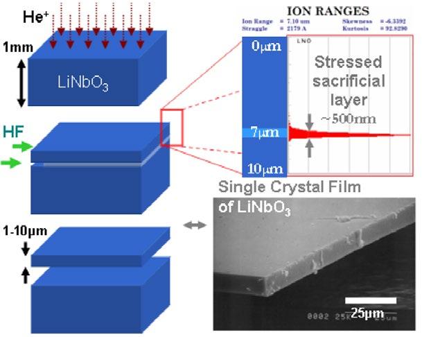
Crystal Ion slicing
FEOL : Dopant Activation, Diffusion
Studies in Si, SiGe, SOI. High resolution Depth profiling for USJ
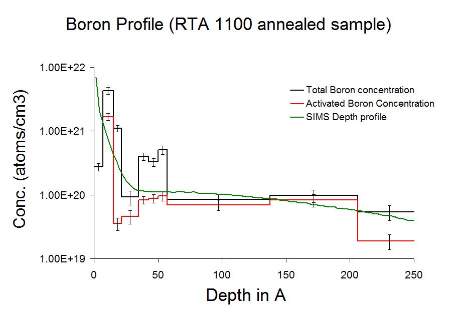
Defects in Semiconductor crystals: Ultra shallow junctions, Waveguides.


Publications
Manana, U., Shah, K., Chaudhary, L. S., Higashiya, S., Bakhru, H. S., Gittleson, F. S., & Efstathiadis, H. Analysis of SEI Formation and Fast Charging on Lithium Loss in NMC/Graphite Cells. In ECS Meeting Abstracts (No. 4, p. 512, 2021).
S. Higashiya, U. Manana, K. Shah, L. Chaudhary, M. Chebuske, A. Hagazy, H. Bakhru, F. Gittleson and H. Efstathiadis, “Analysis of SEI Formation and Fast Charging on Lithium Loss in NMC/Graphite Cells”, Fast Charging in Electrochemical Systems - Batteries and Supercapacitors, 240 Electrochemical Society Meeting, Virtual Conference, (2021).
M. Millares, H. Frost, M. Chebuske, K. Shah, D. Sadana, H. Bakhru and H. Efstathiadis, “Structural Analysis of Li1xAlxTi2-x(PO4)3Thin Films for All-Solid-State Li-ion Battery Applications, Physics of Corona viruses, 122nd Topical Symposium of the New York State Section of the American Physical Society, Virtual Conference, Albany, NY (2020).
S. Higashiya, A. Hegazy, K. Shah, L. Chaudhary, M. Chebuske, H. Bakhru, F. Gittleson and H. Efstathiadis, “Analysis of SEI Formation and Fast Charging on Lithium Loss in NMC/Graphite Cells”, submitted to Chem. Acta (2022).
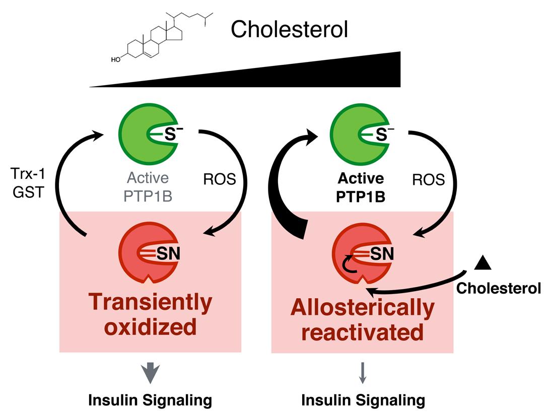
Much remains unknown about the underlying molecular mechanisms that cause insulin resistance. However, a growing body of data supports that altered physiological levels of cellular cholesterol is an underlying condition of insulin resistance. We have recently identified protein tyrosine phosphatase 1B (PTP1B) as a cholesterol-interacting protein in cells. Given that PTP1B dephosphorylates the insulin receptor on key residues and dephosphorylates insulin receptor substrate, we propose to investigate the link between cholesterol binding to PTP1B and insulin signaling. Our preliminary results show that cholesterol binds to PTP1B in vitro and in vivo. When characterizing this interaction, we have observed that cholesterol acts as an allosteric electron donor for PTP1B and that this electron tunneling event leads to the reduction of the reversibly oxidized catalytic cysteine of PTP1B, re-activates the enzyme and attenuates insulin signaling. Given these results, our proposal is designed to test the hypothesis that cholesterol is a reductant that protects PTP1B from NOX-mediated oxidation, and that PTP1B is a central player in the molecular mechanism by which increased cellular cholesterol leads to defective insulin receptor signaling and insulin resistance.
Publications
• He, P., Faris, S., Sagabala, R.S., Xu, Z., Callahan, B., Wang, C., Boivin, B., Zhang, F. and Linhardt R.J. (2022) Surface plasmon resonance cholesterol biochip for the study of cholesterol-protein interactions. Biosensors. 12(10):788
• Sagabala, R. S., Londhe, A. D., Marquart, K., Pappin, D., & Boivin, B. (2022). Role of PTP1B in the Regulation of Cholesterol Homeostasis. FASEB J., 36.
• Sagabala, S.R., Boivin, B. Role of Cholesterol and Oxysterols in Regulating PTP1B Activity. Free Radic Biol Med. 2017. 10: 223.
Acknowledgements
• Funding: NHLBI, American Heart Association.
• Collaborators: Robert Linhardt (RPI), David Jourd’heuil (AMC), Derek Pratt (U. Ottawa), Daniel Keedy (CUNY Manhattan), Wolfgang Peti (U. Connecticut),
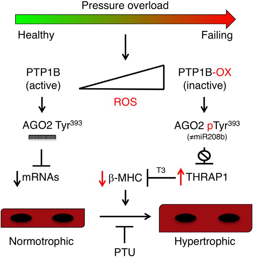
Oxidative stress is associated with reduced left ventricular function and correlates with the severity of heart failure in patients. Research from many labs now highlights the importance of reactive oxygen species as mediators of cardiomyocyte hypertrophy and the development of contractile dysfunction Despite intensive efforts, proteins targeted by ROS in hypertrophy remain mostly unknown to date We have recently demonstrated that Protein Tyrosine Phosphatase 1B (PTP1B) becomes reversibly oxidized and inactivated in pressure overload-induced cardiac hypertrophy and that PTP1B inactivation causes profound changes in thyroid hormone responsiveness. We showed that inhibiting the synthesis of triiodothyronine rescued the exacerbated pressure overload-induced hypertrophy and improved myocardial contractility and systolic function in cardiomyocyte-specific PTP1B knockout mice (PTP1B cKO) subjected to pressure overload We hypothesize that as hypertrophy develops, the inhibition of the cardioprotective activity of PTP1B by cellular oxidants leads to T3-mediated changes contributing to pathological hypertrophy Based on our recently published data in which we demonstrate that breaking the interaction between 143-3z and PTP1B prevents its inactivation in vivo, we also hypothesize that ectopic expression of a peptide derived from PTP1B, will both prevent the oxidation and inactivation of PTP1B in myocytes, and prevent pathological thyroid hormone signaling, left ventricular hypertrophy and heart failure
Publications
• Coulis, G. et al. (2022) Protein Tyrosine Phosphatase 1B Regulates miRNA-208b-Argonaute 2 Association and Thyroid Hormone Responsiveness in Cardiac Hypertrophy. Science Signaling 15(730): eabn6875.
• Londhe, A.D., et al. (2020) In Vitro Activity Assays to Quantitatively Assess the Endogenous Reversible Oxidation State of Protein Tyrosine Phosphatases in Cells. Curr. Protoc. Chem. Biol. 12, e84.
• Londhe, A.D., et al. (2020) Regulation of PTP1B Activation Through Disruption of Redox-Complex Formation. Nat. Chem. Biol. 16(2):122-125
Acknowledgements
• Funding: NHLBI, American Heart Association
• Collaborators: Gérard Karsenty (Columbia U.), Michel Tremblay (McGill U.), Jean-Claude Tardif (Montreal Heart Institute), Bruce Allen (Universite de Montreal)
Benoit Boivin
Studies - Regulation of PTPs by Redox Signaling
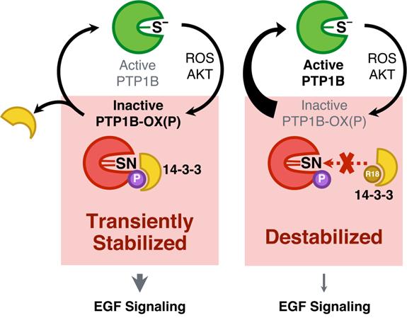
Previous studies on the structure of PTP1B have given us important insights on the catalytic function and redox regulation of members of the PTP family They have also revealed that the reversible oxidation of PTP1B (PTP1B-OX) leads to profound structural changes at the active site that can be taken advantage of by molecular tools such as conformation sensor antibodies to stabilize its inactive form. Although work from several labs, including ours, has clearly established that PTPs, and phosphatases from other families, are transiently oxidized by hydrogen peroxide in response to several cellular stimuli, our knowledge of the underlying mechanisms is rudimentary and inconsistent with most of the work in signal transduction from the last two decades that clearly points toward an exceptionally high level of specificity within signal transduction cascades This research project aims to gain further insight into the molecular mechanisms that regulate the catalytic activity of PTPs to develop molecules that specifically activate phosphatases
Publications
• Londhe, A.D., Bergeron, A., Rizvi, S. H., Kim, S.J., & Boivin, B. (2022). Characterization of Protein Tyrosine Phosphatase 1B activator peptides in cells. FASEB J, 36.
• Londhe, A.D., Bergeron, A., Zhang, F., Rizvi, SMH, Kim, S.J., Linhardt, R., Boivin, B. (2022) Characterization of Peptide Activators of Protein Tyrosine Phosphatase 1B, Free Radic Biol Med. 180, 63
• Londhe, A.D., et al. (2020) In Vitro Activity Assays to Quantitatively Assess the Endogenous Reversible Oxidation State of Protein Tyrosine Phosphatases in Cells. Curr Protoc. Chem. Biol. 12, e84
• Londhe, A.D., et al. (2020) Regulation of PTP1B Activation Through Disruption of Redox-Complex Formation. Nat. Chem. Biol. 16(2):122-125
Acknowledgements
• Funding: NHLBI, American Heart Association, SUNY Seed funding
• Collaborators: Robert Linhardt (RPI), Daryl Pappin (Cold Spring Harbor Laboratory), Nicholas Tonk (Cold Spring Harbor Laboratory), Elias Arner (Karolinska Institute), Seung Jun Kim (Korea Research Institute of Bioscience & Biotechnology)
Benoit Boivin
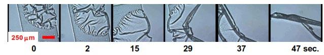
• The overarching goal of this proposal is to develop a self-assembly process to convert planar sheets of epithelial cell monolayers into 3D functional structures. To achieve this goal we will create trilayer stacks of photoimageable, biocompatible hydrogels for cell growth and use differential swelling stresses to self-assemble them into tubes, intersections and spheres for cell differentiation and functional tissue formation.
• We have created a biocompatible polymeric system that self-assembles.
• The current plan is to use thermallyresponsive polymers to control the timing of self-assembly so that we can vary selfassembly vs. the life-time of cell growth.
• Figure 1 shows (A) Idealized selfassembled tube lined with cells. (B) Idealized self-assembly structure.
• Figure 2 shows the first self-assembly results.
• Other than undergraduate posters, this work has intentionally been unpublished. The plan is to achieve critical results then, submit to a high-level journal.
• This work is has received a small amount of funding from the office of research. Mostly, however, this project has been self-funded and 98% of the research has been conducted by undergraduates.
Robert L. Brainard
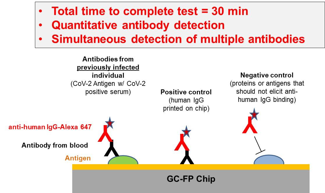
We are developing novel approaches to disease diagnosis and evaluation of serological response to infections or vaccination, in response to the COVID-19 pandemic and other important diseases.
Using Ciencia, Inc ’s grating-coupled fluorescent plasmonic (GC-FP) platform, we have developed assays for diagnosing Lyme disease with higher accuracy than conventional testing approaches, and for determining prior infection status/ vaccination status for COVID-19. This technology utilizes nanoscale plasmonic gratings fabricated at SUNY Poly.
In collaboration with the University of Rochester and other partners in the AIM Photonics program, we are working to develop rapid, label-free detection of COVID-19 serological (antibody) response using novel silicon-photonic devices fabricated in the SUNY Poly 300mm cleanroom
Publications
B. Taubner et al. Dual detection of COVID-19 antigens and antibodies using nanoscale fluorescent plasmonic substrates. (2022) Experimental Biology and Medicine. https://doi.org/10.1177/15353702221113860
B. Taubner et al. Rapid and Quantitative Detection of Human Antibodies Against the 2019 Novel Coronavirus SARS CoV2 and its Variants as a Result of Vaccination and Infection. (2021) Microbiology Spectrum. 9(2): e00890-21. https://doi.org/10.1128/Spectrum.00890-21
Acknowledgements
• SUNY Seed Funding
• AIM Photonics
• NIST “RACER” program
• NYS Biodefense Fund
Nathaniel Cady
Highlights
Grating-coupled fluorescent plasmonics (GC-FP) can be used to detect antibodies in human blood samples to diagnose disease or prior infection in less than 30 min.
N. Cady et al. Multiplexed Detection and Quantification of Human Antibody Response to COVID-19 Infection Using a Plasmon Enhanced Biosensor Platform. (2021) Biosensors & Bioelectronics. 171:112679. https://doi.org/10.1016/j.bios.2020.112679
J.S. Cognetti et al. Disposable photonics for costeffective clinical bioassays: application to COVID-19 antibody testing. (2021) Lab on a Chip. 21: 2913-2921 https://doi.org/10.1039/D1LC00369K
• Ciencia, Inc. (Mansfield Ctr., CT)
• Klemen Strle (NYS Dept. of Health)
• Benjamin Miller (U. of Rochester)
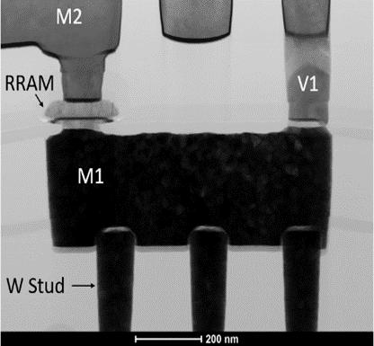
We have established an ongoing research program on resistive memory devices (aka: ReRAM). These metal-insulator-metal (MIM) devices behave similarly to neural synapses, as their “memory state” depends on the current and voltage history of the device This is a good example of bioinspired/biomimetic research, since the biological process of synapse formation is mimicked by a physical, electronic device. We have previously developed ReRAM as both non-volatile memory (NVM) elements, as well as devices to control the reconfigurability of CMOS circuits
To date we have developed a full 65nm CMOS/memristor hybrid chip design and fabricate these devices in the SUNY Poly 300mm fabrication facility. This work leverages a 65nm node CMOS process design kit (PDK) that has been licensed by the Research Foundation for SUNY for design and fabrication purposes – to which we have added a ReRAM module
We have ongoing efforts to characterize the switching mechanism of our devices, to better enable modeling and simulation of memristors in complex circuits We are also investigating methods (both fabrication methods and testing methods) that reduce the stochastic nature of memristor device performance This will improve reliability of these devices and make the amenable to larger scale integration with complex CMOS circuits, processors, etc
Publications
S. Rafiq, M. Abedin, K. Beckmann and N. C. Cady, Detecting Temporal Correlation on HfO2 Based RRAM on 65nm CMOS Technology. (2022) 2022 IEEE 31st Microelectronics Design & Test Symposium (MDTS) p. 1-6, https://doi.org/10.1109/MDTS54894.2022.9826965
M. Liehr, K. Beckmann, N. Cady. Impact of Switching Variability, Memory Window, and Temperature on Vector Matrix Operations Using 65nm CMOS Integrated Hafnium Dioxide-based ReRAM Devices. (2022) IEEE 31st Microelectronics Design & Test Symposium (MDTS), 2022. https://doi.org/10.1109/MDTS54894.2022.9826924
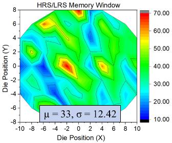
A TEM cross-section of an integrated transistor-ReRAM (1T1R) cell is shown at right, and full 300mm wafer map showing the memory window (high resistance vs. low resistance level) for ReRAM devices fabricated in our 300mm fabrication facility.
Rafiq, J. Hazra, M. Liehr, K. Beckmann, M. Abedin, J.S. Pannu, S.K. Jha, N.C. Cady. Investigation of ReRAM variability on flow-based edge detection computing using HfO2-based ReRAM arrays. (2021) IEEE Transactions on Circuits and Systems. https://doi.org/10.1109/TCSI.2021.3072210
M. Abedin, M. Liehr, K. Beckmann, J. Hazra, S. Rafiq, N. C. Cady. In-memory Computation of Error-Correcting Codes Using a Reconfigurable HfOx ReRAM 1T1R Array. (2021) 2021 IEEE International Midwest Symposium on Circuits and Systems (MWSCAS). p. 593-598, doi: https://doi.org/10.1109/MWSCAS47672.2021.9531717
J. Hazra, M. Liehr, K. Beckmann, M. Abedin, S. Rafiq, N.C. Cady. Optimization of Switching Metrics for CMOS Integrated HfO2 based Bipolar RRAM Devices on 300 mm Wafer Platform. (2021) IEEE International Memory Workshop (IMW) 2021 1-4. DOI: 10.1109/IMW51353.2021.9439618
• Air Force Research Laboratory, NSF, Xallent, LLC, IBM- SUNY AI Alliance
• The latest generation lithography technology for semiconductor manufacturing is extreme ultraviolet (EUV) lithography
• It has begun production for advanced semiconductor devices, but still there are challenges with the photoresist used for the light sensitive pattern formation.
• We study multiple aspects related to the fundamental reaction mechanism of EUV photoresists
• In the traditional chemically amplified photoresists, we study the generation of the acid from the photoacid generator and its efficiency to EUV photons
• We study the range of the acids generated which impacts the speed and resolution of the resist.
• We also study the diffusion rate and time scale of the acid diffusion
• At a small enough spatial scale nothing is uniform For photoresists, we have approached the regime where the actual molecular distribution in the photoresists becomes a statistical challenge for repeatable and reliable lithography
• The random molecular distribution can be calculated. We are studying the non-random molecular distribution that occurs during the coating and baking of the photoresist coated wafers. This leads to local resist non-uniformities like this resist pattern on the left side from a uniform exposure process.
• Changing the chemical composition to molecules that are known to have energetically favorability to segregate makes the system even worse as shown in the right image.
• Studying the onset of this segregation helps to understand how to control the segregation within commercial EUV photoresists where smaller numbers of segregated defects and smaller size features impacts manufacturability with EUV lithography
This research project is funded by the SRC, and multiple semiconductor companies
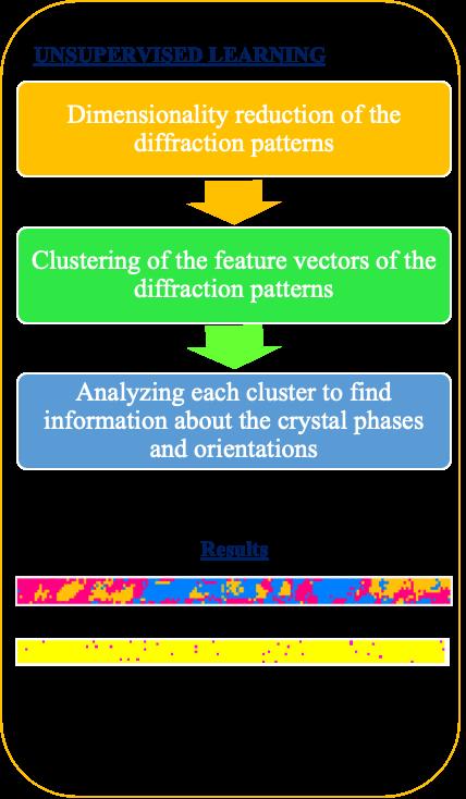
• The goal of this project is to access the ability of machine learning methods to improve the speed and accuracy of materials characterization.
• The first application is determination of crystal phase and orientation of ferroelectric HfZr oxide dielectric films used in advanced transistors.
• Data set consists of maps of electron diffraction patterns from cross-sectional samples of metal/HfZr oxide/metal samples.
• Sample provided by TEL
• Amir Kordijazi (Post-Doc)
Highlights
• First approach was un-supervised Machine Leaning.
Publications
• In-Line Metrology for Semiconductor Manufacturing: Tutorial – 2022 Frontiers of Characterization and Metrology for Nanoelectronics (FCMN 2022)
• Poster – Amir Kordijazi - Machine learning-assisted characterization of hafnia-based ferroelectric thin films FCMN 2022
• Co-Author : Implementation of High-Performance and High-Yield Nanoscale Hafnium Zirconium Oxide based Ferroelectric Tunnel Junction Devices on 300mm Wafer Platform, accepted (J. Vac. Sci. Technol. B, 2022)
• Conference Co-chair for 2022 Frontiers of Characterization and Metrology for Nanoelectronics.
Acknowledgements
•Funding: TEL Technology Center America - Gert Leusink
•Collaboration at TEL with Gert Leusink, Steve Consiglio, Sara Lombardo, etc.
•Collaboration at Georgia Tech with Asif Khan and Josh Kantor
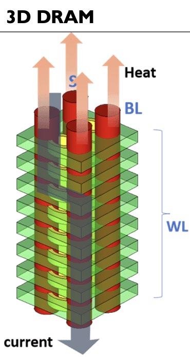
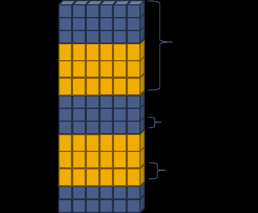
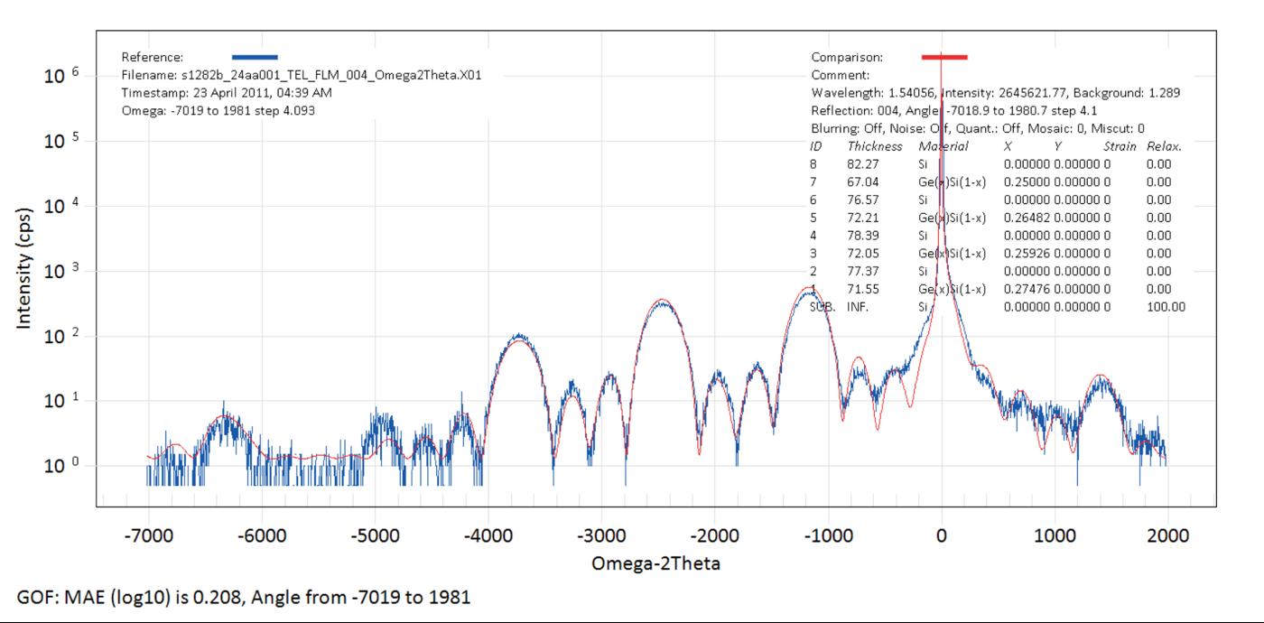
Mueller Matrix Scatterometry Measurement of 3D DRAM Structures
Fabricated with Si/SiGe Multilayers
• The goal of this project is to advance the ability of Mueller Matrix Spectroscopic Ellipsometry to measure 3D DRAM structures.
• Ezra Mel Pasikatan (Grad Student)
• Another goal is to characterize the multilayer single crystal epilayers of Si/Si1-xGex using XRay and other methods.
• Develop scatterometry models for measuring the shape and dimensions of test structures with lithographically patterned contact holes and cavity etches.
https://semiengineerin g.com/will-monolithic3d-dram-happen/
• Superlattice effect observed in X-Ray Data (ω 2���� ) data from initial samples
• Favorable comparison between ellipsometry and XRay analysis of un-patterned film stack.
• Invited Talk : Determination of Nanostructure Shape and Dimension using Mueller Matrix Spectroscopic Ellipsometry : International Conference on Spectroscopic Ellipsometry 9
• Co-Author: Optical and Electrical Properties of Nanoscale Materials (Springer, Dec. 2021)
• Conference Co-chair for 2025 International Conference on Spectroscopic Ellipsometry (Boulder Co).
• Funding: Onto Innovations, Andy Antonelli
• Collaboration at TEL with Subhadeep Kal for samples
adiebold@albany.edu
https://link.springer.com/book/10.1007/978-3-030-80323-0
Corrosion
Characterization, and Transport Modeling
Nickel ferrite particles form when metal alloys containing nickel and iron corrode in high temperature water, and can be transported downstream to deposit in less auspicious locations. Deposition in a particular location is a function of many variables including the flow characteristics, particle size distribution, as well as particle -particle and particle-surface interactions. However, studying these deposits in the field is prohibitive due to the harsh environment in which they are formed Instead, we synthesize model particles in a controlled laboratory setting, and evaluate surface charge and magnetic characteristics as a function of synthesis conditions and composition Information about particleparticle or particle -surface interactions is then incorporated into a COMSOL Multiphysics model of the flow system, to predict nanoparticle transport and deposition in real environments Controlling these material characteristics will also enable tailoring of ferrite nanoparticles for future applications in catalysis, magnetic storage systems, and the production of magnetic fluids
• Non-stoichiometric nanoparticles were synthesized over a range of metal cation ratios and temperatures
• Phase identification by X-ray Diffraction enabled the generation of a phase diagram with a goal of identifying the window for obtaining single phase nickel ferrite product
• Zeta potential measurements based on particle size & composition are used to calculate transport & deposition probability in COMSOL
• B.S. Nagothi, J. Arnason and K.A. Dunn, “A Hydrothermal Phase Diagram for the Low-Temperature Synthesis of Non-stoichiometric Nickel Ferrite Nanoparticles,” accepted for publication in Nuclear Technology, 2023
• B.S. Nagothi, J. Arnason and K.A. Dunn, “A Hydrothermal Phase Diagram for the Low-Temperature Synthesis of Non-stoichiometric Nickel Ferrite Nanoparticles,” poster presented at the 20th International Conference on Environmental Degradation of Materials in Nuclear Power Systems – Water Reactors, Snowmass, CO, July 17-21, 2022
• B.S. Nagothi, “Synthesis of nonstoichiometric nickel ferrites by hydrothermal method,” Master ’s Report, College of Nanoscale Science & Engineering, SUNY Polytechnic Institute, 2022.
• This material is based upon work supported by the U.S. Nuclear Regulatory Commission, Office of Nuclear Regulatory Research under Award Number 31310020M0006
Kathleen A. Dunn
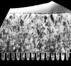
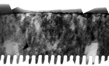
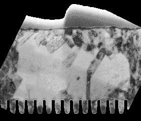
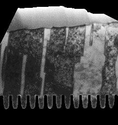
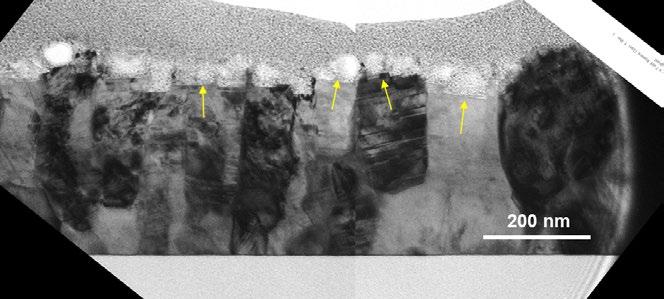
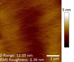
Electroplated copper has been the conductor of choice for the semiconductor industry for twentyfive years, but faces a rapidly approaching sunset of its utility as chips and their interior wiring continue to scale to smaller sizes. My group has worked on several aspects of this issue over the last twenty years, from deposition method development for copper and its alloys, to microstructural manipulation for resistance to electromigration failure, to plasma etching and chemical mechanical polishing of alternative metals. The overarching theme is the role of defects in determining and manipulating material performance, a connection we explore with cutting-edge microscopy and spectroscopy techniques applied to blanket and patterned wafers from the 300-mm fabrication line.
• Time-resolved Transmission Electron Microscopy confirmed microstructural transformation of ECD copper was initiated at sub-surface interface; later shown to depend on seed orientation
hours after plating 2.5 hours after plating
• Alloy development Cu(Co), Cu(Ag), Cu(Sn) for grain boundary stabilization
hours after plating
hours after plating
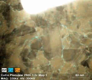


• Microstructural dependence of etch response in Ru


• S. Rogalskyj, “Ruthenium Fuzz Growth and Surface Faceting During O2/Cl2/Ar Plasma Processing,” M.S. report, College of Nanoscale Science & Engineering, SUNY Polytechnic Institute, 2022.
• S. Rogalskyj, H. Frost, L. Melican, A. Palka, N. Joy, D.Triyoso, R. Clark, C. Wajda, G. Leusink, A. Raley, and K. Dunn, “Plasma-induced roughness and chemical modification of TiN bottom electrode and their impact on HfO2-MIM properties,” Proceedings of the 2020 International Interconnect Technology Conference. Winner, Best Student Paper.
• C. Netzband and K.A. Dunn, “Ceria Based Chemical Mechanical Polishing Slurries,” US Non-Provisional Patent Application 17/069,608, filed October 14, 2020.
• C. Netzband and K.A. Dunn, “Improving BEOL Metal Polishing through the Use of Ceria Abrasives,” Proceedings of the 2019 International Conference on Planarization/CMP Technology. Winner, Best Student Presentation.
• T. Tsurumaru, L. Prestowitz, B. O’Brien and K. Dunn, “The impact of solute segregation on grain boundaries in dilute copper alloys,” Proceedings of the 2018 International Interconnect Technology Conference (IITC) , (2018). DOI: 10.1109/IITC.2018.8430454
Acknowledgements
• This work has been funded by the Semiconductor Research Foundation, SUMCO Corporation of Japan, and the National Science Foundation Division of Materials Research.
Kathleen A. Dunn
Focused Electron Beam Induced Deposition (EBID) and its corollary Ion Beam Induced Deposition (IBID) are direct-write techniques capable of producing three-dimensional structures with high spatial resolution, high placement fidelity, and the flexibility to deposit on non-planar surfaces While roomtemperature EBID and IBID with gas-phase precursors are commercially available options from any electron or ion microscope manufacturer, the growth rate is too slow to be viable for anything but laboratory use. Improving throughput without comprising the site-specificity or 3-dimensional capabilities of the technique are critical if this technology is to be a credible micro- or nano-manufacturing option. Using a unique custom-built cryogenic stage, my group was able to move the reaction from the typical precursor-starved regime into a precursor-rich regime where the growth rate was controlled by the electron beam current. We are the only group, globally, which employs this cryogenic assistance, which has enabled us to set (and keep) the current world record for volumetric growth rate for EBID depositions.
• Demonstrated three orders of magnitude faster volumetric growth rates than our nearest competitor.
• Demonstrated the ability to design and build suspended structures, including stacked, freestanding bridges.
• Demonstrated morphological control in three regimes: mesh, smooth and rough surfaces.
• Elastic and plastic responses are intermediate between polymer and metals.


• A. Reiser, L. Koch, K.A. Dunn, F. Iwata, O. Fogel, Z. Kotler, N. Zhou, K. Charipar, A. Pique, P. Rohner, D. Poulikakos, S. Lee, S. K. Seol, I. Utke, C. van Nisselroy, T. Zambelli, J. M. Wheeler and R. Spolenak, “Metals by micro additive manufacturing: a comparison of microstructure and mechanical properties,” Advanced Functional Materials, 2020, 1910491. DOI: 10.1002/adfm.201910491
• M. Bresin, M. Toth and K.A. Dunn, “Direct-write 3D Nanolithography at Cryogenic Temperatures,” Nanotechnology 24(3), 03501 (2013). DOI: 10.1088/0957-4484/24/3/035301
Acknowledgements
• This work has been funded in part by FEI Corporation (Thermo Fisher Scientific).
Kathleen A. Dunn
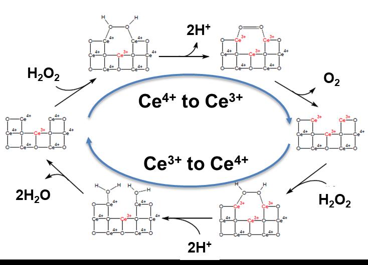
Chemical Mechanical Planarization (CMP) is the secondmost costly process in the production of semiconductor wafers, and much of that cost comes from consumables such as the aqueous slurries used for material removal and surface polishing Although the pH and solid content of slurries are adjusted during reuse to account for dilution of the liquid, very little is known about changes to the nanoparticles themselves. We design materials and methods to extend the usable lifetime of slurries, optimize their surface characteristics to increase their efficiency, and to inform occupational health strategies for ameliorating worker exposures.
• Developed new methods and metrics for evaluating particle agglomeration in traditional slurries, and used this metric to design an AI algorithm to predict slurry replacement timing
• Broke the trade-off between speed and performance in ceria slurries by using the catalase mimetic activity of cerium to enhance the concentration of Ce3+ on the particle surface, independent of particle size
• C. Netzband and K.A. Dunn, “Ceria Based Chemical Mechanical Polishing Slurries,” US Non-Provisional Patent Application 17/069,608, filed October 14, 2020.
• C. Netzband and K. Dunn, “Improving Ruthenium Polishing Through the Use of Ceria Abrasives,” Proceedings of the 2020 International Interconnect Technology Conference (virtual), 2020.
• C. M. Netzband and K. Dunn, “Controlling the Oxidation State During Silicon Oxide CMP to Improve Material Removal Rate and Roughness,” ECS J. Solid State Sci. Tech. 9, 044001, 2020. DOI: 10.1149/21628777/ab8393
• C. Netzband and K.A. Dunn, “Investigation into the Effect of CMP Slurry Chemicals on Ceria Abrasive Oxidation State using XPS”, ECS J. Solid State Sci. Tech. B, (10), P629-P633, 2020. DOI: 10.1149/2.0311910jss
• M. Kubota, K. Takanashi and K.A. Dunn, “Evaluation of Particle Agglomeration Level in CMP Slurry for Silicon Wafers and Investigation of these Effects on the Polishing Behaviors,” Proceedings of the 2019 International Conference on Planarization/CMP Technology
• C. Netzband and K.A. Dunn, “Improving BEOL Metal Polishing through the Use of Ceria Abrasives,” Proceedings of the 2019 International Conference on Planarization/CMP Technology. Winner, Best Student Presentation.
Acknowledgements
• This work has been funded in part by SUMCO Corporation of Japan.
Kathleen A. Dunn
Lithium-ion electrode-electrolyte interfaces remain key areas of study, even after a half-century of technological development. The physical and chemical characteristics of the solid electrolyte interphase (SEI) formed on a graphite anode surface during the initial charge cycle may have an outsized influence on cell performance. Ideally, the electrolyte selection, formation, and resulting SEI are designed to optimize cell parameters like lifetime, energy, and power while balancing the process time and its associated production cost
Non-destructive Li nuclear reaction analysis (NRA) techniques at Ion Beam Lab of the University at Albany were used to profile the Li distribution at the surface of graphitic Li-ion battery anodes. These techniques show that Li concentrations are elevated within 300 nm of the anode surface, even in fully delithiated states The surface region, which includes the solid electrolyte interphase, contains at least 60% of the total Li irreversibly lost during formation and cycling leading to battery degradation.
Publications
• Using two Li-NRA techniques PIGE and DIPE, we obtained quantifiable 6Li and 7Li depth profiles of graphite anodes after SEI formation and cycling
• These non-destructive techniques illuminate Li concentration gradients at electrode surfaces and elucidate the consequences of electrochemical irreversibility
• Nuclear reaction analyses will continue to be useful in studies on the physical and performance impacts of SEI formation, cell aging, and fast charging in Liion batteries.
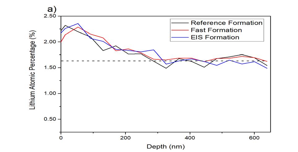
• PIGE 7Li depth profile of the formed and cycled graphite anode surface Each line indicates a representative anode from a cell subjected to a different formation procedure. A background that is consistent for each sample is indicated as a dashed line
• M. Chebuske, S. Higashiya, S. Flottman, H. Bakhru F. Gittleson, B. Antonopoulos, O. Paschos and H. Efstathiadis, “Lithium-Enriched Graphite Anode Surfaces Investigated using Nuclear Reaction Analysis”, Chem. Comm., 93 (2020), DOI: 10.1039/d0cc04205f
• S. Higashiya, U. Manana, K. Shah, L. Chaudhary, M. Chebuske, A. Hagazy, H. Bakhru, F. Gittleson and H. Efstathiadis, “Analysis of SEI Formation and Fast Charging on Lithium Loss in NMC/Graphite Cells”, Fast Charging in Electrochemical Systems - Batteries and Supercapacitors, 240 Electrochemical Society Meeting, (2021).
Acknowledgements
• This research was supported by the New York State Center for Advanced Technology in Nanomaterials and Nanoelectronics (CATN2) and by the BMW Group.
• Collaborators: J. Mckinney (BMW), F. Gittleson (BMW), M. Pentaris (Custom Electronics), W. Lamford (Univ. at Albany), H. Bakhru (SUNY Poly), I Gherasoiu (SUNY Poly).
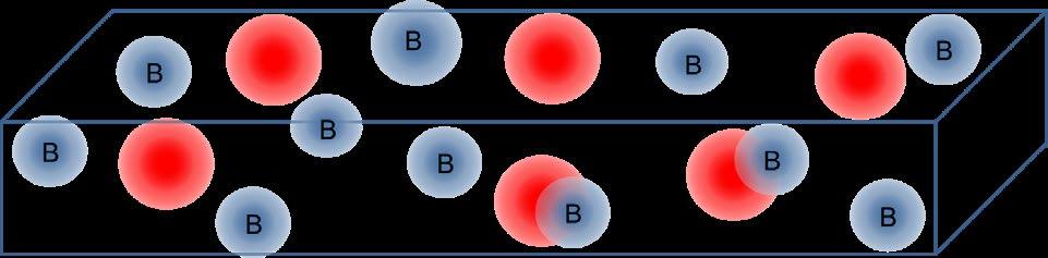
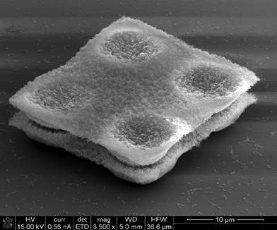
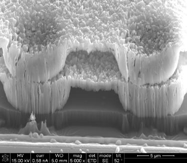
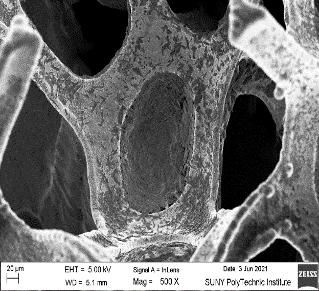
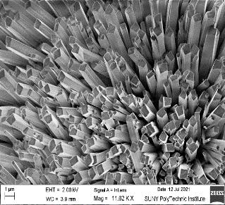
Engineering Active Sites on Transition Metals as HighPerformance Bifunctional Electrodes for Water Splitting Electrochemical
A facile method was used to prepare MoNi4 particles on MoO2 nanorods and MoVN was coated using DC-RF cosputtering technique. Coating transition metal nitride (MoVN) on synthesized nanorods showed significant increase in the catalytic activity towards both HER and OER with measured overpotentials of 14 mV and 140 mV at 10 mA/cm2 respectively
Electrochemical impedance spectroscopic results also show the decreased charge transfer resistance of the synthesized electrode for both half-cell reaction.
The stability tests of the electrode were also performed for both reactions under consideration, showing that the electrode can deliver the expected current density for 12 hours without degradation.
Further, the required overpotential for overall water splitting was found as low as 320 mV and the continued electrolysis performed for 12 hours at high current density, demonstrates the applicability of the electrode synthesized in commercial H2 production technologies Harry Efstathiadis
• MoNi4-MoO2/Ni foam was synthesized via facile hydrothermal method.
• MoVN was coated using DC-RF co-sputtering on NiMoO4 nanorods.
• Fabricated electrodes performed very well for both cathodic and anodic reactions in alkaline conditions with overpotentials only 14 mV and 140 mV respectively
• The electrodes also proved to be stable for both HER and OER for 12 hours without reduction in current density.
• Testing in flow electrode conducted reduced the bubble resistance and also increased overall efficiency
Publications
Y. Kumaran et al 2022 Meet. Abstr MA 2022-02 2523
Y. Kumaran, I. Gherasoiu, M. Thandavarayan, . Efstathiadis, “Engineering active sites on transition metals as highperformance bifunctional electrodes for electrochemical water splitting” submitted to ACS Catalysis (2023).
Acknowledgements
• New York State Center of Excellence in Nanoelectronics and Nanotechnology (CENN).
• Collaborators: Y. Kim (Univ. at Albany), I Gherasoiu (SUNY Polytechnic). A. Teli (S. Korea), M. Thandavarayan (India), Y. Kim (Univ. at Albany).
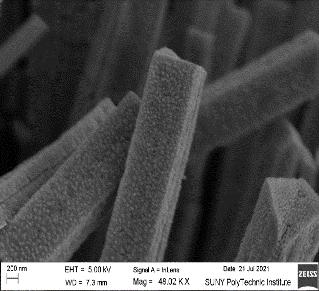

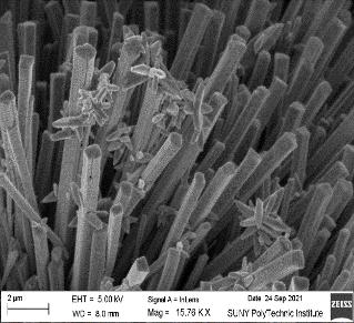
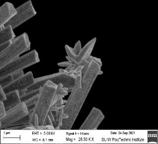
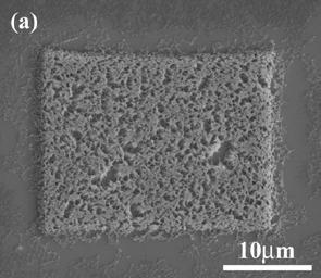
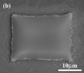
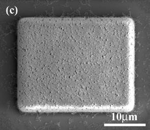
Figure above: SEM imaging (a) Ni foam (b) NiMoO4 H2O obtained through hydrothermal synthesis (c) MoNi4/MoO2/Ni foam after annealing for 180 minutes (d)&(f) MoVN nanoflakes on MoNi4/MoO2 nanorods
Technology for UV and IR Bands for Improved Detector Array and Sensor Performance
Nanostructured antireflection (AR) coatings reducing optical reflections and maximizing radiation transmitted onto the surfaces of substrates, optics and optical devices such as detectors over ultraviolet (UV) to infrared (IR) wavebands have many potential optical applications including for NASA IR band detectors.
These AR coatings fabricated using a scalable e-beam deposition process on GaSb substrates and LWIR detector arrays provide omnidirectional suppression of light reflection and increased optical transmission over a range of incident IR angles for improved detection and sensing performance. Through nanoengineering optical layers and tuning their refractive indexes, broadband and omnidirectional suppression of light reflection and scattering is achievable with increased optical transmission for enhanced IR detector and system performance over a wide range of light incidence angles.
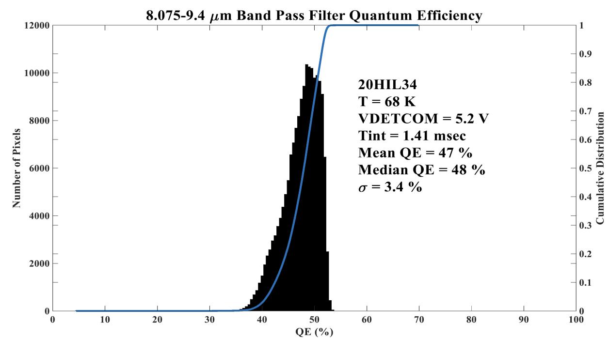
The growth of step-graded nanostructured layers using a process involving deposition at different tilt angles has produced single-layer AR coatings utilizing ZnS demonstrating below 4% reflectance, compared to ~34% reflectance for uncoated GaSb, across LWIR bands of interest with substantial improvement in quantum efficiency.
Publications
• AR nanostructures were developed to create optimal AR coatings with high laser damage thresholds and high reliability, even in extreme low temperature environments and under launch conditions.
• The quantum efficiency (QE) of a focal plane array after being coated with these nanostructured AR coatings improved from 31% to 47% from 8.0-9.4 μm over the LWIR band.
• These tunable nanoengineered optical layers enable the realization of optimal nanostructured coatings with extended reliability in extreme low temperature environments and under launch conditions.
• A. K. Sood, J. W. Zeller, A. W. Sood, P. Ghuman, S. Babu, S. Gunapala, A. Soibel, D. Ting, L. S. Chaudhary, and H. Efstathiadis, “Nanostructured antireflection coating technology for enhanced MWIR and LWIR band sensing performance,” Proc. SPIE. 12234, 1223424 (2022).
• A. K. Sood, J. W. Zeller, A. W. Sood, R. E. Welser, P. Ghuman, S. Babu, S. Gunapala, A. Soibel, D. Ting, L. S. Chaudhary, and H. Efstathiadis, “Improved UV to IR band detector performance through advanced nanostructured antireflection coatings,” Proc. SPIE 12091, 1209106 (2022).
• A. K. Sood, J. W. Zeller, A. W. Sood, R. E. Welser, P. Ghuman, S. Babu, S. Gunapala, A. Soibel, D. Ting, L. S. Chaudhary, and H. Efstathiadis, “Development of nanostructured antireflection coating technology for IR band for improved detector performance,” in Proc. SPIE 11858, 1185812 (2021).
This research has been funded by the National Aeronautics and Space Administration (NASA), Contract No. 80NSSC20C0151.
Harry Efstathiadis
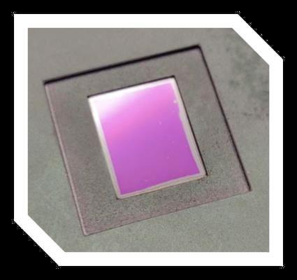
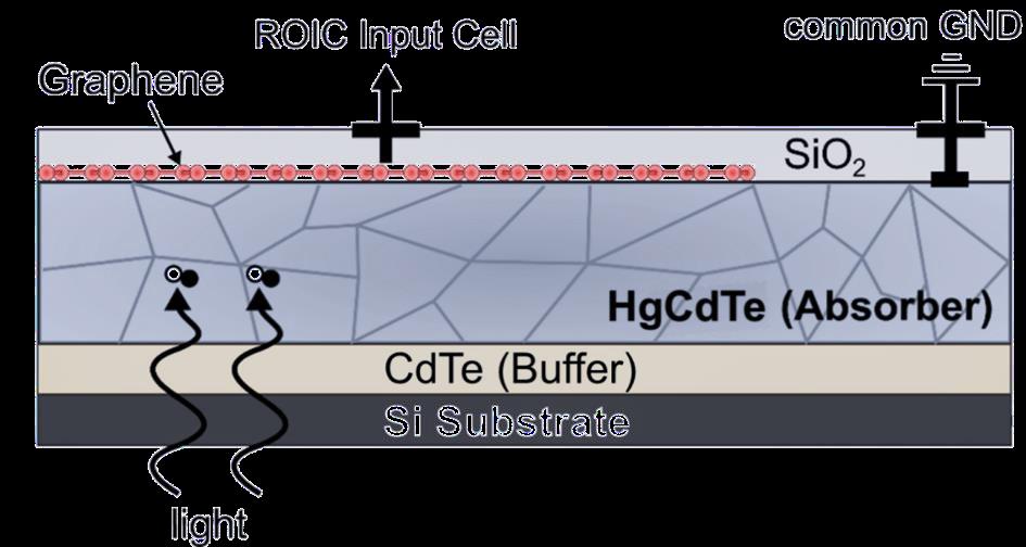
High performance detector technology was developed for sensing over the mid-wave infrared (MWIR) band that involves the integration of graphene with HgCdTe photodetectors.
It combines the best of both materials, making them much more practical and useful for MWIR sensing applications such as remote sensing and earth observation, e.g., in smaller satellite platforms (CubeSat), for measurement of thermal dynamics with better spatial resolution. The graphene functions as high mobility channel that whisks away carriers before they can recombine, further contributing to performance. Chemical doping of the bilayer graphene lattice has provided p-type doping levels in graphene for high mobility implementation in high performance MWIR HgCdTe detectors Through modeling, material development, and device optimization, room temperature graphene-HgCdTe MWIR array detectors were demonstrated.
Publications
Highlights
• High-performance graphene-HgCdTe detector technology for MWIR detection and imaging combines the best of both materials
• The successful integration of graphene into HgCdTe photodetectors provides higher MWIR detector performance as compared to HgCdTe-only detectors
• These graphene-enhanced HgCdTe detectors/arrays enable advanced earth observation measurement capabilities for NASA Earth Science applications
• J. W. Zeller, A. K. Sood, P. Ghuman, S. Babu, N. K. Dhar, S. Ganguly, R. N. Jacobs, L. S. Chaudhary, and H. Efstathiadis, “High-performance graphene-enhanced HgCdTe mid-wave infrared photodetector development,” Proc. SPIE 12234, 1223425 (2022).
• A. K. Sood, J. W. Zeller, P. Ghuman, S. Babu, N. K. Dhar, R. N. Jacobs, S. Ganguly, S. Ahmed, F. Tonni, A. Ghosh, L. S. Chaudhary, and H. Efstathiadis, “Development of high-performance graphene-HgCdTe detector technology for mid-wave infrared applications,” Proc. SPIE 12091, 1209108 (2022).
• A. K. Sood, J. W. Zeller, P. Ghuman, S. Babu, N. K. Dhar, R. N. Jacobs, L. S. Chaudhary, H. Efstathiadis, S. Ganguly, A. W. Ghosh, S. Z. Ahmed, and F. Tonni. Doping and Transfer of High Mobility Graphene Bilayers for Room Temperature MidWave Infrared Photodetectors. In Nanostructured Materials Classification, Growth, Simulation, Characterization, and Devices, P. Pham, editor. IntechOpen, 2022.
This research has been funded by the National Aeronautics and Space Administration (NASA), Contract No. 80NSSC18C0024. For the MBE material growth and processing of the graphene-enhanced MWIR photodetectors and FPAs, Magnolia Optical Technologies collaborated with the U.S. Army Night Vision and Electronic Sensors Directorate (NVESD) and utilizing facilities at the College of Nanoscale Science and Engineering (CNSE), SUNY Polytechnic Institute
• Currently, lithium-ion battery technology is dominant in many applications. While the manufacturing of such batteries is quite mature, the materials and structures employed do not provide optimal performance, extendibility, or sustainability. This research employs COMSOL Muttiphysics modeling to explore the relationship between battery system materials and structures on battery performance, including charge/discharge characteristics, battery heating, and capacity fade. Although many material systems and cell geometries may be investigated, our research is focused on designs with high manufacturing potential, so as to provide the most significant research impact on battery manufacturing and energy storage technologies.
• The research carried out so for under this program has revealed several key structureperformance relationships for battery technologies, focusing on batteries using silicon-based anodes.
• It was determined that the nanostructure of the Si anode plays a key role in battery longevity and stability, using capacity fade as a key performance metric. Specifically, it was determined that anode nanoparticle size below a critical threshold value significantly decreases capacity fade, thus yielding longerlasting, better-performing batteries.
• Similarly, the structure of the anode was observed to play a significant role in battery heating during charge/discharge cycling. Minimization of battery heating is crucial, as this helps to prevent ion intercalation into the electrode, which reduces the battery performance.
• H. Dasari and E. Eisenbraun, “Predicting the Effect of Silicon Electrode Design Parameters on Thermal Performance of a Lithium-Ion Battery ”, under editorial review at J. Electrochem. Sci. Eng.
• H. Dasari and E. Eisenbraun, “Predicting Capacity Fade in Silicon Anode-Based Li-Ion Batteries,” Energies 2021, 14(5), 1448; https://doi.org/10.3390/en14051448
• This research was supported under a collaborative program with SUNY Binghamton as part of its SUNY 2020 award.
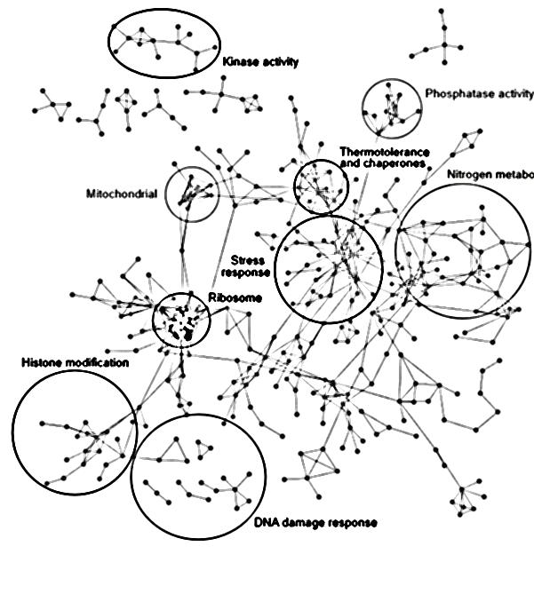
• Human susceptibility to environmental carcinogens is highly variable. This variability is partially due to genetics; however, genes that confer resistance are still unknown. Since many eukaryotic genes are conserved from yeast to humans, we used budding yeast to identify genes that confer resistance to carcinogens. We humanized the yeast barcoded deletion collection by introducing human genes that bioactivate carcinogens, and exposed yeast to 2-amino-3methylimidazo [4,5-f] quinoline (IQ), a heterocyclic aromatic amine linked to colon cancer. By high-throughput DNA sequencing of molecular barcodes, we identified genes that confer IQ resistance. Among the human genes orthologous to yeast resistance genes, the DNA repair genes hNTHL1 and RAD18 are risk factors for colon cancer. Future studies are to knockdown mammalian orthologs in cell cultures and determine subsequent IQ sensitivity.
• Expression of human CYP1B1, a cytochrome P450 gene expressed in the liver, breast, and prostate activates food carcinogens to become potent genotoxins in budding yeast.
• Among IQ resistance genes are those that participate in DNA damage tolerance, ribosome structure, histone modification, and ammonia metabolism. An interactome of gene functions is shown below.
• Perpetua, N., Kannan, A., Fasullo, M. CYP1B1 converts procarcinogens into genotoxins in Saccharomyces cerevisiae. Mutation Research, 874–875: 503440,2022.
• Fasullo M, Dolan M. The continuing evolution of barcode applications: Functional toxicology to cell lineage. Experimental Biology and Medicine. doi:10.1177/15353702221121600, 2022.
• Dolan, M, Zaidi, F., St. John, N., Doyle, F., Fasullo, M. High-throughput screening of the Saccharomyces cerevisiae genome for 2-amino-3-methylimidazo [4,5-f] quinoline resistance identifies colon cancer-associated genes. bioRxiv, Cold Spring Harbor Laboratory Press, 2022.
Acknowledgements
Funding: National Institutes of Environmental Health Sciences, R15 ES023685 Genome profiling of yeast resistance to heterocyclic aromatic amines
Collaborators: Francis Doyle (SUNY Polytechnic Institute) and Chris Vulpe (University of Florida)
Michael Fasullo
mfasullo@albany.edu
• The field of semiconductor nanowires (NWs) has become one of the most active research areas towards the realization of scalable on-chip devices. Progress is hindered due to the lack of development of novel scalable nanostructured materials and the ability to understand and control their properties at the nanoscale. The primary limiting fabrication challenge commonly faced, especially for feature sizes below 30 nm and bottom-up approaches, is the required deterministic (on-demand) and scalable integration, which involves control over the density, orientation, and spacing of the synthesized nanowires, parameters important for producing NWbased nanodevices.
• My group is focused on developing complementary metal-oxide-semiconductor (CMOS)-compatible fabrication strategies for nanostructured materials, for example, silicon carbide (SiC) and silicon oxycarbide NW arrays. These strategies enable the development of scalable ultrathin nanostructures, which can serve as an experimental platform to investigate NW-based emerging technologies, such as nanowire sensing/ optoelectronics, nanophotonics, and quantum photonics.
• Breakthrough: My group has demonstrated novel nanofabrication for sub-10 nm one-dimensional (1D) SiC NWs at predetermined locations, using CMOScompatible fabrication (recent publication in Nanomaterials with GlobalFoundries Corp.).
• This nanofabrication allows for self-aligned defectfree NWs to be fabricated without the use of a lithographic-pattern-transfer technique.


• Tabassum N., Kotha M., Kaushik V., Ford B., Dey S., Crawford E., Nikas V., and Gallis S*. On-demand CMOSCompatible Fabrication of Ultrathin Self-Aligned SiC Nanowire Arrays. Nanomaterials 8, 906 (2018).
• B. Ford, N. Tabassum, V. Nikas, S. Gallis*. Strong photoluminescence enhancement of silicon oxycarbide through defect engineering. Materials 10, 446 (2017).
• N. Tabassum, V. Nikas, B. Ford, M. Huang, A. E. Kaloyeros, S. Gallis*. Time-resolved analysis of the white photoluminescence from chemically synthesized SiCxOy thin films and nanowires. Appl. Phys. Lett. 109, 043104 (2016).
• National Science Foundation Grants No. ECCS-1842350.


Spyros Gallis (Spyridon Galis)
• The realization of scalable on-chip quantum devices requires novel nanostructured materials that must be high integrable and compatible with existing electronic circuits, waveguide architectures, and current chip-scale and silicon process technology. Non-classical (single-photon) light sources emitting in the near-infrared region of the electromagnetic spectrum, where signal transmission losses in optical fibers are small, are essential for the development of long-distance optical quantum networks.
• Single-photon emission at near-infrared wavelengths has been demonstrated in several systems. Nevertheless, none of them has exhibited the necessary and required properties, such as roomtemperature operation and photo-stable telecom Cband wavelength emission, radiative-limited excited state lifetimes, high photoluminescence (PL) efficiency, and compatibility with fab-friendly manufacturing technology, for practical telecom device implementation. These critical scientific and technological challenges have yet to be addressed. My research program focuses on filling these gaps and demonstrating scalable fab-friendly quantum photonic materials for the realization of chip-scale single-photon emitters.
• Breakthrough: We have introduced a new class of fab-friendly nanowire-based nanophotonic structures. These nanostructures enable the positioning of emitters - ions with an accuracy of 10 nm, an improvement on the current state-of-theart ion implantation processes, as reported in Nanophotonics1. Through a combination of correlation and comparison of temperaturedependence and time-resolved PL studies, my group has demonstrated a 22 times increase of the ioninduced emission in the nanophotonic structures, as compared to bulk devices, while using 20 times lower pumping power.

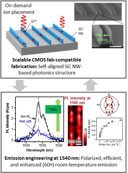
• Alex E. Kaloyeros, and Gallis S*. Polarization-dependent photoluminescence properties of fab-compatible nanowire-based nanophotonic structures. Appl. Phys. Lett. 120, 231104 (2022).
• 1Natasha Tabassum, Vasileios Nikas, Alex E. Kaloyeros, Vidya Kaushik, Edward Crawford, Mengbing Huang, and Gallis S*. Enhanced Telecom C-band Emission and Controlled Positioning of Er3+ by Scalable SiC Nanophotonic Structures. Nanophotonics, 9, 1425 (2020).
• Tabassum N., Kotha M., Kaushik V., Ford B., Dey S., Crawford E., Nikas V., and Gallis S*. On-demand CMOSCompatible Fabrication of Ultrathin Self-Aligned SiC Nanowire Arrays. Nanomaterials 8, 906 (2018).
• National Science Foundation Grants No. ECCS-1842350 and MPS-2130839. sgalis@albany.edu
Research - Galis Lab
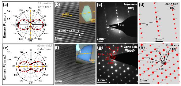
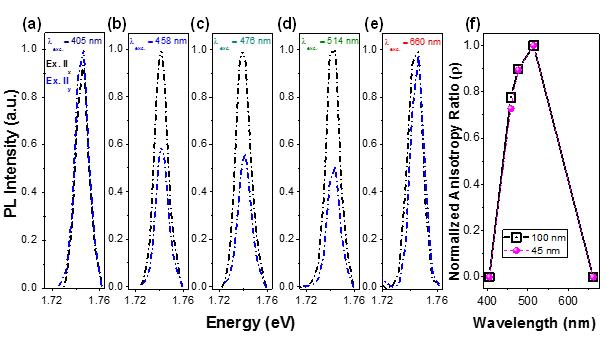
• Emerging 2D semiconductor materials, such as gallium telluride (GaTe), are promising layered semiconductors that can serve as vital building blocks towards the implementation of nanodevices in the fields of nanoelectronics, optoelectronics, and quantum photonics. Research in this program is focused on developing environmental-stable layered GaTe and on studying the anisotropy in the optical properties of GaTe nanomaterials and nanodevices. The polarization of reflected and emitted light can offer more details about an object or scene than traditional thermal or visible imaging. The polarization anisotropy is caused by the 1D-like nature of the GaTe layer, as the layer comprises of Ga-Ga chains extending along the b-axis crystal direction. The identification of the b-axis in such anisotropic materials is imperative for the fabrication of polarization-sensitive devices based on the generation and detection of polarized light, such as polarization-sensitive photodetectors and light sources.
• My group demonstrated an effective and novel encapsulation process using ultrathin hydrogen–silsesquioxane for environmental-stable GaTe flakes. This novel strategy provides a platform for studying the anisotropic properties of pristine GaTe flakes through polarization-resolved Raman and photoluminescence (PL) spectroscopies.
• Breakthrough: Polarization-resolved PL spectroscopy was used, in agreement with high-resolution transmission electron microscopy studies, to identify the b-axis crystal direction in capped GaTe flakes with various thicknesses. We observed polarization anisotropy contrast of ~0.6 at 532 nm for multilayer GaTe, which is comparable to other pseudo-1D materials like zirconium trisulfide.
Publications
• Mounika Kotha, Alex Kaloyeros, Thomas Murray, and Gallis S*. Wavelength-Dependent Anisotropic Optical Properties in Layered GaTe for Polarization-Sensitive Applications. Adv. Photonics Res. 2, 2100140 (2021).
• M. Kotha, T. Murray, D. Tuschel, and S. Gallis*. Study of Oxidation and Polarization-Dependent Optical Properties of Environmentally Stable Layered GaTe Using a Novel Passivation Approach. Nanomaterials 9, 1510 (2019).
• This work was partially supported by Gelest Inc.
• In collaboration with Lawrence Livermore National Laboratory (LLNL), we applied ion beam techniques to understand how nanoscale imperfections inhered from materials deposition and processing can impact the ability of dielectriccoated optical mirrors to resist high-power laser beams that are used in the National Ignition Facility for laser-induced inertial confinement nuclear fusion.
• With support from DARPA, we are working closely with our industrial partner to develop sapphire fiber based optical sensing capability for US hypersonic research programs.
• The work with LLNL identified structural imperfections like nanobubbles and nonstoichiometry in hafnia coatings as important mechanisms for laser damage. The findings provide a fundamental basis for the development of potential mitigation strategies required for the realization of laser damage resistant hafnia films.
• Our work demonstrated that ion beam technology is effective in creating optical cladding and single-mode light transmission in sapphire fibers, a critical step toward optics sensing in harsh environments.
Single-mode sapphire fiber for industrial and military applications
Publications
• P. B. Mirkarimi et. al., Optical Materials Express 12, 3365 (2022).
• V. N. Peters et. al., Journal of Applied Physics 130, 043103 (2021).
• Funding support from DOE/Lawrence Livermore National Laboratory
• Funding support from DARPA/OptoXense
mhuang@albany.edu
Nanoscale Visualization
• Electrostatic barriers at the interface between materials are the foundation of electronic and optoelectronic devices. Continued scaling below the sub -10-nm feature size is straining the ability to measure and control interface electrostatics and resulting device performance.
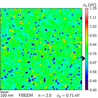
• The LaBella group has invented the ability to spatially resolve or visualize the electrostatic barrier at an interface between two materials to nanoscale dimensions. It utilizes a scanning tunneling microscopy (STM) technique called ballistic electron emission microscopy (BEEM). The STM tip is positioned on a regularly spaced grid with nanoscale resolution, where spectroscopy is utilized to measure the local electrostatic or Schottky barrier height as depicted.
• Computational modeling of the physics of the interface and electron transport has been developed that provides insight into the fundamental physical and chemical interactions occurring at the material interface. These interactions are the foundation of the barrier ’s spatial (non) uniformity
Nanoscale map of the electrostatic barrier at metal/HfOx interface. A large 1 eV variation is observed and attributed to film nonuniformity.
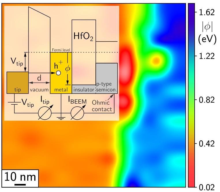
Mapping and computational modeling results of a non uniform interface, where multiple barrier heights are detected due to metal species intermixing.
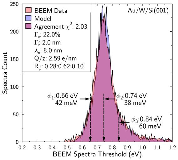
• Determination of the Energetic Resolution of Schottky Barrier Visualization via Interface Band Structure and Parallel Momentum Conservation,Jack Rogers, Westly Nolting, Chris Durcan, Robert Balsano, Vincent P. LaBella, AIP Advances, 11 025108 (2021).
Visualizing Metal/HfO2/SiO2/Si(001) Interface Electrostatic Barrier Heights with Ballistic Hole Emission Microscopy, Jack Rogers, Hyeonseon Choi, Steven Gassner, Westly Nolting, Daniel Pennock, Steven Consiglio, Vincent P. LaBella, Journal of Applied Physics, 126 195302 (2019).
• TEL America for providing HfO samples
• Carbon nanotube solar cell devices inspired by photosynthesis.
• Topological quantum computer to allow computation that scales faster than Moore’s law according to:
~e(Moore’s Law)
• Quantum transport modeling of ballistic nanoscale transistors.
• AI-specific hardware based on compact XNOR logic made using reconfigurable 2D transistors.
• Extensive use of our 300mm wafer line, including the integration of novel 2D materials in our line.
• The only US-based 300mm SOI radhard wafer development effort.
Publications
All-carbon nanotube tandem solar cell devices mimic the light excitation funneling process found in photosynthetic systems. Both systems transfer photogenerated excitons to their respective energy conversion “centers” as shown below.
1. Andreev Reflection and Klein Tunneling in High-Temperature Superconductor/Graphene Junctions, Sharadh Jois,1, ∗ Jose L. Lado,2, † Genda Gu,3 Qiang Li,3 and Ji Ung Lee, (In review)
2. Measuring the Electronic Bandgap of Carbon Nanotube Networks in Non-ideal p-n Diodes, Gideon Oyibo1, Thomas Barrett1, Sharadh Jois1, Jeffrey Blackburn2, Ji Ung Lee*1 (In review).
3. All-carbon nanotube solar cell devices mimic photosynthesis, Gideon Oyibo1, Thomas Barrett1, Sharadh Jois1, Jeffrey Blackburn2, Ji Ung Lee*1 Nano Letters, oi.org/10.1021/acs.nanolett.2c03544, (2022).
Acknowledgements
•Funding: NRL and SAMRI
•Collaborators: Brookhaven Nat Lab, Aalto University
Project Summary
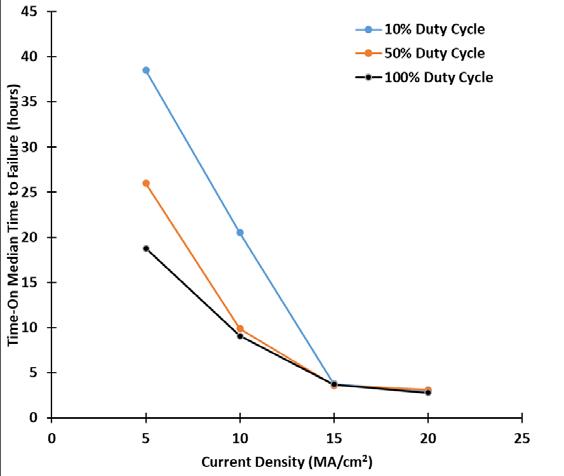
• Pulsed power electromigration was studied as a function of duty cycle and current density
• Significant relaxation observed at low current densities and little to no relaxation at higher current densities.
• Extrapolation of Pulsed Power Electromigration in engineering applications should take duty cycle of operation into consideration.
• Are these results repeatable at higher frequencies? The question remains unanswered.
Highlights
Publications
• Black’s Law in Light of Low Frequency Pulsed Power Electromigration
• Mohd Mueen Ul Islam Mattoo, SUNY Polytechnic Institute
• J. R. Lloyd, SUNY Polytechnic Institute
• Proceedings 2022 International Integrated Reliability Workshop
Acknowledgements
• CATN2 Funding
• GlobalFoundries support for samples
• Siemens (Mentor Graphics)
Jim Lloyd
• Using human Alkbh8Def cells and mice we will test the hypothesis that senescence occurs in vivo because of altered epitranscriptomic signals. Senescent cells adopt senescence-associated (SA) secretory phenotype (SASP), which includes the secretion of inflammatory cytokines, immune modulators, growth factors, and proteases, which together can damage or kill neighboring cells. We are testing the role of senescence in initially protecting epitranscriptomic deficient mice from detrimental redox-based signaling, but that the resultant SASP signaling promotes damage and stress to cause disease pathologies. The identification of senescent cells and their selective removal in vivo can be achieved using p16-3MR mice, which we have mated with Alkbh8Def mice.
Publications
• Melendez, J. A. The therapeutic bionanoscience interface. Exp Biol Med (Maywood). 2022 Dec 19:15353702221144090
• Lee, M. Y. et al. Selenoproteins and the senescence-associated epitranscriptome. Exp. Biol. Med. (Maywood). 15353702221116592 (2022)
• Huber, S. M. et al. Arsenite toxicity is regulated by queuine availability and oxidation-induced reprogramming of the human tRNA epitranscriptome. Proc. Natl. Acad. Sci. U. S. A. 119, e2123529119 (2022).
• Evke, S., Lin, Q., Melendez, J. A. & Begley, T. J. Epitranscriptomic Reprogramming Is Required to Prevent Stress and Damage from Acetaminophen. Genes (Basel). 13, (2022).
• National Cancer Institute
• National Institute of Environmental Health and Safety
• CATNMIP
• SUNY Poly Seed Award
• Begley & Tenenbaum and Nanobioscience labs jmelendez@albany.edu
J. Andres Melendez
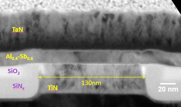
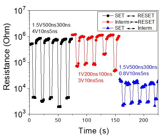
The project focuses on phase-change memory (PCM) materials as a likely candidate for multilevel/analog devices due to their internal property of resistance change and retaining that allows for programming and storage of synaptic weights and execution matrix-based computations in AI hardware.
Cross-sectional TEM image of Al0.4Sb0.6 PCM cell
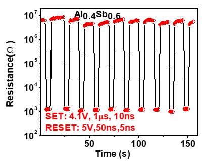
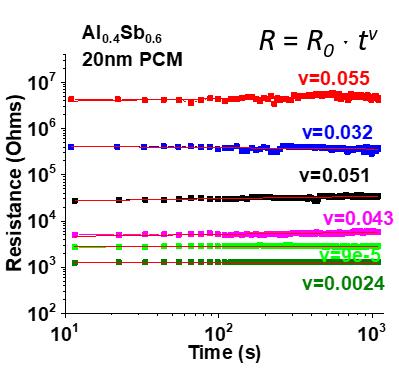
Extremely high (=5000) resistance contrast switching and low drift in 20nm thick Al0.4Sb0.6 cell
Publications
Three switching levels in doublelayer Ga0.2Sb/AlOx/Ga0.3Sb cell
1. R. Ume, et. al. Crystallization Properties of Al-Sb Alloys for Phase Change Memory Applications. ECS J. Solid State Science and Technology, 10(7), 075008 (2021).DOI: 10.1149/2162-8777/ac14dd.
2. H. Gong, et.al. "Bilayer Ga-Sb Phase Change Memory with Intermediate Resistance State." Device Research Conference (DRC) Extended Abstracts, pp. 1-2. IEEE, 2021. DOI: 10.1109/DRC52342.2021.9467153.
3. R. Ume, et.al. , "Electrical and structural properties of binary Ga–Sb phase change memory alloys," Journal of Applied Physics, vol. 132, p. 035103, 2022. DOI: 10.1063/5.0096022.
• Key collaborators: K. Beckmann (SUNY Poly), N. Cady (SUNY Poly), K. Brew (IBM), G. Cohen (IBM)
• Funding SUNY-IBM AI Collaborative Research Alliance
Serge Oktyabrsky
Attributes of recognized objects in IR
Publications
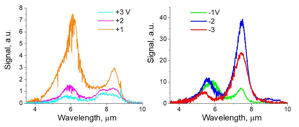
Quantum Well Infrared Photodetector (QWIP)
Band structure of QWIP period
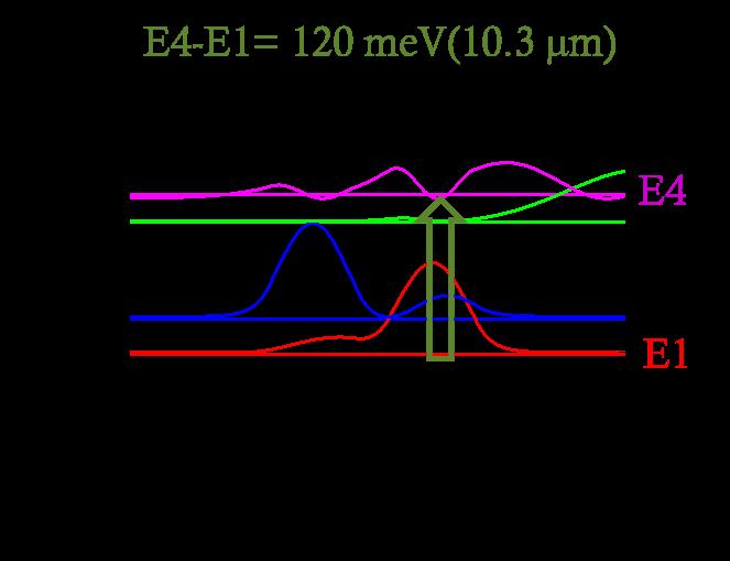
FTIR spectra: Bias-controlled IR sensitivity:
1. V. Mitin, S. Tulyakov, G. Biswal, M. Yakimov, V. Tokranov, and S. Oktyabrsky, “Tunable infrared detector for object recognition,” in Workshop on Innovative Nanoscale Devices and Systems, Book of Abstracts, ed. J.Fabian et al., 2022, p. 122-123.
2. G. Biswal, M. Yakimov, V. Tokranov, S. Tulyakov, V. Mitin, and S. Oktyabrsky. “Development of Voltage-Tunable IR Photodetector.” American Vacuum Society Hudson-Mohawk 2022 Fall Meeting, 2022, Albany, NY , Abstracts, p.12.
• Key collaborators: V. Mitin (SUNY Buffalo), S. Tulyakov, (SUNY Buffalo).
• Funding Army Research Office (ARO).
A joint project with U. Buffalo - SUNY focuses on the development, implementation and testing of an autonomous object recognition system that comprises of adaptable detectors/sensors driven by an artificial intelligence. The research focus is two-fold: (a) design and build a unique AI object recognition system with integrated IR wide band adaptive sensors (3-12 mm) based on asymmetrically doped doublequantum-well structures; and (b) exploration of the properties and potential benefits of the adaptive IR spectral sensitivity selection in changing environment. Serge Oktyabrsky
soktyabrsky@albany.edu
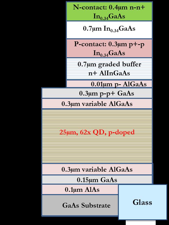
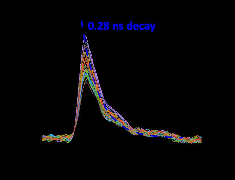
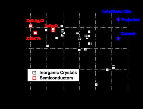
The project focuses on development of ultrafast high light yield scintillating detectors consisting of a quantum dot waveguiding medium with integrated wavelength-matched photodetector (PD) as an enabling technology for multiple highenergy physics applications, as well as for medical imaging and security purposes.
Structure of integrated QD scintillation detector
Ultrafast decay from 4.5MeV alpha-particles
Comparison of light yield and decay time of scintillators
Charge histograms for 4.5MeV alphaparticles with PDs of two sizes
1. V. Mitin, S. Tulyakov, G. Biswal, M. Yakimov, V. Tokranov, and S. Oktyabrsky, “Tunable infrared detector for object recognition,” in Workshop on Innovative Nanoscale Devices and Systems, Book of Abstracts, ed. J.Fabian et al., 2022, p. 122-123.
2. A. Minns, K. Dropiewski , M. Yakimov, V. Tokranov, M. Hedges and P. Murat, and S. Oktyabrsky, “Parameters of Fast and High-Yield InAs/GaAs Quantum Dot Semiconductor Scintillator,” MRS Advances 2021, DOI: 10.1557/s43580021-00019-y.
3. Acknowledgements
• Key collaborators: P. Murat (Fermilab), M. Hedges (Purdue).
• Funding: DOE, NSF
Serge Oktyabrsky
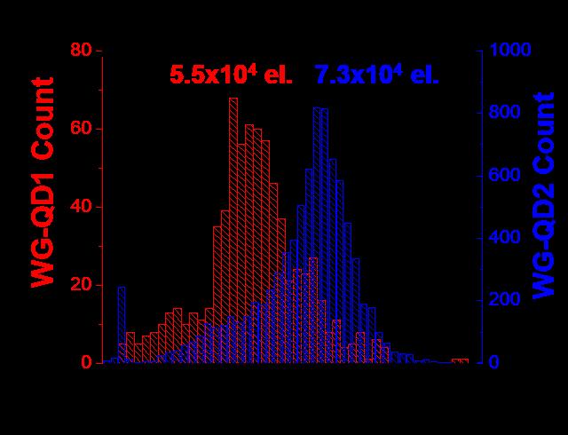
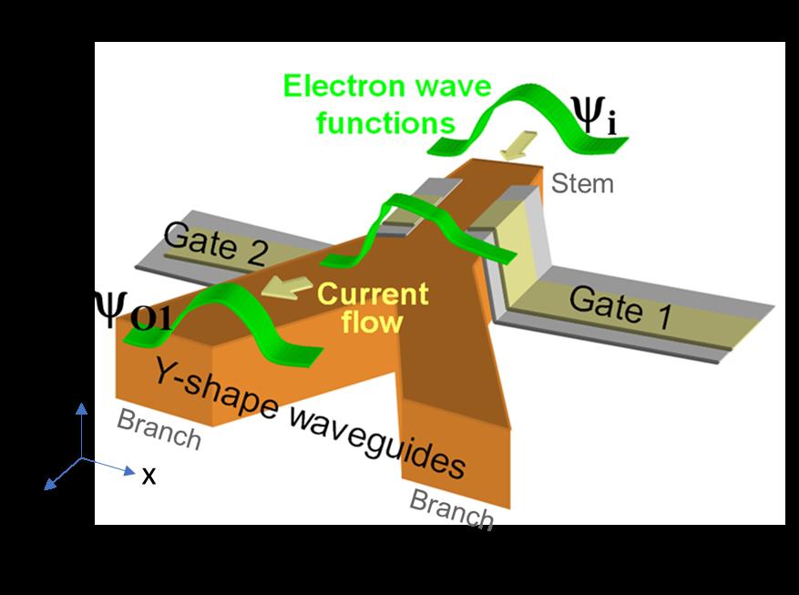
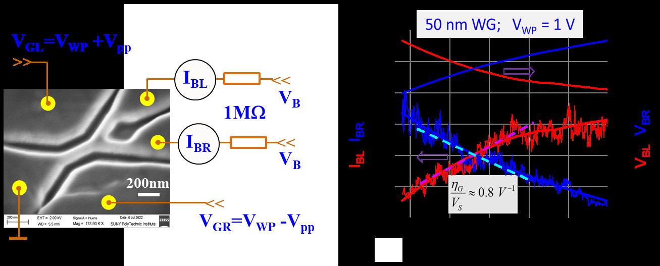
A joint project with U. Buffalo is focused on the development of principles and technologies for a direct manipulation of electron quantum states in semiconductor ballistic waveguides by applied electrostatic potential. The technical approach relies on a specially designed nanoscale semiconductor structure where electrons travel as one-dimensional waves, and high-efficiency gate electrodes control the electron wave propagation in Y-shaped branching waveguides.
Simulation of electron concentration (Left plots) and current density (Right plots) for YBS with 5 × 1010 cm 2 doping, VG= 12 mV, VDS=1mV, T=77K
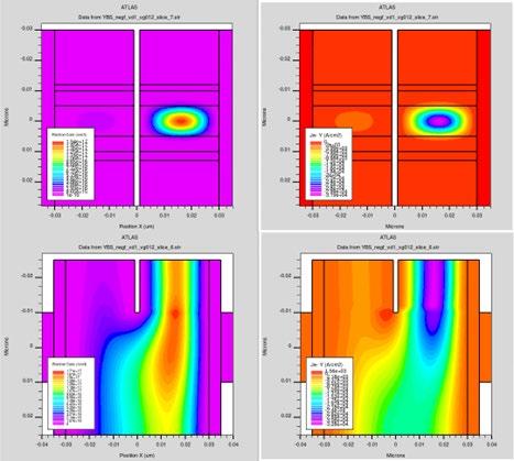
Schematic diagram of a Y-branch switch with MOS gates in operation
SEM image, schematics and 77K YBS characteristics of the ballistic YBS characteristic
1. T. McDonough, V. Mitin, V. Tokranov, M. Yakimov, and Serge Oktyabrsky, “Quantum switching modeling and optimization of a metal-oxide-semiconductor gated Y-shaped structure,” NanoWorld Journal, 2021. DOI: 10.17756/nwj.2021-089.
2. V. Mitin, T. McDonough, M. Yakimov, V. Tokranov, and S. Oktyabrsky, “Switching based on a onedimensional electron gas in a Y-shaped device,” in Workshop on Innovative Nanoscale Devices and Systems, Book of Abstracts, ed. J.Fabian et al., 2022, p. 23-24.
• Key collaborators: V. Mitin (SUNY Buffalo).
• Funded by Air Force Office of Scientific Research (AFOSR)
soktyabrsky@albany.edu
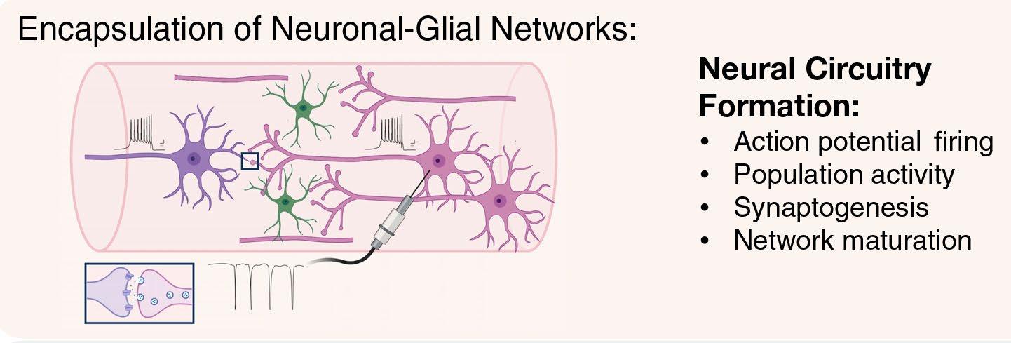
• Multiscale models of neurons at the level of synapses, dendrite or axon functions, and spatial neuronal networks are being developed as custom integrated software-custom hardware platforms (collaboration Dr. Mukherjee, Amrita Univ).
• SyNC- neural net for synaptic plasticity modeling of complex synaptopathies (Autisms) and patientspecific drug treatment interactions (patented).
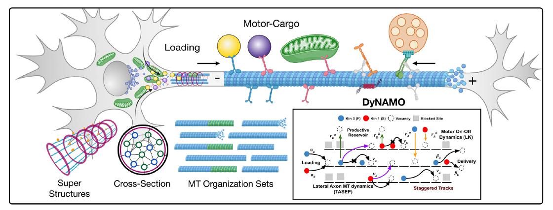
• DyNAMO- theoretical axon for axonopathies arising from Traumatic Brain Injury.
• NEMo- dendrite to axon nanocommunication network for modeling amyloid beta perturbation of receptors, membranes, calcium signaling, and axonal transport in Alzheimer ’s disease.
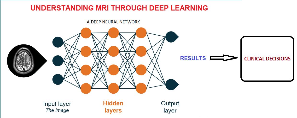
• SCENIC derivations- CNN Deep Learning diagnostics for brain tumor detection and typing (glioblastoma vs metastasized tumors)of MRI clinical modalities (collaborator Dr. Julie Pilitsis, M.D. Ph.D.).
• Other: spatial multi-synaptic, multi-neuron type signaling; dendritic trees; brain vascular mapping.
Publications
• Z.T. S.F. Bush, J.L. Paluh, G. Piro, V. Rao, V. Prasad, A. Eckford, et al. (2015) P1906.1TM-2015 Recommended Practice for Nanoscale and Molecular Communication Framework. IEEE Standard 1906.1TM-2015. ISBN: 978-1-5044-01-1-2
• S.F. Bush, G. Mantelet, J.L. Paluh, et al. (2020) IEEE Standard Data Model for Nanoscale Communication Systems. IEEE Standard 1906.1.1TM-2020. ISBN: 978-1-5044-6994-4
• A. Banerjee, J.L. Paluh, A. Mukherjee, K.Gaurav Kumar, A. Ghosh, M.K. Naskar (2018) Modeling the neuron as a nanocommunication system to identify spatiotemporal molecular events in neurodegenerative disease. Intern. J. Nanomed. 13: 3105-3128. dx.doi.org/10.2147/IJN.S152664
• R. Chatterjee, J.L. Paluh, S. Chowdhury, S. Mondal, A. Raha, A. Mukherjee (2021) SyNC, a computationally extensive and realistic neural net to identify relative impacts of synaptopathy mechanisms on glutamatergic neurons and their networks in Autism and complex neurological disorders. Frontiers in Cellular Neuroscience. 15:674030. doi: 10.3389/fncel.2021.674030
• B. Sai T. Naidu, S. Biswas, R. Chatterjee, S. Mandal, S. Pratihar, A. Chatterjee, A. Raha, A. Mukherjee and J.L. Paluh (2022) SCENIC: An area and energy-efficient CNN-based hardware accelerator for discernable classification of brain pathologies using MRI. VLSI Design Conference.
Acknowledgements
• SUNY Polytechnic and SUNY RF internal funds; ITrakNeuro Start-Up
Janet L. Paluh, Ph.D.
jpaluh@albany.edu
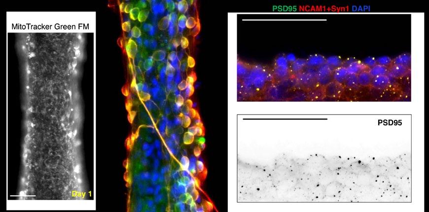
• Spinal Cord Injury (SCI) that results in loss of neurons in patients remains untreatable. Human stem cell neurotechnologies now allow regional matching of neurons that is coupled with single cell RNA-Seq for molecular and spatial diagnostics to accelerate bench to clinic therapeutics In a first of its kind series of studies, research from the Paluh lab that preforms and transplants neuronal circuits in animal models is being done to replace lost spinal neuron connectivity
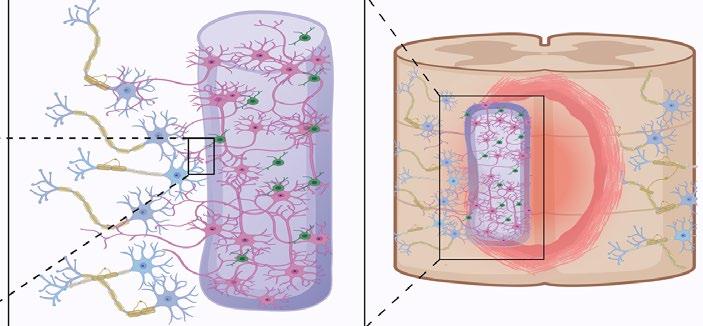
• Recent discoveries in mammalian development identify bifurcating pathways for neurodevelopment of the brain and spine, with the latter requiring neuromesodermal progenitors (NMPs) The ability to match neuron identities regionally via stem cell neurotechnologies now allows direct in vivo therapeutics with neurons, for brain Parkinson’s or rapidly integrating circuits for spinal trauma.
• Central and peripheral nervous systems (CNS, PNS) interconnect in networks from the spine. The Paluh lab use of NMPs has enabled the first CNS-PNS integrated models of the primitive gut and heart (patented), also benefiting organ biomanufacturing
• Z.T. Olmsted and J.L. Paluh (2021b) Stem cell neurodevelopmental solutions for restorative treatments of the human trunk and spine. Frontiers Cell Neurosci. 15:667590. doi: 10.3389/fncel.2021.667590
• M. B. Paredes-Espinosa and J.L. Paluh (2022) Human stem cell derived neurons and neural circuitry therapeutics: Nest frontier in spinal cord injury repair. Experimental Biology and Medicine. doi: 10.1177/15353702221114099
• Z.T. Olmsted, C. Stigliano, A. Scimemi, T. Wolfe, J. Cibelli, P.J. Horner, and J.L. Paluh (2021c) Transplantable human motor networks as a neuron-directed strategy for spinal cord injury. iScience. 24:102827. doi: 10.1016/j.isci.2021.102827.
• Z.T. Olmsted and J.L. Paluh (2021a) Co-development of central and peripheral neurons with trunk mesendoderm in human elongating multi-lineage organized gastruloids. Nature Communications 12:3020. doi: 10.1038/s41467-02123294-7
• Z.T. Olmsted and J.L. Paluh (2022) A combined human gastruloid model of cardiogenesis and neurogenesis. iScience. 25:104486. doi: 10.1016/j.isci.2022.104486
• NYSTEM, NYSCIRB, SUNY Polytechnic SEED, CATN2 MIP
Janet L. Paluh, Ph.D.
jpaluh@albany.edu
1. Automation, Productivity and Innovation in Information Technology
This research develops a theoretical model to study the impact of innovations in Information Technology (IT) on automation, productivity growth and employment, and how increasing automation of production in turn affects the rate of innovation in IT.
2. Market Structure in Technology Industries
This research re-examines an old question in industrial organization – what determines whether a firm decides to make a component or tool in-house or buy it from an external supplier? The project studies this in the context of a technologically intensive input that has a wide variety of use, like semiconductor chips.
3. Diffusion of Information Technology
This project uses data from U.S Input-Out Tables to understand the pattern of diffusion of semiconductor chips, computer hardware and software across different sectors in the economy.
Publications
Highlights
• Even if innovations in IT leads to increasing automation in every firm, it is possible to have total employment in the economy increase over time, as innovations lead to reduction in production costs, and entry of new products which require labor in production.
• The model developed in the research can explain why different parts of the semiconductor chip supply chain show different evolutions in the make or buy decision.
1. Automation, Productivity and Innovation in Information Technology, Unni Pillai, Macroeconomic Dynamics, 2022.
2. Diversity of Input Use and R&D Outsourcing, Unni Pillai, In Review (Journal of Economic Management and Strategy)
Acknowledgements
• SUNY Poly Seed Grant
Low p-type doping efficiency is a perennial issue in IIInitride material and device development. This is largely because the only currently viable p-type dopant in the material system, Mg, is a deep acceptor, ~160 meV above the GaN valence band maximum (VBM). Be has a shallower acceptor level, ~113 meV above the GaN VBM, but to date, no reliable or reproducible p-GaN:Be has been shown. However, metal-organic chemical vapor deposition (MOCVD) has been largely underutilized in GaN:Be research until our recent work.
As part of our development of in situ Be doping during MOCVD growth of GaN, we explored a large parametric space of growth variables Through these studies, we are able to control Be concentration up to technologically-relevant values of ~1019 cm-3 with smooth 2D surface morphology, which is essential for device fabrication.
We also developed a novel “pulsed growth” method, wherein Be precursor is pulsed into the growth chamber separately from nitrogen and gallium precursors to reduce gas-phase parasitic reactions. This results in both elevated Be concentration and highly controllable growth rate.
Publications
B. McEwen, M. A. Reshchikov, E. Rocco, V. Meyers, K. Hogan, O. Andrieiev, M. Vorobiov, D. O. Demchenko, and F. Shahedipour-Sandvik, ACS Applied Electronic Materials 4 (8), 3780-3785 (2022). DOI: 10.1021/acsaelm.1c01276
B. McEwen, M. Reshchikov, E. Rocco, V. Meyers, K. Hogan, O. Andrieiev, M. Vorobiov, D. Demchenko, and S. Shahedipour-Sandvik "Toward highly efficient p-doping in IIInitride optoelectronics: MOCVD growth of Be-doped GaN", SPIE Photonics West (2022). https://doi.org/10.1117/12.2626491
Acknowledgements
• NSF (funding agency)
• Prof. Michael A. Reshchikov (VCU)
sshahedipour-sandvik@albany.edu
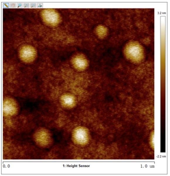
Promising the possibility of obtaining p-type GaN from Be doping, we find the presence of a UVLBe band, which confirms the presence of the predicted shallow acceptor state in MOCVD GaN:Be. Unknown acceptor compensation is suggested by the YLBe band, however. An atomic force microscope image is shown right, showing high-quality smooth 2D growth mode.

M. A. Reshchikov, O. Andrieiev, M. Vorobiov, D. Ye, D. O. Demchenko, K. Sierakowski, M. Bockowski, B. McEwen, V. Meyers, and F. Shahedipour-Sandvik, Thermal annealing of GaN implanted with Be, Journal of Applied Physics 131, 125704 (2022). https://doi.org/10.1063/5.0080060
M. A. Reshchikov, M. Vorobiov, O. Andrieiev, B. McEwen, E. Rocco, V. Meyers, D. O. Demchenko, and F. S. ShahedipourSandvik, Photoluminescence from Be-Doped GaN Grown by Metal-Organic Chemical Vapor Deposition, Phys. Status Solidi B 2200487 (2023). https://doi.org/10.1002/pssb.202200487
• Prof. Denis O. Demchenko (VCU)
P-type doping of GaN presents distinct challenges for power electronics, LEDs, and sensors. The prevailing p-type dopant, Mg, can be introduced by implantation cheaply and controllably. However, implantation creates defects that must be removed at very high temperatures before a p-type film is possible. By the novel employment of a gyrotron microwave source (in collaboration with Gyrotron Technology Inc.), a wafer of GaN can be annealed in short (<2 s) ‘pulses’ at temperatures of 1450 °C (2640 °F) to achieve ptype activation of Mg-implanted GaN without significant surface degradation. We study the creation, evolution, and redistribution of defect and dopant states to understand how they respond to this ultra-hot annealing. In turn, this gives us insight into how better power electronics can be engineered. Extensive use of CNSE metrology facilities and clean room enables material characterization and device fabrication.
Meyers, V., et al. "P-type conductivity and suppression of green luminescence in Mg/N co-implanted GaN by gyrotron microwave annealing." J. of Appl. Phys. 130.8 (2021)
Meyers, V., et al. "Defect-mediated diffusion of implanted Mg in GaN: suppressing dopant redistribution by sequential thermal and microwave annealing J. of Appl. Phys. (in review)
• ARPA-E PNDIODES program, direction of Isik Kisilyalli
• Mike Shevelev and Vlad Sklyar (Gyrotron Technology Inc.)
Distortion of an implanted dopant profile due to diffusion during annealing can be reduced 10-fold through a 2-stage anneal.
This works by removing some crystalline damage at a moderate temperature (1000 °C) before activating dopants at a high temperature (1450 °C).
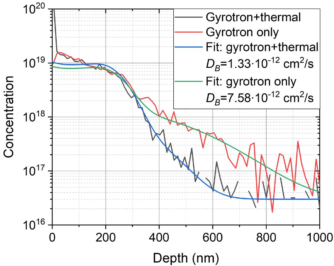
Shahedipour-Sandvik, Shadi, et al. "Defect Microstructural Evolution of Co-Implanted and Gyrotron Microwave-Annealed GaN." Meeting of the Electrochemical Society. Delivered virtually, 2021.
• Prof. Mark Goorsky (UCLA)
• Prof. Rachel Goldman (U. Mich.)
• Prof. Mike Dudley (SUNY Stony Brook)
We are developing optical detectors that work in the infrared based on GaN/AlGaN superlattice structures called QWIPs (quantum well infrared photodetectors). This is possible by taking advantage of shallow quantum wells created by the superlattice, causing longwavelength light to absorb in material that has a band gap so large that it normally absorbs only ultraviolet light
Combining quantum-mechanical and classical simulations of GaN/AlGaN band structures in collaboration with SRI International enables us to tune the absorption spectrum of these structures Metalorganic chemical vapor deposition (MOCVD) is used to grow the superlattice structures monolayer-bymonolayer to achieve nm-scale controllability of film thickness.
By utilizing pulsed introduction of GaN precursors in an MOCVD reactor, highly controllable growth rate (similar to atomic layer deposition) can be achieved from a typically rapid (>2 μm/hr) growth method.
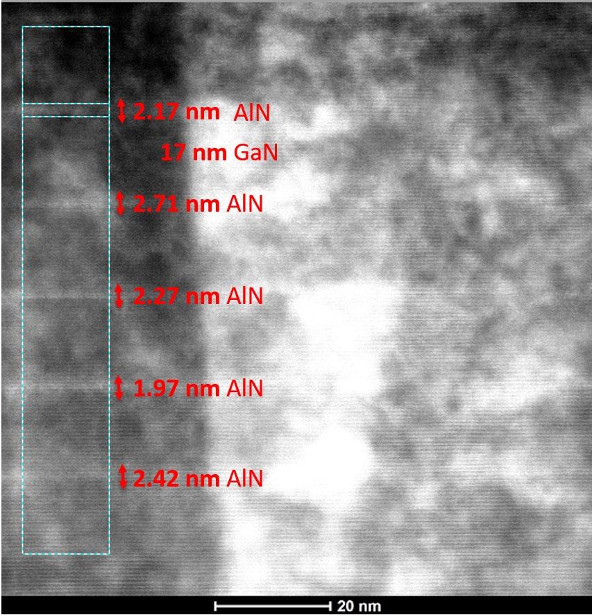
• DARPA (funding agency)
• David Hill and Winston Chan (SRI International)
• Dr. Thomas Murray (SUNY Poly metrology)
Shadi Shahedipour-Sandvik
The WBG-Optronix Laboratory continues an ongoing research program on the development of high-efficiency, airstable III-nitride photocathodes. Photocathodes have applications in photon detection for astronomy, communications, and image intensifiers. Additionally, photocathodes are used in high-energy physics applications as high-brightness electron sources.
Recent studies have focused on improving device efficiency by optimizing the electrostatic profile The role of planes on Mg p-type dopant incorporation has been investigated through MOCVD selective area growth (SAG) of microstructures with polar, semi-polar and non-polar facets along Ga- and N-polar directions Mg-incorporation in the various planes and the impact on photocathode device efficiency have been studied via optical and electrical measurements Control of unintentional impurity profiles has also been studied by secondary ion mass spectrometry (SIMS) Oxygen impurities are found to incorporate at interfaces and diffuse through bulk and defect mediated pathways based on process parameters
Surface stabilization of photocathodes has also been investigated. Wet chemical treatments have been used to remove surface contaminants and increase device efficiency. We have also investigated 2-D materials including graphene and hexagonal boron nitride (h-BN) to fully stabilize the IIInitride surface.
Publications
E. Rocco, J. Marini, K. Hogan, V. Meyers, B. McEwen, L.D. Bell, and F. Shahedipour-Sandvik, Overview and Progress Toward High-Efficiency, Air-Stable Photocathode Detectors. (2022) IEEE Photonics Journal, vol. 14, no. 2, pp. 1-12. https://doi.org/10.1109/JPHOT.2022.3155383
L. Cultrera, E. Rocco, F. Shahedipour-Sandvik, L.D. Bell, J.K. Bae, I.V. Bazarov, P.Saha, S. Karkare, and A. Arjunan, Photoemission characterization of N-polar III-nitride photocathodes as candidate bright electron beam sources for accelerator applications. (2022) Journal of Applied Physics, vol. 131, 124902. https://doi.org/10.1063/5.0076488
Shown below, SEM micrographs of Ga-polar microstructure grown SAG in MOCVD with polar and semi-polar facets, and subsequent overgrowth of GaN:Mg layers. The resulting structure was characterized by microphotoluminescence mapping. We observe increased intensity of the UVLMg band - associated with high p-type conductivity - on the semi-polar facets.
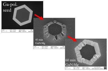
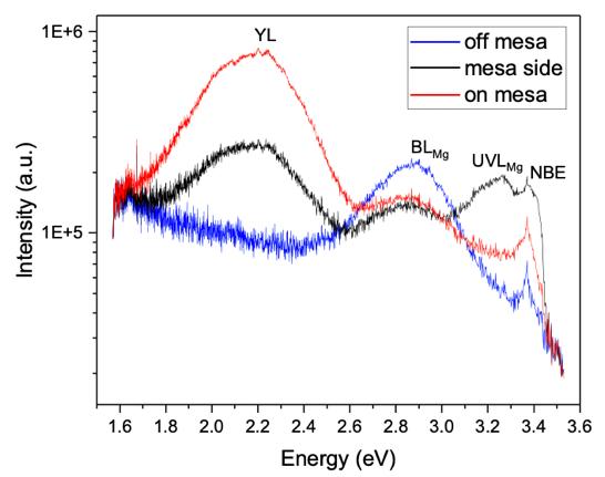
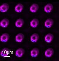

E. Rocco, I. Mahaboob, K. Hogan, V. Meyers, B. McEwen, L.D. Bell, and F. Shahedipour-Sandvik. Impurity incorporation and diffusion from regrowth interfaces in N-polar GaN photocathodes and the impact on quantum efficiency. (2021) Journal of Applied Physics, vol. 129, 195701.
https://doi.org/10.1063/5.0049344
Acknowledgements: National Aeronautics and Space, Administration (NASA), U.S. Department of Energy (DOE)
The objective of this Future Manufacturing project is to develop novel manufacturing technologies for production of hybrid bioelectronic and biophotonic devices. The specific questions to be addressed are: 1) How do we design and manufacture electronic and photonic devices that are biocompatible (i.e., facilitate growth and function of healthy biological tissues) and are bio-resilient (i.e., able to withstand the wet, salty, proteinaceous chemical environment of biological systems) while permitting information transfer either electronically or using integrated photonics? 2) How will we interface different tissues with devices in a manner that provides overlap to facilitate scalable manufacturing?
Research in this seed grant focuses on design and manufacturing of silicon-wafer electronic and photonic devices applied to the following testbeds: 1) Implementation of a pressure sensing device that can measure outflow from ocular tissues to address development of glaucoma therapeutics; 2) Creation of multielectrode arrays interfaced with three-dimensional cell cultures (e.g., neuronal organoids) for electrical stimulation and observation.
In addition, we will develop an extensive workforce training program stretching from community college to doctoral students.
Publications
• NIH 3T3 fibroblasts and neural stem cells have been cultured on silicon wafers coated with a variety of different metals routinely used in semiconductor technologies.
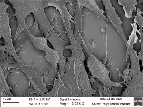
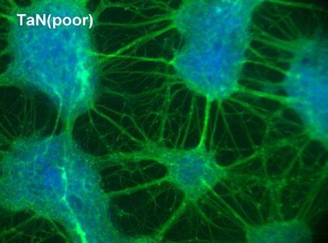
Left panel: SEM of NIH3T3 cells on aluminum-coated wafers; right panel: fluorescent micrograph of neural stem cells grown on tantalum nitride-coated wafers.
• Photonic chips have been designed to investigate the effects of cell growth on light propagation in waveguides, Mach-Zehnder interferometers, ring resonators, and Bragg gratings
• Outreach activities were held with students from Questar New Visions and SUNY Poly Utica campus
• S.T. Sharfstein, Bio-hybrid electronic and photonic devices, experimental Biology and Medicine, in press.
doi: 10.1177/15353702221144087
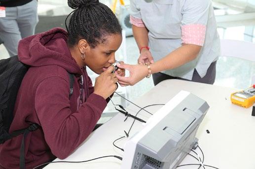
• Academic collaborators: Yubing Xie, Nate Cady, Natalya Tokranova, Nick Fahrenkopf, Karsten Beckmann
• AIM Photonics, NYCREATES, Neural Stem Cell Institute
• NSF ECCS- 2134518
Susan Sharfstein
• This project focuses on development of a novel, low-shear, high mass-transfer bioreactor for automated expansion and recovery of hematopoietic cells and stem cells for therapeutic applications, including immuno-oncology. Proof of principle experiments will employ Jurkat cells as a model T cell line and induced pluripotent stem cells (iPSCs) differentiated down the pancreatic lineage. Novel cell removal strategies include thermo-responsive polymers to reduce cell damage upon removal from the matrix.
• Matrix materials under consideration include cellulose and 3D printed poly-lactic acid (PLA)
• In parallel with academic studies optimizing culture conditions for cell growth and recovery, our industrial partner, Sepragen (owner of the bioreactor technology), is focused on development of a closed, automated system to translate the technology into a commercial product for deployment in the cell therapy market.
• Studies with iPSCs differentiated down the pancreatic lineage, demonstrated our ability to obtain insulin producing cells in the novel bioreactor with a cellulose matrix.
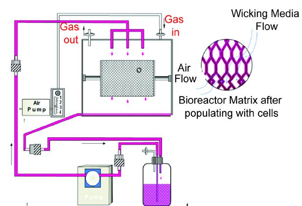
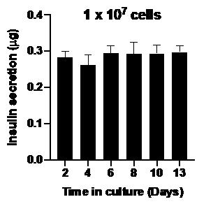
• In contrast, Jurkat cells grew poorly on the cellulose matrix, but performed much better on the PLA matrix (shown in the black box below).
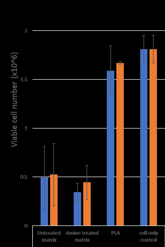
• Current studies are focused on improving adhesion to the matrix by coupling thermoresponsive polymers to the PLA.
• N. Amini, J.L. Paluh, Y. Xie, V. Saxena, and S.T. Sharfstein, Insulin production from hiPSC-derived pancreatic cells in a novel wicking matrix bioreactor, Biotechnology and Bioengineering, 117: 2247-2261 (2020) doi: 10.1002/bit.27359
• Novel Bioreactors for Therapeutic Cell Expansion: Regenerative Medicine and Immuno-oncology Applications, Keynotion Global Bioprocessing Summit, San Francisco, CA, November 2022
• Academic collaborators: Yubing Xie, Jan Paluh. Industrial collaborators: Sepragen Corporation, Merck & Co., Genentech
• NSF IIP-1722384
• This work was partially performed under a Project Award Agreement from the National Institute for Innovation in Manufacturing Biopharmaceuticals (NIIMBL) and financial assistance award 70NANB17H002 from the U.S. Department of Commerce, National Institute of Standards and Technology.
Susan Sharfstein
• The objective of this project is to create a competitively priced bioengineered heparin produced by murine mastocytoma cells cultured in bioreactors as an alternative to the currently available animal-derived heparin, which is primarily sourced from pig intestines harvested in China.
• Metabolic engineering was performed by our collaborators at TEGA Therapeutics to optimize the composition and anticoagulant activity of the mastocytoma derived heparin. The focus of activities at SUNY Poly is to improve productivity by increasing the maximum cell density for cells grown in stirred tank bioreactors and to determine whether the specific productivity can be improved by optimizing medium formulation and bioprocess conditions.
• Media formulation significantly affects viable and integrated viable cell density (IVCD)
• Bioreactor experiments demonstrated significant shear sensitivity, which was alleviated by increasing the Pluronic F68 concentration. Aeration required optimization to provided adequate oxygen without increased shear.
Publications
• B.E. Thacker, K. J. Thorne, C. Cartwright, J.Park, K. Glass, A. Chea, B. P. Kellman, N. E. Lewis, Z. Wang, A. Di Nardo, S.T. Sharfstein, W. Jeske, J. Walenga, J. Hogwood, E. Gray, B. Mulloy, J. D. Esko, C.A. Glass, Multiplex genome editing of mammalian cells for producing recombinant heparin, Metabolic Engineering, 70: 155-165 (2022) doi: 10.1016/j.ymben.2022.01.002
• B.E. Thacker and S.T. Sharfstein, Metabolic Engineering of Mammalian Cells to Produce Heparan Sulfates, Emerging Topics in Life Sciences, 2 (3) 443-452 (2018) DOI: 10.1042/ETLS20180007
• Center for Biopharmaceutical Education and Training, Albany College of Pharmacy and Health Sciences
• TEGA Therapeutics
• NIH 1R01GM090127; NSF IIP-1321432, IIP-1622959, IIP-1842736, IIP-2026188
Susan Sharfstein
• Currently, SiC MOSFETs are fabricated using elevated temperature (≥ 500ᴼ C) aluminum implantation for the formation p-doped regions to prevent the introduction Basal Plane Dislocations (BPDs) during the activation anneal Switching to room temperature (RT) implantation of aluminum would decrease the overall processing complexity and cost. However, when RT implantation is performed, it is common for BPDs to be introduced from implantation damage and activation anneal processes These BPDs degrade the performance and reliability of MOSFETs and other SiC devices.
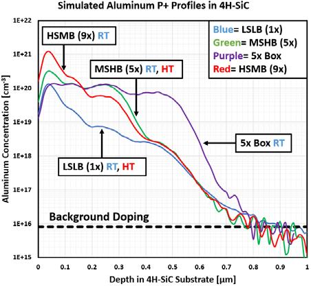
• Previously, a critical aluminum dose of 1x1015cm-2 was reported to prevent significant BPD generation while utilizing room temperature ion implantation however, with proper control over the implantation energy and dose altogether (i.e., the profile) devices with an implant dose nearly 10x greater than the previous critical dose can be fabricated while simultaneously suppressing BPD generation and thus improving device performance and longevity.
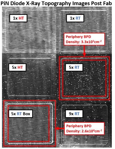
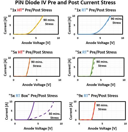
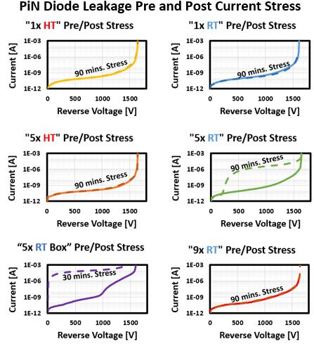
• S. A. Mancini, S. Y. Jang, D. Kim and W. Sung, "Increased 3rd Quadrant Current Handling Capability of 1.2kV 4H-SiC JBS DiodeIntegrated MOSFETs (JBSFETs) with Minimal Impact on the Forward Conduction and Blocking Performances," 2021 IEEE 8th Workshop on Wide Bandgap Power Devices and Applications (WiPDA), 2021, pp. 101-106, doi: 10.1109/WiPDA49284.2021.9645152.
• S. A. Mancini et al., "Static Performance and Reliability of 4H-SiC Diodes with P+ Regions Formed by Various Profiles and Temperatures," 2022 IEEE International Reliability Physics Symposium (IRPS), 2022, pp. P62-1-P62-6, doi: 10.1109/IRPS48227.2022.9764538.
• S. A. Mancini, S. Yup Jang, D. Kim and W. Sung, "Exploring Optimum Designs for 1.2kV 4H-SiC JBS Diode Integrated MOSFETs (JBSFETs)," 2022 IEEE 9th Workshop on Wide Bandgap Power Devices & Applications (WiPDA), 2022, pp. 11-16, doi: 10.1109/WiPDA56483.2022.9955290.
• S. A. Mancini et al “Investigation of 1.2kV 4H-SiC MOSFET Static Performances Fabricated Utilizing All Room Temperature Ion Implantation,” to be submitted to IEEE Transaction on Electron Devices.
• S. A. Mancini et al., “Design and Cell Layout in 4H-SiC MOSFETs to Provide Long Term Reliability Even in the Presence of Basal Plane Dislocations,” to be submitted to IEEE Transaction on Electron Devices.
• This work was supported by the National Renewable Energy Laboratory (“NREL”), U.S. Department of Energy, the Advanced Manufacturing Office, DE-AC36-08GO28308.
Manufacturing
• There is an urgent need to create a source of domestic high voltage devices and modules to encourage lower prices and help the adoption of high voltage devices for steady state and pulse power applications.
• Many commercial applications such as variable speed drives for MW class electric motors, 13.8 kV distribution grid equipment, incorporation of renewables on the distribution grid and High Voltage DC (HVDC) transmission will benefit from these devices.
• The MUSiC team proposes to develop a baseline process to fabricate state-ofthe-art 20+ kV SiC PiN diodes, MOSFETs, IGBTs.
Publications
• Development of state-of-the-art High Voltage (HV), >15kV rated 4H-SiC MOSFETs
• Established a baseline process for fabrication of Ultra-HV (20kV) rated devices at a leading foundry company located in the U.S
• Developed and demonstration of custom Ultra-HV packages for use in high voltage applications
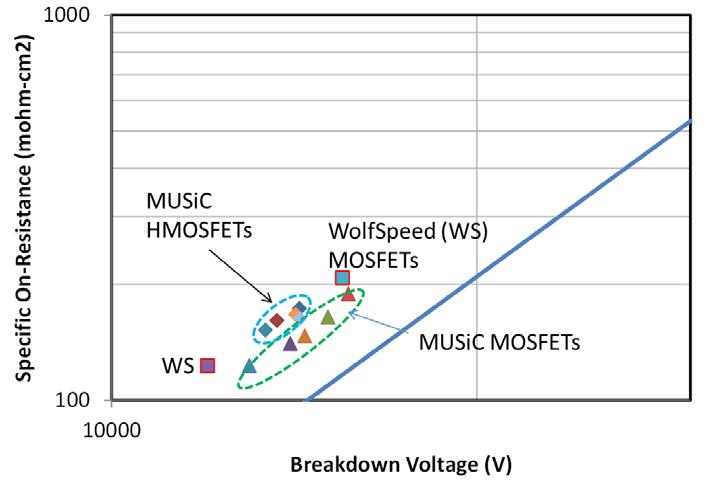
Fig. 1. Ron,sp – BV trade-off achieved in Phase I, SiC MOSFET development.
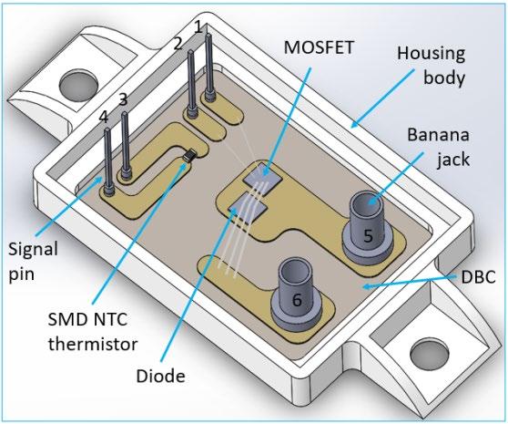
Fig. 2. Internal view of HV custom package used to evaluate and verify device performance
• J. Lynch, N. Yun, and W. Sung, “Design Considerations for High Voltage SiC Power Devices: An Experimental Investigation into Channel Pinching of 10kV SiC Junction Barrier Schottky (JBS) Diodes,” International Symposium on Power Semiconductor Devices and ICs (ISPSD), May 2019, doi: 10.1109/ISPSD.2019.8757593.
• N. Yun, D. Kim, J. Lynch, A. Morgan, W. Sung, M. Kang, A. Agarwal, R. Green, and A. Lelis, "Developing 13-kV 4H-SiC MOSFETs: Significance of Implant Straggle, Channel Design, and MOS Process on Static Performance," in IEEE Transactions on Electron Devices, vol. 67, no. 10, pp. 4346-4353, Oct. 2020, doi: 10.1109/TED.2020.3017150.
• J. Lynch, N. Yun, W. Sung, I. Deckman, D. Rossman, S. Kim, D. Nguyen, J. Seo, D. Haberstat, M. Hinojosa, R. Green, and A. Lelis, “Demonstration of High Voltage (15kV) Split-Gate 4H-SiC MOSFETs,” Wide Bandgap Power Devices & Applications (WiPDA), November 2021, doi: 10.1109/WiPDA49284.2021.9645153
• N. Yun, J. Lynch, A. J. Morgan, S. deBoer, D. Xing, M. Jin, M. Kang, A. Agarwal, R. Stahlbush, R. Green, A. Lelis, and W. Sung,, “14 kV-Rated Monolithic Integration of 4H-SiC MOSFET and JBS Diode (JBSFET) for High-Power Applications,” IEEE Transactions on Electron Devices, under review.
• N. Yun, J. Lynch, S. deBoer, A. J. Morgan, D. Xing, M. Jin, M. Kang, A. Agarwal, R. Green, A. Lelis, and W. Sung,, “Comprehensive Evaluations of High Voltage,14 kV 4H-SiC Power MOSFETs with Various Channel and Cell Designs” IEEE Transactions on Electron Devices, under review.
• Funding for this work is provided by the Army Research Lab (ARL)
• Key Contributors include: NoMIS Power, SiCamore Semi, Naval Research Lab and Ohio State University
Woongje Sung
Scalable, Manufacturable, And Robust Technology for SiC power integrated circuits (SMART SiC Power ICs)
• This project aims to develop Scalable, Manufacturable, And Robust Technology for SiC power integrated circuits (SMART SiC Power ICs). Disruptive designs and processes were being developed to achieve high-voltage (HV) integrated circuits of large scale (>1 cm2) by monolithically integrating the SiC Complementary Metal-OxideSemiconductor (CMOS) and HV (400 – 600 V) lateral power nMOSFETs on 100-150 mm 4H-SiC substrates
• Approach
Highlights
• SMART IC technology cross-section


Publications


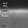


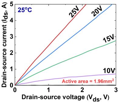

• HV NMOS electrical characteristics
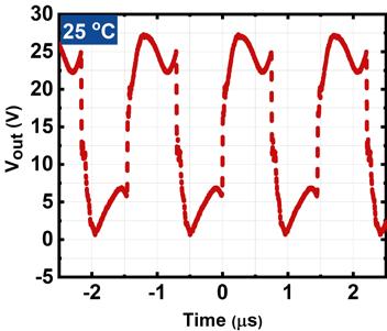
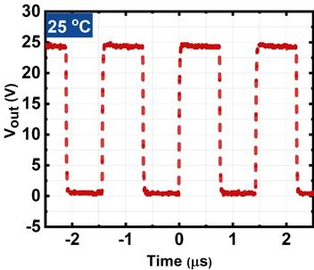
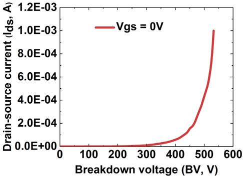
• CMOS IC (ring oscillator) demonstration
• Sundar Babu Isukapati, H. Zhang, T. Liu, E. Ashik, B. Lee, A. Morgan, W. Sung, A. Fayed, and A. Agarwal, “Monolithic Integration of Lateral HV Power MOSFET with LV CMOS for SiC power IC technology,” in 2021 33rd International Symposium on Power Semiconductor Devices and ICs (ISPSD). IEEE, 2021.
• Sundar Babu Isukapati, H. Zhang, T. Liu, E. Ashik, B. Lee, A. Morgan, W. Sung, A. Fayed, and A. Agarwal, “Development of Isolated CMOS and HV MOSFET on an N-epi/P-epi/4H-SiC N+ Substrate for Power IC Applications,” in 8th IEEE Workshop on Wide Bandgap Power Devices and Applications (WiPDA 2021). IEEE, 2021.
• We would like to thank the funding agency ARPA-E and project director Isik Kizilyalli for their valuable inputs. We also thank ADI Hillview facility for the fabrication of the devices. We acknowledge that the channeling implantation used for the junction isolation was conducted by NISSIN ION EQUIPMENT CO., LTD., Kyoto, Japan.
Woongje Sung
CPR (Cost competitive, high Performance, and Rugged) SiC Power Devices for Electric Drive Technologies
• The main objective of this project is to develop 1.2 KV SiC MOSFETs that are superior to their Silicon counterparts (IGBTs) in all aspects, such as cost, performance, and reliability. To accomplish the goal, many different variations in device and process design have been pursue
• SiC MOSFETs with deep P-wells (1.8 μm), formed by using an additional channeling implantation, and short channels (0.3 μm) were proposed that significantly improved the conventional trade-off relationship between Ron,sp and the BV or SCWT
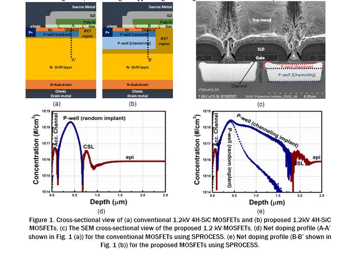
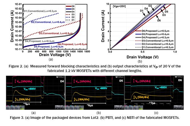
D. Kim, N. yun, S. Y. Jang, A. J. Morgan, and W. Sung, An Inclusive Structural Analysis on the Design of 1.2kV 4H-SiC Planar MOSFETs,” IEEE Journal of the Electron Devices Society, vol. 9, pp. 804–812, 2021, doi: 10.1109/JEDS.2021.3109605
•D. Kim and W. Sung, “Improved Short-Circuit Ruggedness for 1.2kV 4H-SiC MOSFET Using a Deep P-Well Implemented by Channeling Implantation,” IEEE Electron Device Letters, vol. 42, no. 12, pp. 1822–1825, Dec. 2021 doi: 10.1109/LED.2021.3123289
•D. Kim, S. Y. Jang, S. De Boer, A. J. Morgan, and W. Sung, “An Optimal Design for 1.2kV 4H-SiC JBSFET (Junction Barrier Schottky diode integrated MOSFET) with Deep P-well,” IEEE Electron Device Letters, pp. 1–1, 2022, doi: 10.1109/LED.2022.3162156
•D. Kim, N. Yun, S. Y. Jang, A. J. Morgan, and W. Sung, “Channel Design Optimization for 1.2-kV 4H-SiC MOSFET Achieving Inherent Unipolar Diode 3rd Quadrant Operation,” IEEE Journal of the Electron Devices Society, vol. 10, pp. 495–503, 2022, doi: 10.1109/JEDS.2022.3185526
•D. Kim, N. Yun, A. J. Morgan, and W. Sung, “The Effect of Deep JFET and P-Well Implant of 1.2kV 4H-SiC MOSFETs,” IEEE Journal of the Electron Devices Society, vol. 10, pp. 989–995, 2022, doi: 10.1109/JEDS.2022.3218689
•D. Kim, A. J. Morgan, N. Yun, W. Sung, A. Agarwal, and R. Kaplar, “Non-Isothermal Simulations to Optimize SiC MOSFETs for Enhanced Short-Circuit Ruggedness,” in 2020 IEEE International Reliability Physics Symposium (IRPS), Apr. 2020, pp. 1–6 doi: 10.1109/IRPS45951.2020.9128324
•D. Kim, N. Yun, S. DeBoer, A. J. Morgan, S. Y. Jang, W. Sung, J. Fan, S. Yu, M. Kang, and A. K. Agarwal, “A Static, Switching, Short-circuit Characteristics of 1.2 kV 4H-SiC MOSFETs: Comparison between Linear and (Bridged) Hexagonal Topology,” in 2021 IEEE 8th Workshop on Wide Bandgap Power Devices and Applications (WiPDA), Nov. 2021, pp. 9–13 doi: 10.1109/WiPDA49284.2021.9645098
•D. Kim, S. Y. Jang, A. J. Morgan, and W. Sung, “Implementation of a short channel (0.3 μm) for 4H-SiC MOSFETs with deep P-well using ‘channeling’ implantation,” in 2022 IEEE 34th International Symposium on Power Semiconductor Devices and ICs (ISPSD), May 2022, pp. 217–220 doi: 10.1109/ISPSD49238.2022.9813633
•D. Kim, S. DeBoer, S. Y. Jang, A. J. Morgan, and W. Sung, A Comparison of Short-Circuit Failure Mechanisms of 1.2 kV 4H-SiC MOSFETs and JBSFETs,” in 2022 IEEE 9th Workshop on Wide Bandgap Power Devices & Applications (WiPDA), Jan. 2022, pp. 54–57 doi: 10.1109/WiPDA56483.2022.9955302
D. Kim, S. DeBoer, S. A Mancini, S. B. Isukapati, J. Lynch, N. Yun, A. J. Morgan, S. Y. Jang, and W. Sung, A Static, Dynamic, Short-circuit Characteristics of Split-Gate 1.2 kV 4H-SiC MOSFETs,” In 2023 IEEE International Reliability Physics Symposium (IRPS), accepted.
•Funding for this project comes from the Office of Energy Efficiency and Renewable Energy (EERE), U.S. Department of Energy, and the Vehicle Technologies Program Office.
•The authors would like to thank SiCamore Semi, Bend, OR for the fabrication of the devices. The authors acknowledge that the channeling implantations for the proposed devices were conducted by NISSIN ION EQUIPMENT CO.,LTD., Kyoto, Japan.
• This project aims to 1) design and optimize 1.2kV SiC Trench MOSFET cell structure to achieve a low on-resistance, a highly efficient edge termination structure, a reasonable threshold voltage, circuit-oriented switching behaviors, and the avalanche ruggedness, and 2) establish a process baseline to fabricate the proposed MOSFETs. Designs, fabrications, and characterizations of three lots for MOSFETs devices are planned.
• 1.2 kV SiC trench MOSFET cell structures were optimized in terms of Ron,sp, BV, and Eox
• Extensive 2-D device simulations have been conducted under a support of a private company.
• 56 different devices were designed for Lot1.
• The process baseline for 4H-SiC trench MOSFET is being developed at a 6-inch foundry partner company.
• The outcome of this project will allow next generation power devices on SiC, further reducing power loss for many different applications such as EV power inverters, fast chargers, and consumer electronics.

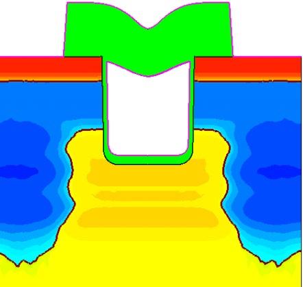

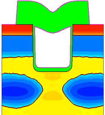

Sung
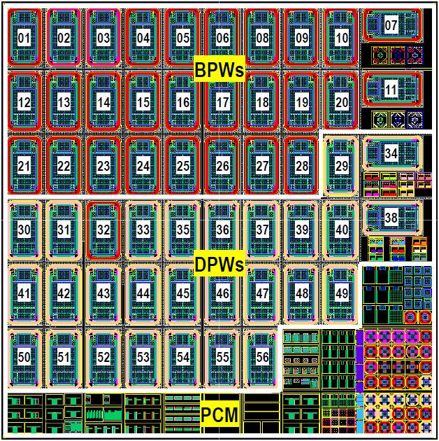
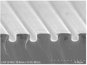
• The sxRNA approach is based on the binding of one RNA molecule to a second RNA molecule in a designed manner This allows us to target the presence of a cellular or disease specific RNA to act as a “Trigger” to change the structure of a “Bait” RNA that has been engineered to turn ON when the two RNAs interact
• This mechanism provides a unique ‘ON/OFF’ switch for the controlled expression of target protein. Unlike other technologies that only turn off gene expression, the switchable gene expression control system offered by the sxRNA platform provides a means to turn ON the gene expression
• By coupling the protein expression with the unique RNA signature of a cell, our sxRNA technology enables the tissue-specific expression of a selected gene product and the ability to control this expression at the level of mRNA rather than DNA.
• sxRNA creates many new possibilities for RNA-based gene therapies, diagnostics, and biomanufacturing as well as other medical applications. For example, sxRNA could be used to express a suicide protein specifically in pancreatic cancer tissue or integrated into a pointof-care test used to screen for exposure to the SARSCOV2 or incorporated into the biomanufacturing pipeline to speed up the process and increase yield
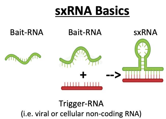
sxRNA Diagnostics
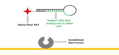
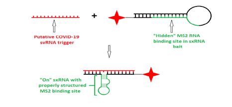
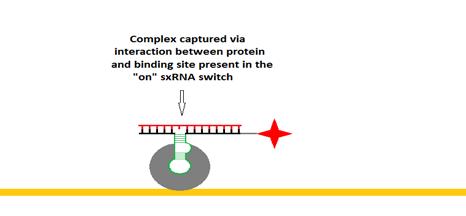
Publications

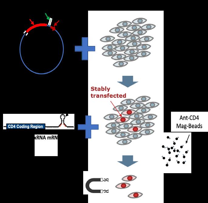
• PTSelect™: A post-transcriptional technology that enables rapid establishment of stable CHO cell lines and surveillance of clonal variation. Muralidharan-Chari V, Wurz Z, Doyle F, Henry M, Diendorfer A, Tenenbaum SA, Borth N, Eveleth E, Sharfstein ST. J Biotechnol. 2021 Jan 10;325:360-371.
• Redox and mTOR-dependent regulation of plasma lamellar calcium influx controls the senescence-associated secretory phenotype. Chandrasekaran A, Lee MY, Zhang X, Hasan S, Desta H, Tenenbaum SA, Melendez. JA.Exp Biol Med (Maywood). 2020 Nov;245(17):1560-1570.
• Surface Enhanced Raman Spectroscopy for Single Molecule Protein Detection. Almehmadi LM, Curley SM, Tokranova NA, Tenenbaum SA, Lednev IK. Sci Rep. 2019 Aug 26;9(1):12356.
• FASTmiR: an RNA-based sensor for in vitro quantification and live-cell localization of small RNAs. Huang K, Doyle F, Wurz ZE, Tenenbaum SA, Hammond RK, Caplan JL, Meyers BC. Nucleic Acids Res. 2017 Aug 21;45(14
• Engineering Structurally Interacting RNA (sxRNA). Doyle F, Lapsia S, Spadaro S, Wurz ZE, Bhaduri-McIntosh S, Tenenbaum SA. Sci Rep. 2017 Mar 28;7:45393. doi: 10.1038/srep45393.
Scott Tenenbaum
• NIH NIGMS R01/S1, SUNY Poly CAT, SUNY Poly Internal Seed Funding stenenbaum@albany.edu
http://sxrna.sunycnse.com/nanobio/tenenbaum/
• Certain trace elemental impurities can cause embrittlement of copper interconnects in semiconductor devices, degrading their performance. Some elements, such as bismuth, segregate to the grain boundaries, so even small amounts are problematic.
• Many other elements have little impact on the fracture toughness. There appears to be little correlation with valence or atom size.
• Density Functional Theory is a tool for understanding the distribution of valence electrons in material systems, and can give insight into physical behaviors as well as help interpret other experimental data.
• In this case, it was found that when impurity atoms have a valence number very difference from the host Cu, an ionic character develops. However, transition metal impurities provide a high density of states at the Fermi level (i.e., empty d-orbitals) allowing for screening of the ionic charges and enabling ductility.
• We conclude that simple metal impurities with low solubility in Cu may give rise to brittleness, with the extent correlating with increased valence.
• In preparation Acknowledgements
• This work is in support of an NSF funded project, in collaboration with Prof. K. Dunn (PI).
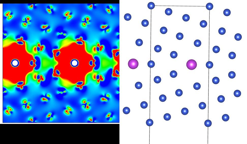
• Redistribution of valence electrons caused by impurity atoms substituting for copper in the grain boundary. Bismuth, with five valence electrons develops a positive charge of 1.3 (indicated in red) while the adjacent GB copper has a slight negative charge (indicated in blue).
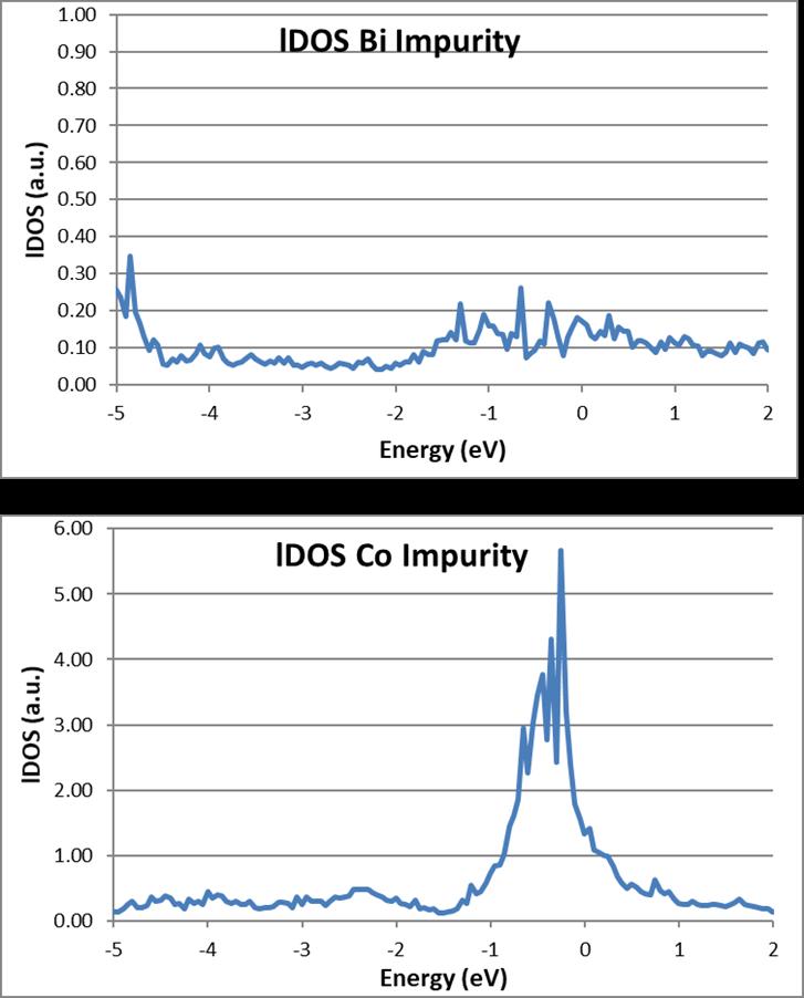
• Local Density of States at the impurity site in the grain boundary. Bi results in a low DOS, correlating with brittleness, whereas the high DOS from Co retains toughness. Publications
Brad Thiel
• The miniaturization of microelectronic devices is typically done by a top -down approach using lithography and plasma etching steps. The current nanometric dimensions make this miniaturization more and more expensive and complex (use of EUV lithography, double and quadruple patterning steps). This can result in edge placement error of a few nm on a 300 mm wafer. A promising solution is to reduce the lithography and etching steps by developing a bottom-up process, where a material is directly and selectively deposited on a surface, which is called area selective deposition (ASD)
• Three different ASD projects are currently being developed at CNSE thanks to the support of the TEL innovation scientist grant and a grant from the Semiconductor Research Collaboration (SRC).
- Study of small inhibitors for ASD by inhibition (TEL grant, Ph.D. work of Anthony Valenti)
- ASD by PECVD on metal organic resist (TEL grant, Ph D work of Rosanna Robert)
- ASD by physisorption on EUV resist (SRC grant, Ph.D. work of Paul Ph.D. of Nicolas Paul Maldonado)
Publications
• M. Bonvalot, C. Vallée, et al. , Area Selective Deposition using alternate deposition and etch super-cycle strategies, Dalton Trans. 51 ( 2022) 442-450
• A. Valenti has developed a specific XPS methodology which permits to characterize the presence of nanoscale inhibitors on the surface of oxides
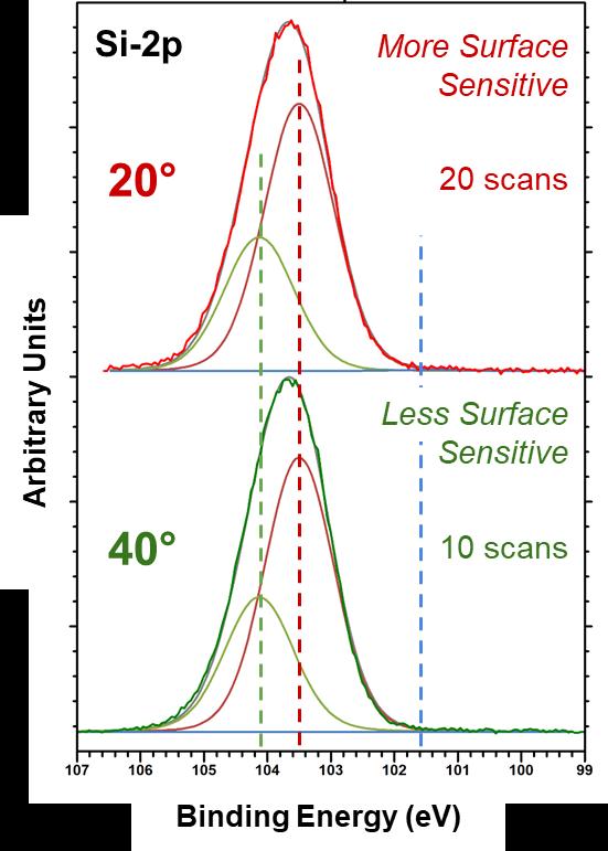
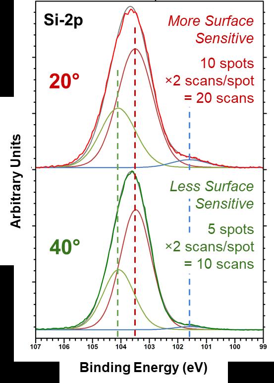
• R . Robert has developed a PECVD process allowing to obtain 6 nm of selectivity between two surfaces. The mechanisms implemented are based on deposition/etching competitions on one surface and radical diffusion/saturation on another
• N.P. Maldonado has built a vacuum chamber for its selective deposition test by physisorption which can be assisted by plasma and/or electron gun. An in-situ ellipsometer has also been mounted on the reactor With this equipment, it has ben demonstrated that some gases used in plasma etching processes can be selectively physisorbed on an EUV resist leading to an ASD process.
This research project is funded by the TEL innovation Scientist grant, CATN2 program, and the SRC
Christophe Vallée, Carl A. Ventrice, Jr, and Greg Denbeaux
cvallee@albany.edu , cventrice@albany.edu , gdenbeaux@albany.edu
• Plasma, the 4th state of matter, is essential for the fabrication of microelectronic devices. It is used either for deposition (PVD, PECVD, PEALD) or for etching (RIE, Plasma ALE ...). When it is used for etching, it must be optimized, and the success of the associated process is described by i) profile control (isotropic vs anisotropic etching), ii) etching rate, iii) selectivity (ability to etch faster a selected material), III) control of induced defects (chemical modification of materials in contact with the plasma, roughness, etch residues).
• In order to produce smaller and smaller 3D patterns with a high aspect ratio, this etching process is constantly being made more complex: plasma pulsing, plasma ALE (Atomic Layer Etching), cryogenic etching...
• This research activity is mainly done in collaboration with the company TEL and the goal is to optimize some plasma etching processes essential to the miniaturization efforts. Optimizing the external parameters (RF power, pulse, pressure, gas selection...) of the reactor requires an excellent understanding of the plasma/surface interactions and the dissociation mechanisms of the precursors in the gas phase. This requires the implementation of in situ diagnostics of the gas phase and/or the thin film being processed on the reactors (OES and ellipsometry for example).
Publications
• In Progress
• During his first year of research on advanced metal etching, I. Otto (Ph.D. student) clearly showed that the chemistry of the walls of a 300 mm etching reactor could strongly modify the etching rates of different materials exposed to the plasma Thus, with an adapted reactor cleaning strategy, an etch selectivity could be achieved between a metal layer and an oxide, which is not possible without this optimization. These results were presented at the AVS conference in 2022 and a paper is currently being submitted
• D. Santos (Ph.D. student) studied the impact of temperature and gas selection for etching low dielectric constant materials in a 300 mm plasma reactor. He showed that by reducing the temperature, for some gases the plasma etching is stopped, and we go into a deposition regime, while for other gases it is accelerated This result can allow to optimize the etching profile of materials with low dielectric constant and limit their modification by the plasma (increase of the dielectric constant). These results have been presented at the AVS 2022 conference and a paper is currently being written for publication
• This research project is funded by the TEL innovation Scientist grant, and the CATN2 program
Christophe Vallee
This research project is a collaborative effort between Menlo Microsystems and my Surface Science research group. Menlo Micro has developed novel RF switches made from microelectromechanical systems (MEMS) These MEMS devices use electrostatically controlled cantilevers to control the propagation of the RF signals. The contact material for the cantilevers is ruthenium It is used as an electrical contact material due to its resistance to oxidation at elevated temperatures. In addition, the most stable stoichiometry of ruthenium oxide under ambient conditions is RuO2, which is an electrically conductive oxide. The goal of this study is to determine the stoichiometry and measured thickness of the surface oxide on Ru formed by typical MEMS fabrication processing techniques. The primary analysis methods used in this study are angle-resolved X-ray photoelectron spectroscopy (AR-XPS) and atomic force microscopy (AFM).
Publications
Air Exposed
Ru-3d
θ = 45°
Δθ = 40°
Ru/SiO2/Si(100)
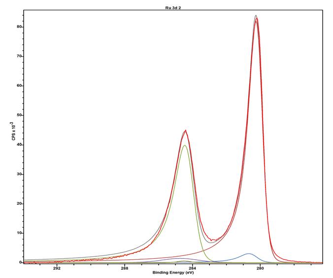
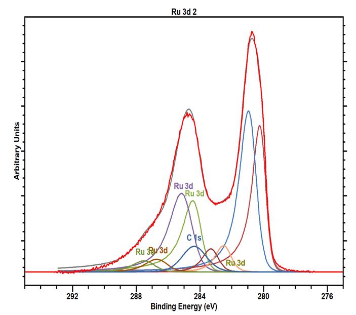
Ru/SiO2/Si(100) Post Anneal
Ru-3d θ = 45°
Δθ = 40°
• Angle-resolved XPS Analysis of the Oxidation of Ru Thin Films, S. Antar, R. Wheeler, A. Valenti, C.A. Ventrice, Jr., M. Strohmayer, J. Brewer, C. Nassar, and C. Keimel, 68th International Symposium of the American Vacuum Society, Pittsburgh, Pennsylvania, November 7, 2022.
Group Members
• Shivan Antar (UG), Anthony Valenti (Grad), and Randall Wheeler (Grad) Menlo Micro Group
• Matthew Strohmayer, Joleyn Brewer , Christopher Nasser, and Christopher Keimel
Acknowledgements
• This research project is funded by the CATN2 program.
Carl A. Ventrice, Jr.
• Salivary gland dysfunction is associated with aging, radiation therapy for head and neck cancers, and the autoimmune disorder, Sjögren’s syndrome. Fibrosis occurs in salivary glands of afflicted individuals, inhibiting tissue regeneration.
• Salivary gland stroma contains tissue-resident mesenchymal stromal cells (MSCs), which have anti-fibrotic potential. To test the hypothesis that exogenous MSCs can revert endogenous fibrotic MSCs to a homeostatic state, reducing fibrosis, we developed fabrication methods to reproducibly produce cryogenic hydrogel nanofiber sponge scaffolds that mimic the ECM topography and biomechanical properties of the salivary gland tissue as well as alginate microfibers. These scaffolds support maintenance of salivary gland tissue-resident MSC phenotype and self-organization of stromal and epithelial cells in vitro.
• This project lays a foundation for bioengineering healthy and fibrotic salivary gland tissues in vitro and delivery of MSCs in vivo to reduce salivary gland fibrosis, leading to salivary gland tissue regeneration.
• Hydrogel nanofiber scaffolds could mimic topographical and viscoelastic properties of soft-tissue ECM, maintain homeostatic phenotype of MSCs, and suppress diseaseassociated fibrotic phenotype.
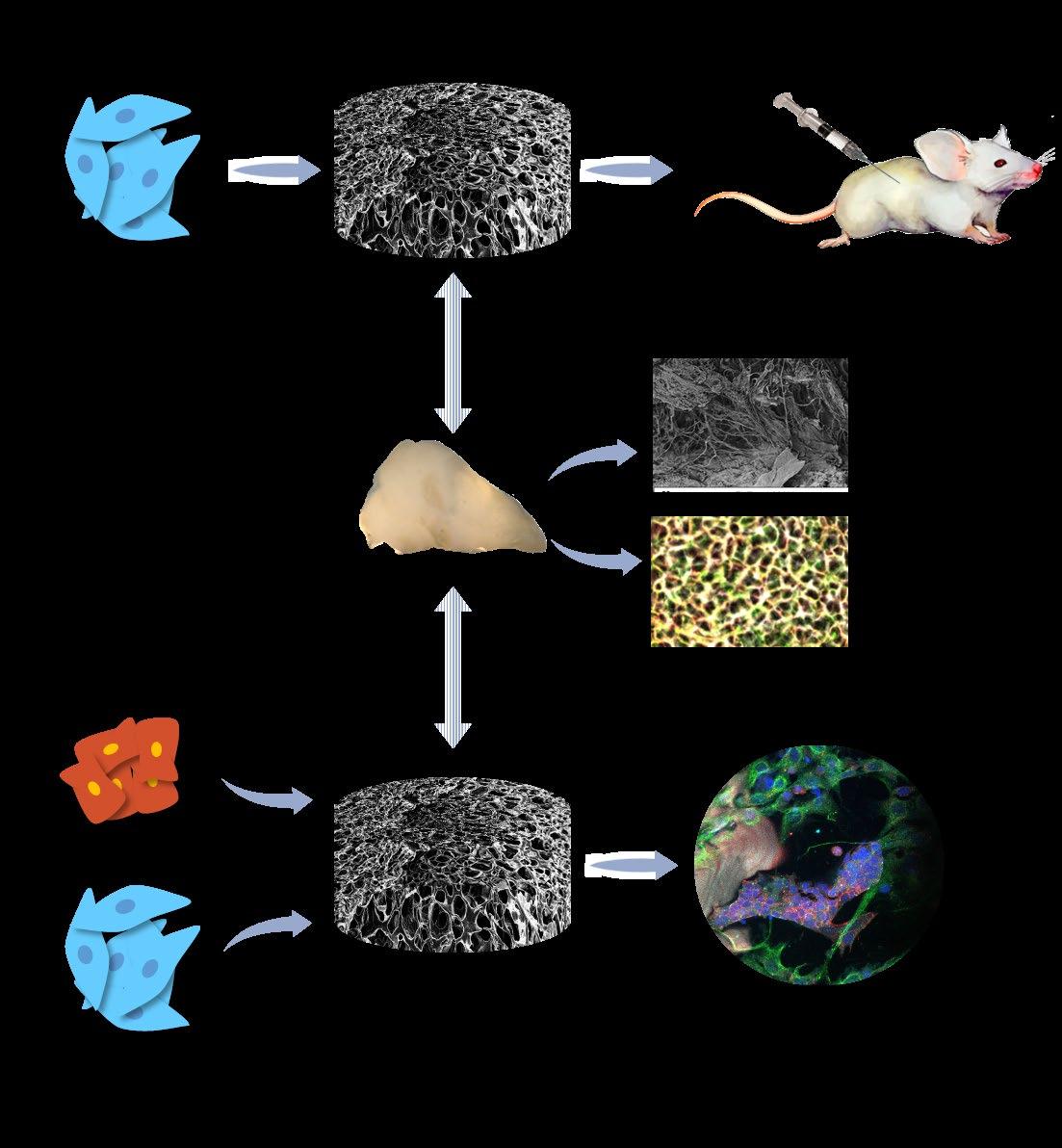
• Xie Y, Kollampally SCR, Jorgensen M, Zhang X. Alginate microfibers as therapeutic delivery scaffolds and tissue mimics. Exp Biol Med. in press. doi: 10.1177/15353702221112905.
• Ramesh P, Moskwa N, Hanchon Z, Koplas A, Nelson DA, Mills KL, Castracane J, Larsen M, Sharfstein ST, Xie Y. Engineering cryoelectrospun elastin-alginate scaffolds to serve as stromal extracellular matrices. Biofabrication 2022 May 17;14(3). doi: 10.1088/1758-5090/ac6b34
• Jorgensen M, Ramesh P, Toro M, Evans E, Moskwa N, Zhang X, Sharfstein ST, Larsen M, Xie Y. Alginate Hydrogel Microtubes for Salivary Gland Cell Organization and Cavitation. Bioengineering. 2022 Jan 15;9(1):38 doi: 10.3390/bioengineering9010038.
• This research is in collaboration with Drs. Mindy Larsen and Susan Sharfstein and funded by NIH National Institute of Dental and Craniofacial Research (NIDCR), grant number R01DE027953 to M.L.
Functional and Integrative Tissue Generation Center (FITGC) aims to promote convergent research, education and workforce training, and technology innovation and translation for widely-accepted adoption of next generation tissue engineering.
• Research on functional cell-biomaterial interactions and multicellular interactions for directed cell regulation based on biomaterial science and cell biology/physiology;
• Development of enabling technologies for engineering cell organization and tissue function employing real-time biosensing to promote longevity and functional outcomes while enabling biomanufacturing in a scalable and reproducible manner;
• Translation of innovation in integration to generate reproducible, scalable, functional cell/tissue/organoid products for biological studies, drug testing, cell therapy and regenerative medicine.
Publications
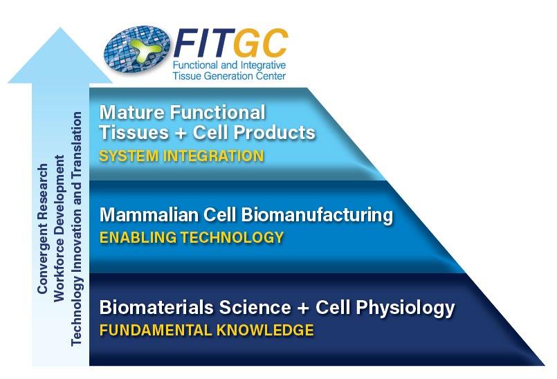
• Bioengineering Ocular Outflow Physiology for High-throughput Drug and Gene Screening
• Nanofiber Scaffolds for Salivary Gland Regeneration
• Hydrogel Microtubes for Organoid Cultures
• Controlled-Release Sutures for Wound Healing and Regenerative Medicine
• T Cell Manufacturing and Novel Bioreactors
• Xie Y, Kollampally SCR, Jorgensen M, Zhang X. Alginate microfibers as therapeutic delivery scaffolds and tissue mimics. Exp Biol Med. in press. doi: 10.1177/15353702221112905.
• Ramesh P, Moskwa N, Hanchon Z, Koplas A, Nelson DA, Mills KL, Castracane J, Larsen M, Sharfstein ST, Xie Y. Engineering cryoelectrospun elastin-alginate scaffolds to serve as stromal extracellular matrices. Biofabrication. 2022;14(3). doi: 10.1088/1758-5090/ac6b34.
• Jorgensen M, Ramesh P, Toro M, Evans E, Moskwa N, Zhang X, Sharfstein ST, Larsen M, Xie Y. Alginate Hydrogel Microtubes for Salivary Gland Cell Organization and Cavitation. Bioengineering. 2022;9(1):38. doi: 10.3390/bioengineering9010038.
• Jorgensen M, Gibbons A, Sui K, Carpenter R, Zhang X, Xie Y. Predictable fabrication of pre-made alginate hydrogel microtubes for stem cell aggregation using needle-in-needle devices. Biofabrication. 2021;13(3). doi: 10.1088/1758-5090/abfd7b.
• Susan Sharfstein, Center Co-director and Xulang Zhang, Center Manager
• NYS CATN2, FuzeHub Manufacturing Grant, SUNY Poly Seed Grant, NIH NIDCR R01DE027953 (Larsen), NIIMBL PC4.1-146 (Sharfstein) & NSF ECCS (PI Sharfstein/co-PIs Cady, Geer, Fahrenkopf & Xie)
Yubing Xie
• As artificial intelligence and big data become ever more present and influential in our lives, there is a need for researchers to confront challenges of digital technology from all walks of life by combining knowledge from both physical and social sciences. In this highly interdisciplinary project, we seek to integrate statistical, computational, and human perspectives of digitization and understand and shape digital transformation of society from its scientific and technological basis to its impact on social and economic inequality.
• How can artificial intelligence and data science learn from physics, transform economic reasoning, financial engineering, and quantitative social research?
• How do current trends of datafication and financialization of digital economy lead to new models of business and new ways of value creation, while reshaping the power imbalance between labor and capital?
• How do advancement of artificial intelligence and automation lead to new ways of working and organizing, impact higher education, and reshape long-term trends of employment precarity and polarization?
Publications
• J. Mao and Y. Xue, Salvaging adulthood at youth work: Dignity, social disrespect, and the micro-politics of recognition in a polarized world, Organization 2022, Vol. 29(6), 1056–1080.
Acknowledgements
• Prof. Jina Mao, Department of Management and Business, Skidmore College