
Surface Studies: Works from On the Surface of Things
Felice Frankel
This selection of images, drawn from Felice Frankel’s landmark book On the Surface of Things, invites us to explore the visual language of science — where form, pattern, and material behavior converge at the boundary between observation and abstraction. Frankel’s photographs are not simply documentation; they are provocations. By transforming scientific processes and phenomena into striking visual compositions, she opens a space where art and science reflect one another. In her lens, surface tension, crystallization, and microscale structures become a vocabulary of texture, rhythm, and light. As one of the leading figures in the field of scientific image-making, Frankel, who is a research scientist in the Department of Chemical Engineering at MIT, challenges us to see beyond data — to recognize the aesthetics of inquiry, and to appreciate the narrative potential of even the smallest material detail.
STUDIO.nano is proud to feature Frankel’s work as a testbed for its digital gallery — a space dedicated to showcasing art, research, and the creative potential of scientific inquiry.
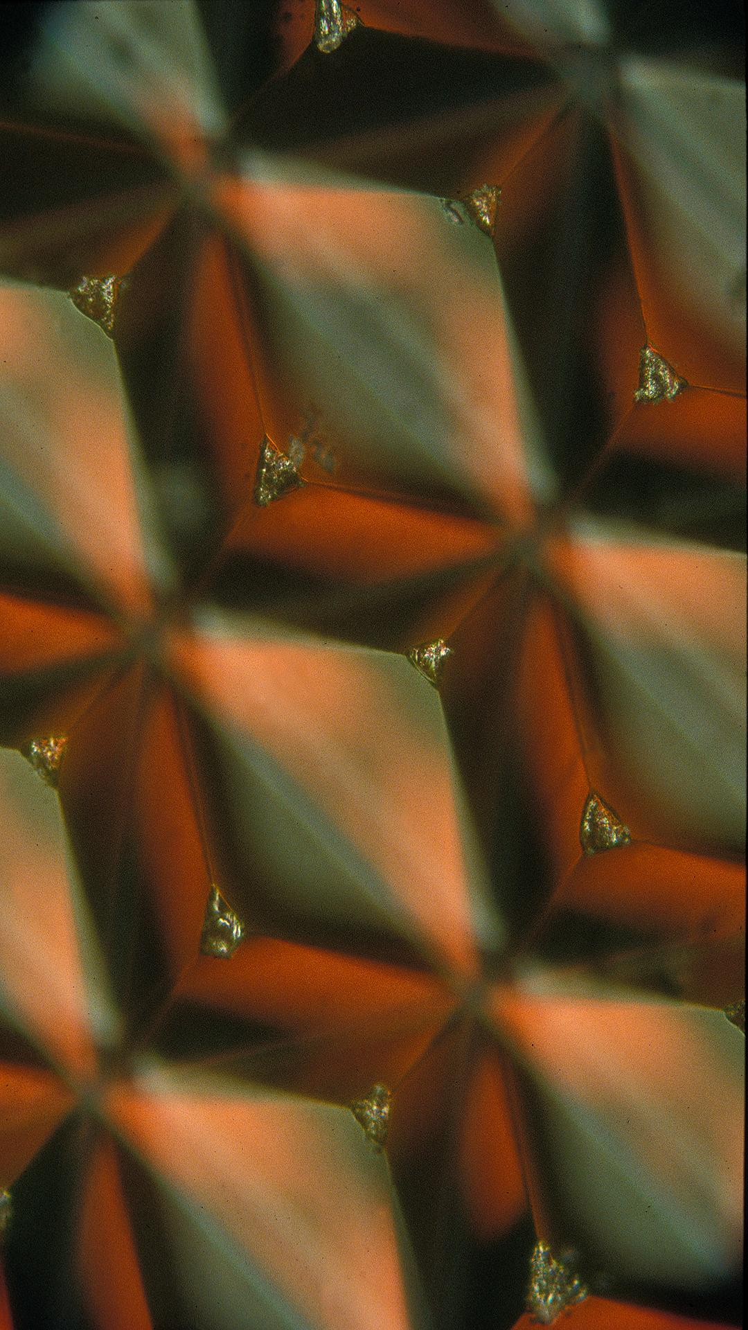
Retroflectors
This array of corner cubes is a 3M product and is part of a broad technology developed by this and other companies based on microreplication. This material is used for optical retroreflectors. Retroreflectors are structures that reflect light back toward its origin. They are widely used in (for example) road signs and bicycle reflectors, where the objective is to reflect light from the headlights of an automobile back to the driver of the automobile. They are also used to enhance the brightness of computer displays by directing more of the light toward the user, to distribute light in illumination systems, and to produce abrasives in which the shapes and orientations of the surfaces used in cutting are precisely controlled.
Gagliardi, J., and T. Buley, “Study of STI polishing defects using 3M fixed abrasive technology,” CMP-MIC Proc., Mar. 9, 2001, pp. 535–38.
Parker, D. H., et al. “Attenuated retroreflectors for electronic distance measurement,” Optical Engineering, 45 (2006), 7.
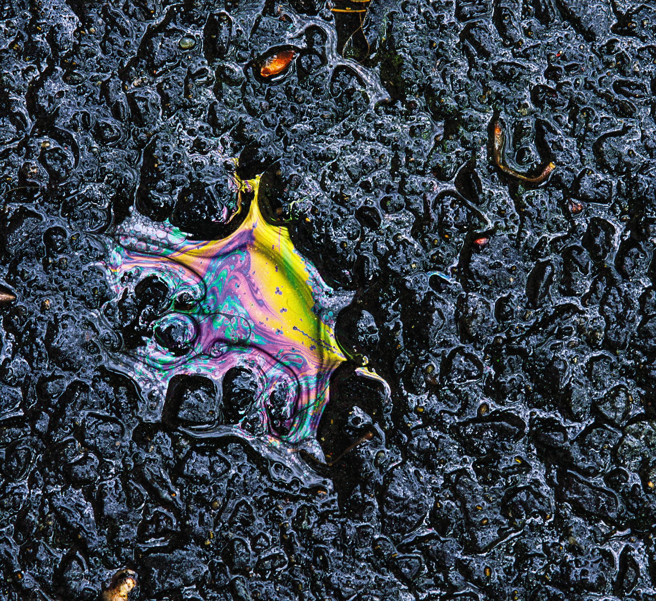
Oil Slick
After hosing down my driveway on a gray Sunday afternoon I searched for one of the more interesting puddles and dropped a bit of oil onto it. I waited half an hour until the diffraction colors became interesting. With the camera and 105mm lens on my tripod I shot perpendicularly to the slick.
Lipson, S. G., H. Lipson, and D. S. Tannhauser, Optical Physics, 3rd ed., Cambridge University Press, Cambridge (1995). Minneart, M.G., Light and Color in the Outdoors, L. Seymor, trans. Springer Verlag, New York (1993).
Moeller, K. D., Optics, University Science Books, Mill Valley, Calif. (1988).
Ramme, G., “Colors on Soap Films—An Interference Phenomenon,” Physics Teacher, 28 (1990), 7, 479–80.
Smith, F. G., and J. H. Thomson, Optics, 2nd ed., John Wiley & Sons, New York (1988).
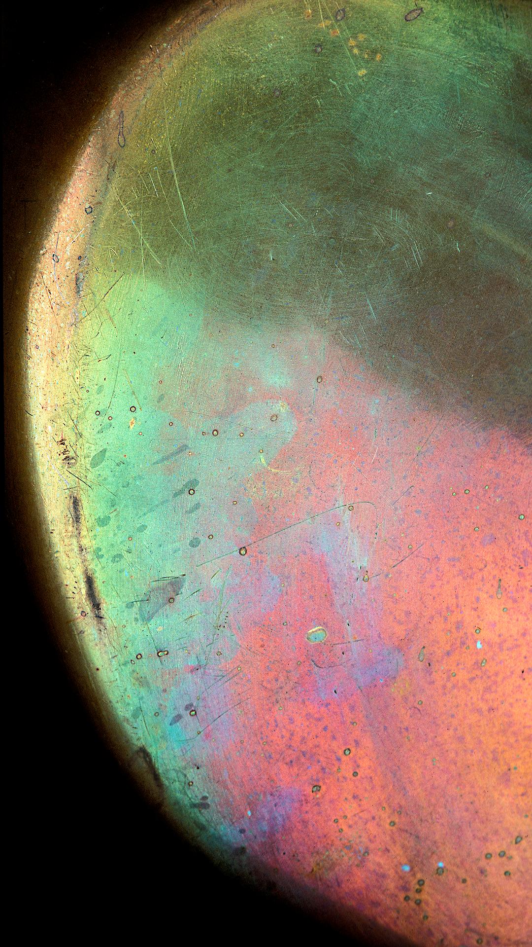
Oxide Layer on a Copper Pan
A friend let me borrow this magnificent au gratin dish. I shot its oxidized underside using daylight with the 105mm lens.
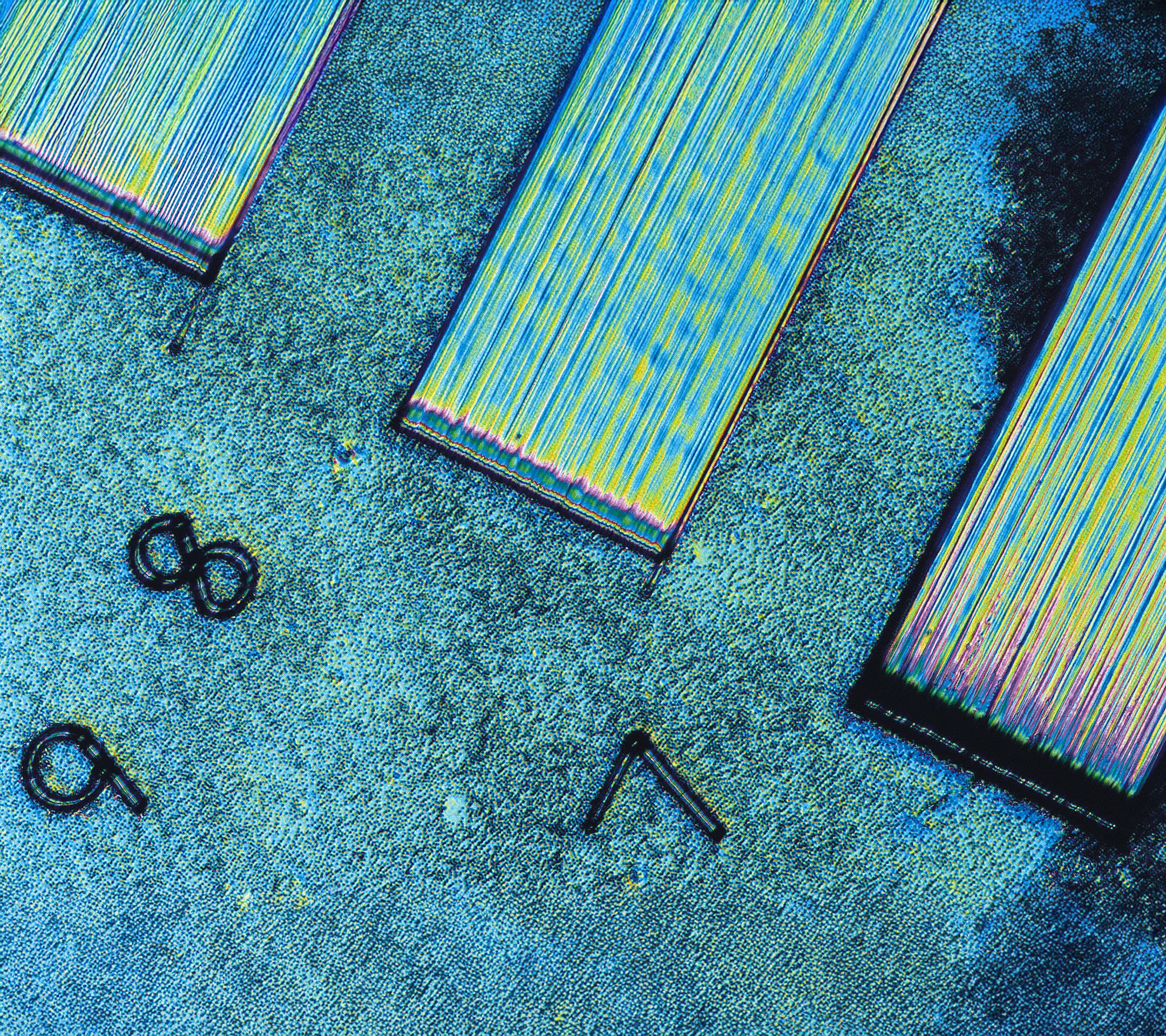
Silicon, Etched by Light
With this technology, three-dimensional structures can be rapidly machined in silicon to micrometer tolerances. This work benefits the emerging field of microelectromechanical systems (MEMS) by extending milling techniques to new size regimes. MEMS merges electronic and mechanical components to produce sensors and actuators such as pressure transducers, valves, and pumps. Current techniques for fabricating these mechanical components rely on lithographic techniques that limit shapes to extrusions of two-dimensional patterns. Laser processing offers a means to produce mechanical components that are inherently more three-dimensional.
Bloomstein, T. M., and D. J. Erlich, "Laser deposition and etching of three-dimensional microstructures," TRANSDUCERS '91: 1991 International Conference on Solid-State Sensors and Actuators, Digest of Technical Papers, 507–11. ———, "Stereo laser micromachining of silicon," Applied Physics Letters, 61 (1992), 708.
Madou, M. J., Fundamentals of Microfabrication: The Science of Miniaturization, 2nd ed., CRC Press, Boca Raton, 2002.

Wing of a Morpho Butterfly
The blue colors of the wing of the morpho butterfly are the result of interference in an elaborately structured set of scales on the wing. The blue is entirely reflected light. The color of the wing (in the absence of the reflections) is a dull grey-brown.
Silver, J., R. Withnall, T. G. Ireland, et al. “Novel nano-structured phosphor materials cast from natural Morpho butterfly scales,” Journal of Modern Optics, 52 (2005), 999–1007. http://webexhibits.org/causesofcolor/15.html
Peterson, I., “Butterfly blue: Packaging a butterfly’s iridescent sheen,” Science News, 148 (1995), 296–97.
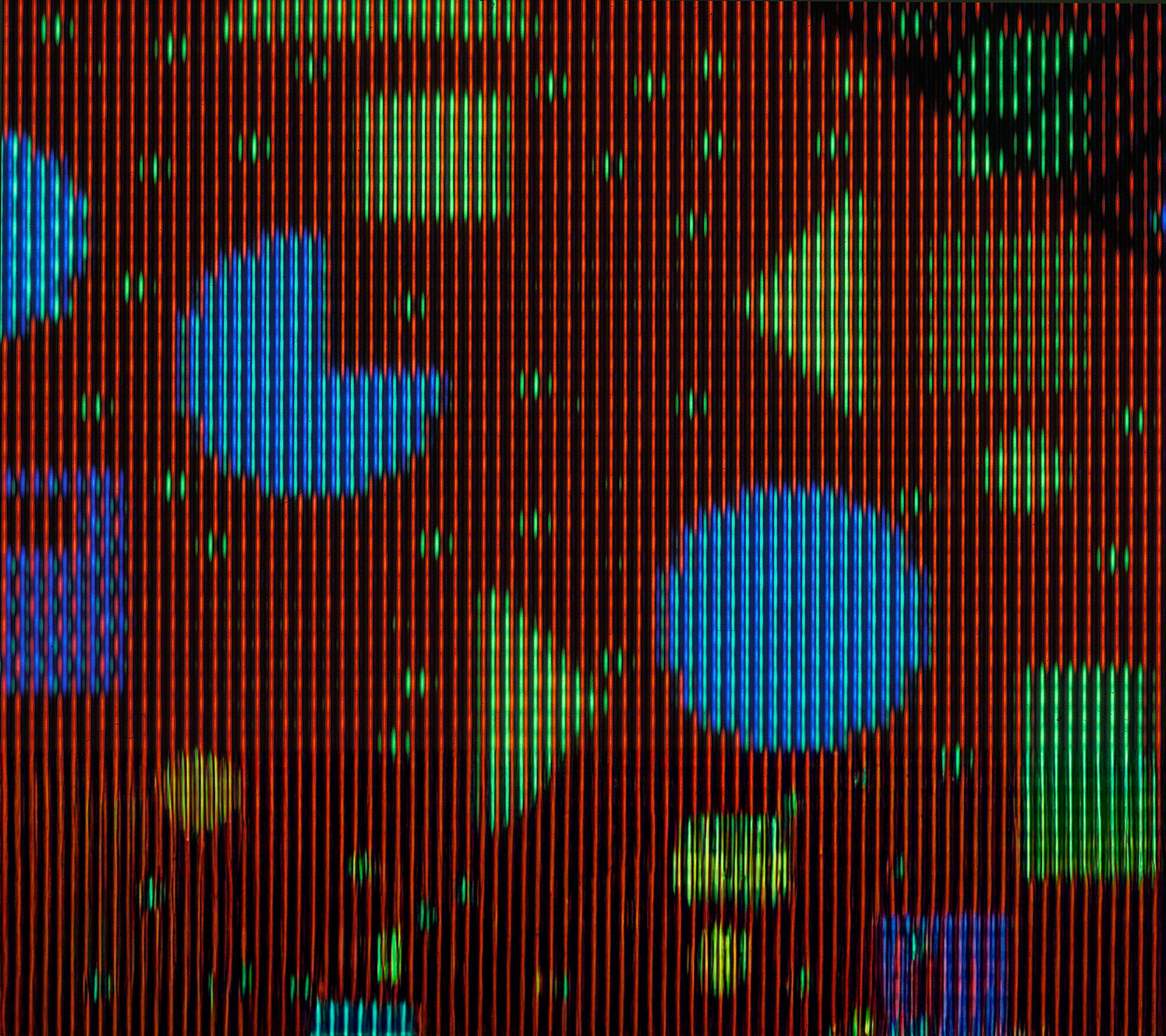
Computer Monitor Screen
I first digitally colored the black and white portion of an image of my coauthor ’s tie (from his home page). I then set up the tripod in front of my computer screen and used a 2x extender on my 105 mm macro and shot with daylight film. I initially tried tungsten but found I preferred daylight film’s color.
DC White, R., How Computers Work, Ziff Davis Press, New York (1993), 115–19. France, M.M. “Reflections on Rippling Water,” American Mathematical Monthly, 100 (1993), 8, 743–48 Lynch, D. K., and W. Livingston, Color and Light in Nature, Cambridge University Press, Cambridge (1995).

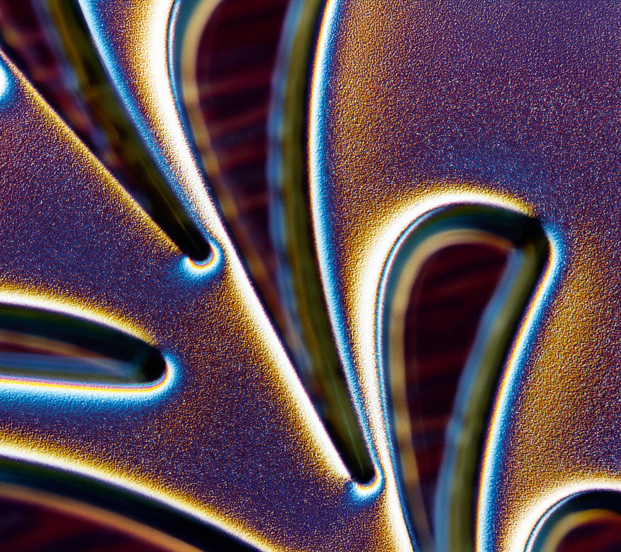
Stamp for Microprinting
I used tungsten lamps to produce the diffraction colors for postdoctoral fellow James Wilbur ’s and Rebecca Jackman’s sample from the Whitesides Lab. A similar image appeared on the cover of Science, August 4, 1995. Ma An elastomeric stamp —made of transparent polydimethylsiloxane (PDMS) is formed by casting the polymer against a master structure that has a pattern of features in bas-relief on its surface. The stamp is “inked” with a compound that forms a self-assembled monolayer onthe surface being patterned: a typical combination is a PDMS stamp, an alkanethiol “ink,” and a flat gold surface. The inked stamp comes into contact with the gold surface; an image complementary to the pattern on the surface of the stamp forms. The resolution of this pattern is remarkable: the roughness of the edges of the pattern is less than 50 nm, even when the process is carried out in the open laboratory. The colors from the front side are those of diffraction of light propagating in air; those from the back side are from diffraction of light propagating in PDMS.
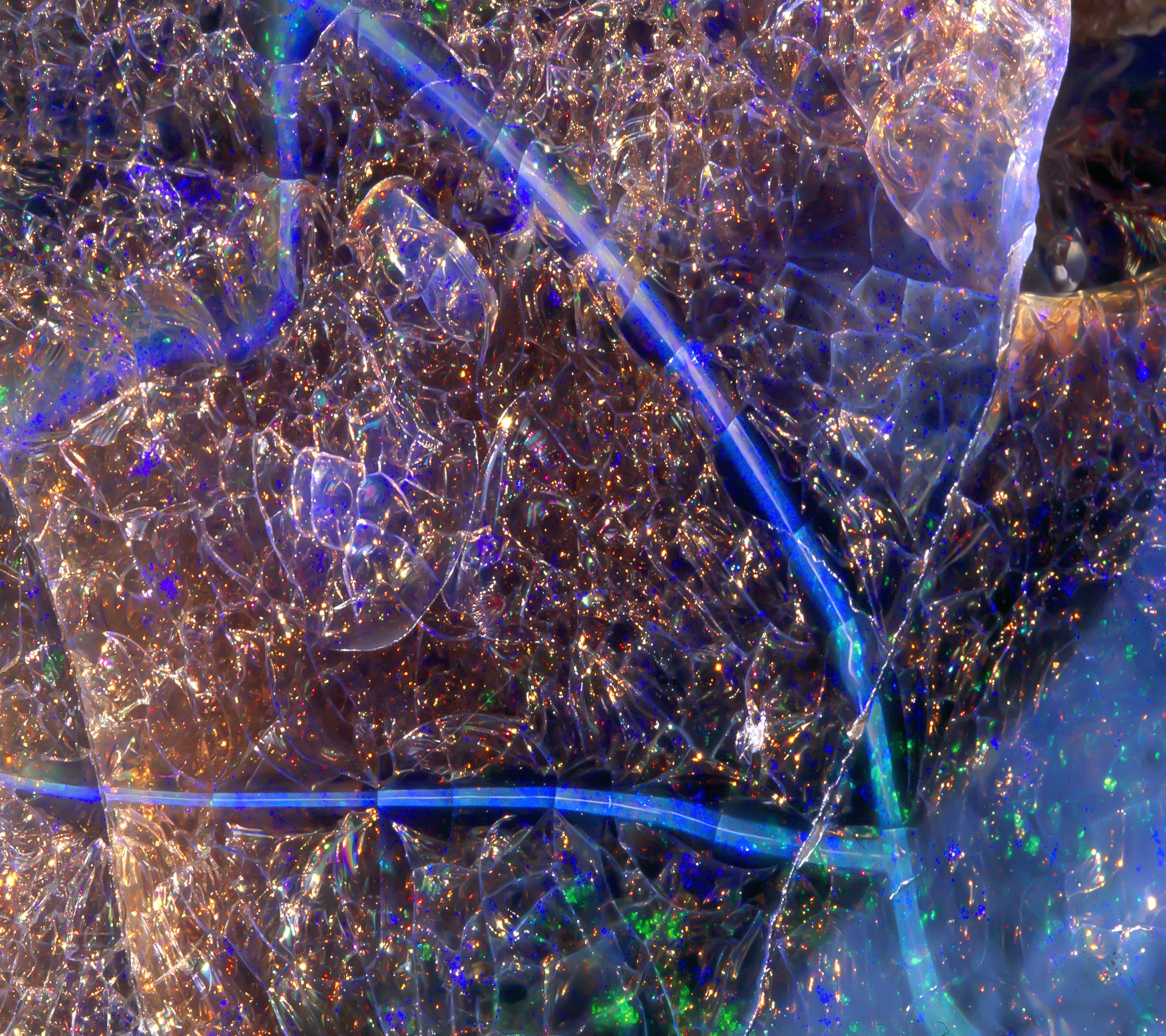
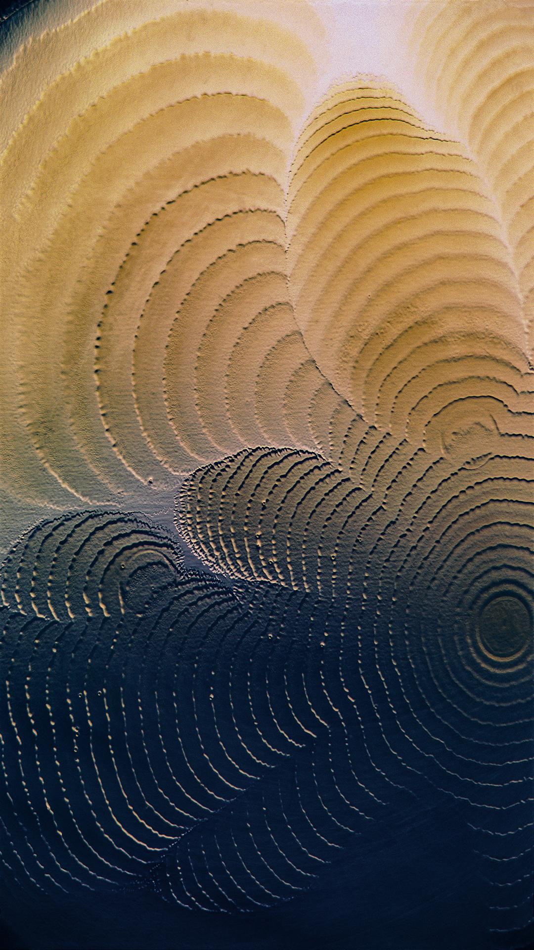
Veins of Opal
William Metropolis, Assistant Curator of the Mineralogical Museum at Harvard University, was kind enough to let me borrow a few large samples of opal. I set this particular specimen under daylight and captured the diffracting light with my 55mm micro lens.
Murray, C. A., and D. G. Grier, “Colloidal Crystals,” American Scientist, 83 (1995) 238–45. Ohara, P. C., et al., “Crystallization of Opals from Polydisperse Nanoparticles,” Physical Review Letters, 75, (1995) 3466–69.
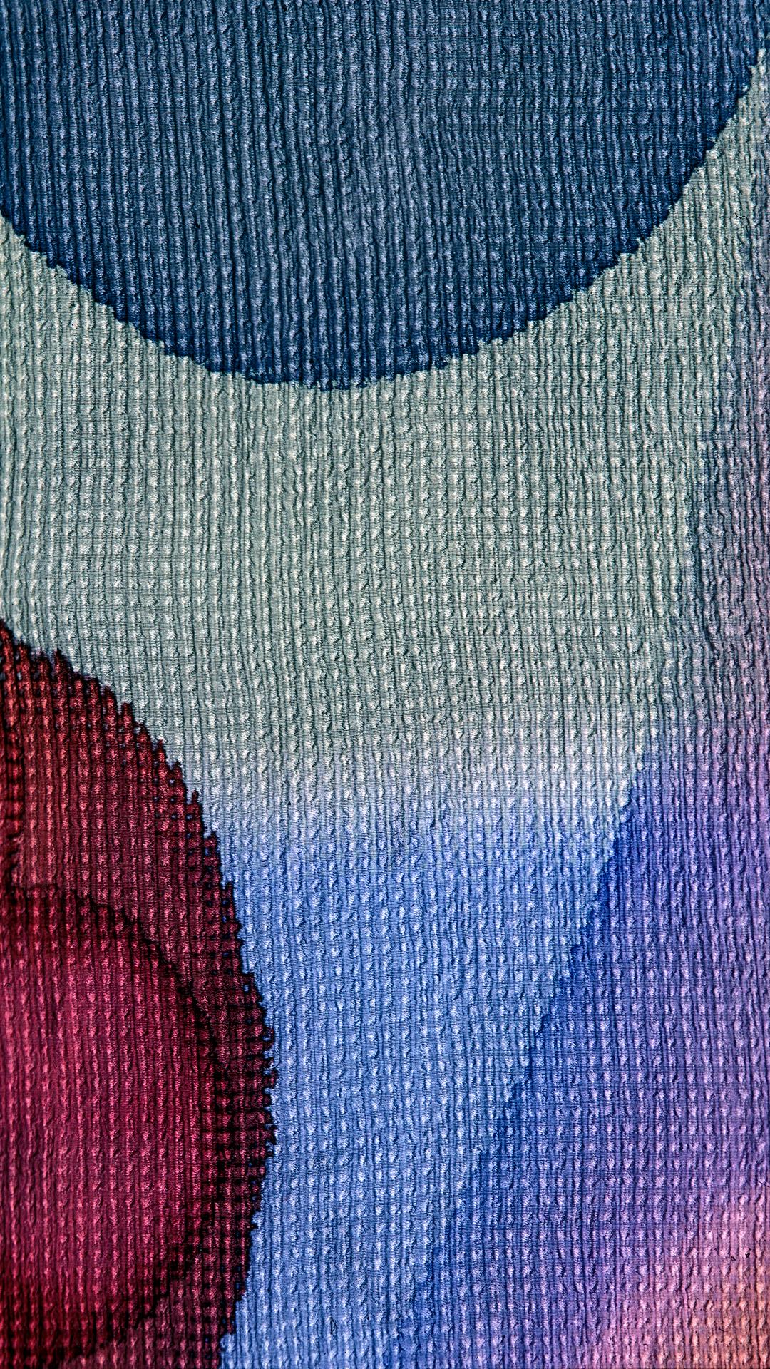
Inks Bleeding on Fabric
This is a detail of my favorite handmade scarves. The artist had placed the inks on the fabric anticipating how far they would bleed. I shot it under diffused daylight with the 55mm lens. Capillary wicking is almost universal on contact of a liquid with a porous solid, so long as the contact angle of the liquid on the solid is less than 90’. The liquid-vapor interfacial free energy may or may not be important in capillary wicking: if the capillaries are completely closed, wicking may result in very little change in liquid-vapor surface area. In wicking of liquid into this porous fabric, there is be a significant increase in the liquidvapor area, and the surface tension of the liquid is important.
Veins of Opal
William Metropolis, Assistant Curator of the Mineralogical Museum at Harvard University, was kind enough to let me borrow a few large samples of opal. I set this particular specimen under daylight and captured the diffracting light with my 55mm micro lens.
Murray, C. A., and D. G. Grier, “Colloidal Crystals,” American Scientist, 83 (1995) 238–45. Ohara, P. C., et al., “Crystallization of Opals from Polydisperse Nanoparticles,” Physical Review Letters, 75, (1995) 3466–69.
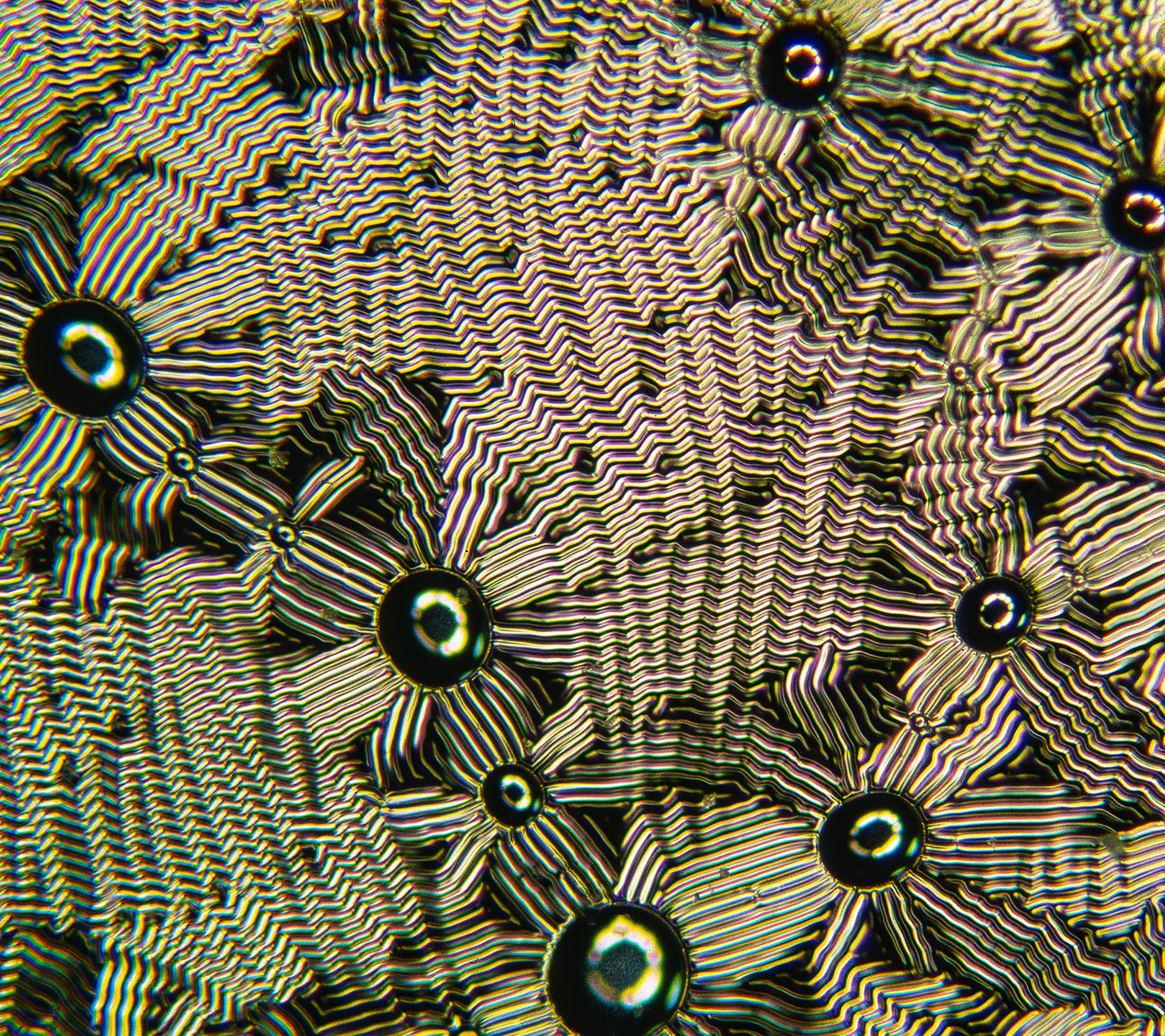
Crystals of Small Particles
I wanted to see how these nano crystals appeared under an optical microscope, Christopher Murray, and Cherie Kagan, then graduate students in Professor Moungi Bawendi’s lab. We’re usually more interested in scanning electron microscopy (SEM). Here I used a blue filter when making the image which suggested that these crystals show luminescence in the yellow part of the spectrum. This image is an optical micrograph of bordered crystals of colloidal particles of CdSe the surface stabilized by a thin, absorbed film of n-alkanethiolate. The colloidal crystals were produced by depositing a drop of suspension of the colloid in a solution on a fused silica slide, and then allowing the solvent to evaporate under reduced pressure.
Murray, C.B., Kagan, C R., and Bawendi, M.G., “Self-Organization of CdSe Nanocrystallites into Three-Dimensional Quantum Dot Superlattices,” Science, 270 (1995), 1335-37
Small Machines
I photographed the blades of a microrotor fabricated by Chunang-Chia Lin from Professors Stephen Senturia and Martin Schmidt ’s lab in the Department of Electrical Engineering and Computer Sciences, MIT. Choosing which plane to keep in focus is always a question in microscopic photography.
Mi, H Gabriel, K. J., “Engineering Microscopic Machines,” Scientific American, 273 (1995), 3, 150–53. Jardin, A. P., et al., eds., Smart Materials Fabrication and Materials for Microelectromechanical Systems, Materials Research Society Proceedings, 276 (1992). Rogers, C. A., “Intelligent Materials,” Scientific American, 273 (1995), 3, 154–61.
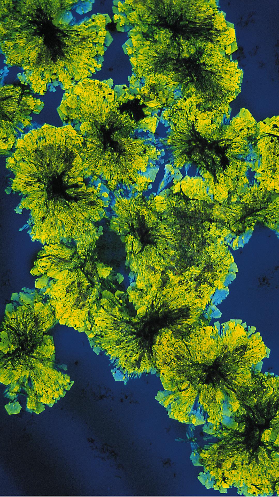
Migrating Bacteria
The light for this shot was unusual: to read the contours I had to combine front lighting with irregular back lighting. Using a magnifying mirror that reflected an irregular background, I placed the petri dish on an angle. Professor James Shapiro in the Department of Biochemistry and Molecular Biology at the University of Chicago was kind enough to bring me samples from Chicago. Ma, C Bacteria are favored organisms for the study of how a stimulus sensed by an organism and converted into a signal inside the cell results in an observable change in behavior. The responses of bacteria to simple chemical signals are reasonably well understood, The behavior of collections of bacteria is much more complicated. The beautiful regularity and complexity of this pattern of Proteus colonies was unexpected. One key to the formation of the visible terraces is the density of growth: when the population of bacteria reaches a certain level, it differentiates a limited subpopulation of swarmer cells that move out and colonize a new region.
Shapiro, J. A., “Bacteria as Multicellular Organisms,” Scientific American, 256 (1988), 82–9. Shapiro, J. A., and D. Trubatch, “Sequential Events in Bacterial Colony Morphogenesis,” Physica, D 49 (1991), 214–23.
Small Machines
I photographed the blades of a microrotor fabricated by Chunang-Chia Lin from Professors Stephen Senturia and Martin Schmidt ’s lab in the Department of Electrical Engineering and Computer Sciences, MIT. Choosing which plane to keep in focus is always a question in microscopic photography.
Mi, H Gabriel, K. J., “Engineering Microscopic Machines,” Scientific American, 273 (1995), 3, 150–53. Jardin, A. P., et al., eds., Smart Materials Fabrication and Materials for Microelectromechanical Systems, Materials Research Society Proceedings, 276 (1992). Rogers, C. A., “Intelligent Materials,” Scientific American, 273 (1995), 3, 154–61.
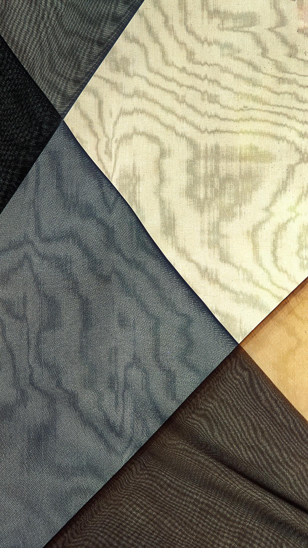
Moiré Pattern
Draping and overlapping a few loosely woven fabrics and attaching them to my window during the day created some interesting moiré patterns.
Kinneging, A. J., “Demonstrating the Optical Principles of Bragg’s Law with Moir. Patterns,” Journal of Chemical Education, 70 (1993), 6, 451–53. Liu, S., “Artistic Effect and Application of Moir. Patterns in Security Holograms,” Applied Optics, 34 (1995), 22, 4700–702.
Mauvoisin, G., F. Bremand, and A. Lagarde, “Three-Dimensional Shape Reconstruction by Phase-Shifting Shadow Moir.,” Applied Optics, 33 (1994), 11, 2163–69.
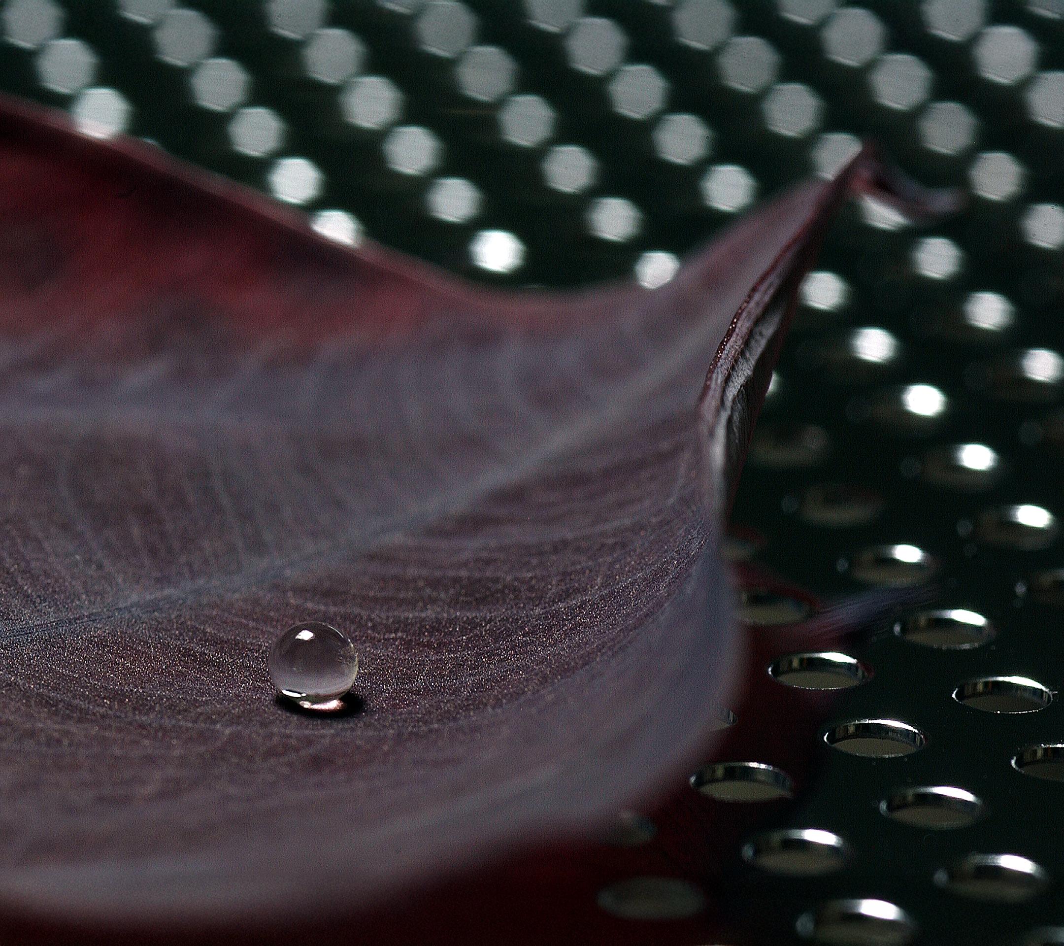
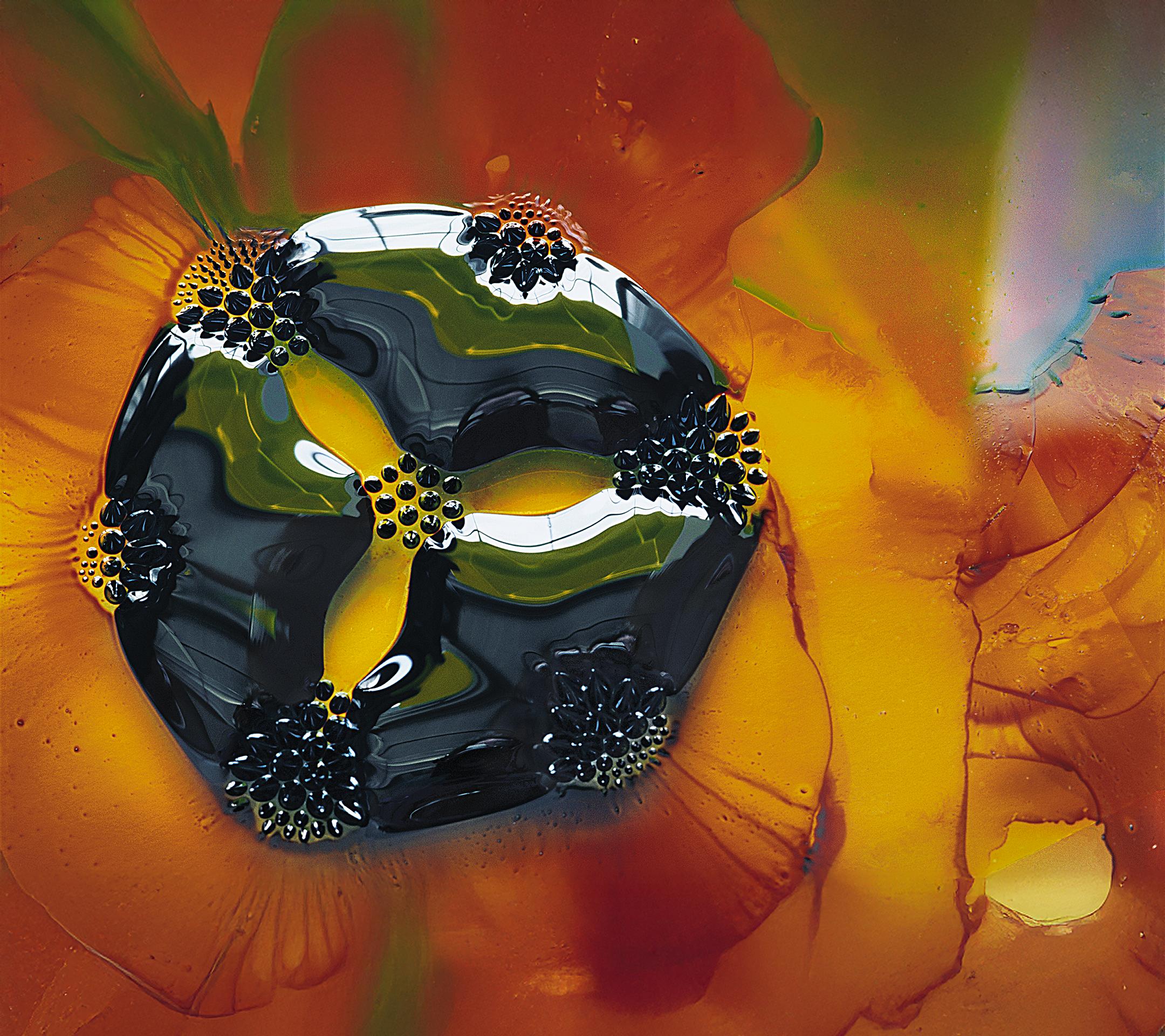
Nonwetting Surfaces
Rob Nicholson from the Botanic Garden at Smith College gave me a number of leaves to play with.
Otten, A., and S. Herminghaus, “How plants keep dry: A physicist ’s point of view,” Langmuir, 20 (2004), 2405–08. Zhai, L., et al., “Stable superhydrophobic coatings from polyelectrolyte multilayers,” Nano Letters, 4 (2004), 1349–53.
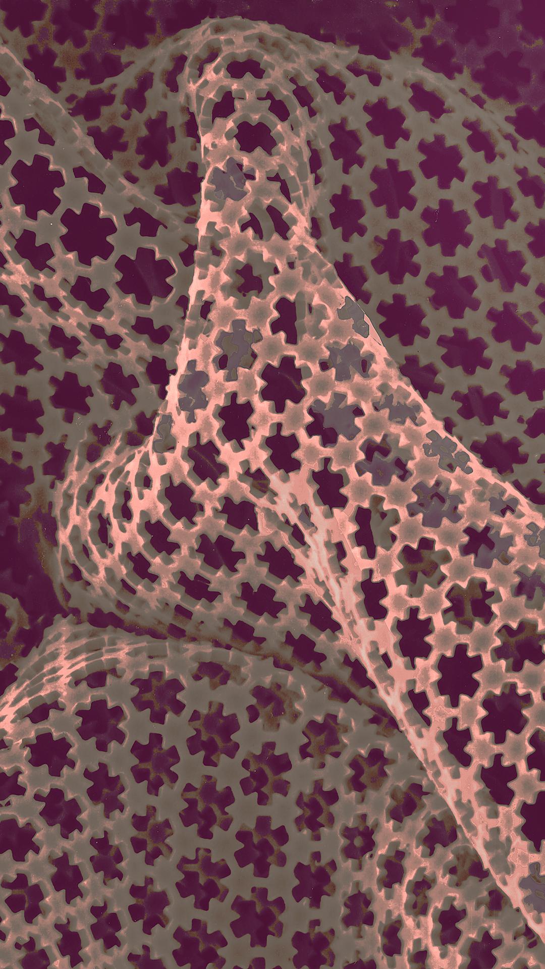
Molded Plastic Microfabric
A transparent polydimethylsiloxane (PDMS) stamp was prepared by casting a liquid prepolymer across a relief structure of photoresist; the pattern was introduced by conventional photolithography. The PDMS stamp, on contact with a flat piece of glass, formed a network of channels with minimum channel diameter of approximately 1 µm. A liquid epoxy prepolymer was brought into contact with this network and filled it by capillarity. Thermal or photochemical crosslinking of the prepolymer (using light transmitted through the PDMS) gave a solid network. Peeling away the PDMS stamp left the network of polymer on the glass, which was then dissolved to release the plastic fabric.
Gates, B. D., et al., “Unconventional nanofabrication,” Annual Review of Materials Research, 34 (2004), 339–72. ———, “New approaches to nanofabrication: Molding, printing, and other techniques,” Chemical Reviews, 105 (2005), 1171–96.
Kim, E., Y. Xia, and G. M. Whitesides, “Polymer microstructures formed by moulding in capillaries,” Nature, 376 (1995), 581–84.