
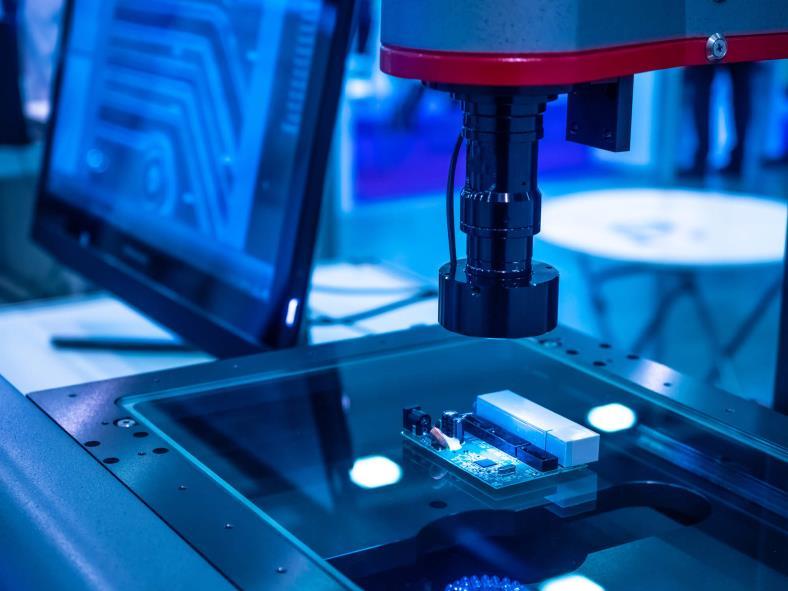
Wafer
Laser Marking Enhancing Semiconductor Manufacturing Efficiency
In the realm of semiconductor manufacturing, precision, and efficiency are paramount. The tiniest imperfections or errors can lead to significant consequences, both in terms of quality and overall performance. One critical aspect of this manufacturing process is wafer laser and marking, a technique that allows for the precise identification and tracking of wafers throughout the production cycle. The significance of wafer laser marking in California's semiconductor industry, its benefits, and how it enhances manufacturing efficiency.
The Importance of Wafer Laser Marking:
• IdentificationandTraceability
In a high-volume semiconductor manufacturing environment, identifying and tracking individual wafers is crucial. Wafer Laser Marking offers a reliable and permanent method to assign unique identifiers to wafers, such as serial numbers, lot codes, or barcodes. These markings are typically etched directly onto the wafer's surface or substrate using laser technology, ensuring durability and longevity throughout the production process.
The ability to trace and identify wafers accurately has numerous benefits. It enables efficient inventory management, and quality control, and prevents mix-ups or errors during assembly and testing stages. By quickly and accurately identifying each wafer, manufacturers can streamline their processes, reduce errors, and ensure consistent product quality.
• Process Optimization and Yield Improvement
Wafer laser marking plays a vital role in optimizing the manufacturing process and improving yield rates. By precisely marking wafers, manufacturers can collect valuable data at each stage of production, allowing them to monitor and analyze the performance of individual wafers, equipment, and processes.
With this data, manufacturers can identify patterns, detect anomalies, and make informed decisions to optimize process parameters. By continuously analyzing the laser markings on
wafers, they can detect any potential issues or variations in real-time, enabling timely adjustments and minimizing defects. This proactive approach to quality control helps improve yield rates, reduce waste, and enhance overall process efficiency.
The Advantages of Laser Marking for Wafers:
• HighPrecisionandDurability
Laser marking technology offers unmatched precision when it comes to marking wafers. The laser beam, controlled by advanced software, can etch intricate patterns, alphanumeric codes, or barcodes onto the wafer's surface with micron-level accuracy. This level of precision ensures that the markings remain legible, even under microscopic inspection, throughout the wafer's lifecycle.
Moreover, laser markings exhibit excellent durability. They are resistant to environmental factors, such as temperature, humidity, or chemical exposure, ensuring that the information remains intact and readable during the manufacturing and testing processes. The longevity of laser markings is particularly crucial for wafers that undergo multiple handling and cleaning steps before final assembly.
• Non-ContactandNon-DestructiveProcess
Wafer laser marking is a non-contact and non-destructive process, making it highly suitable for delicate semiconductor materials. Unlike traditional marking methods that involve physical contact or abrasion, laser marking does not risk damaging the wafer's surface or affecting its electrical properties. This non-destructive nature ensures that the wafer's integrity remains intact, reducing the likelihood of defects or failures during subsequent manufacturing steps.
Furthermore, the non-contact aspect of laser marking eliminates the risk of contamination. Wafer surfaces can be extremely sensitive to foreign particles, which can adversely affect the device's performance. Laser marking avoids introducing any additional contaminants, ensuring the highest level of cleanliness and product quality.
Wafer Laser Marking in California's Semiconductor Industry:
California has long been at the forefront of technological innovation and semiconductor manufacturing. The state is home to numerous high-tech companies, research institutions, and manufacturing facilities that drive advancements in the industry. Wafer laser marking has become an integral part of California's semiconductor manufacturing processes, contributing to the region's success and competitiveness.
• Leading-edgeTechnologyAdoption
The adoption of cutting-edge technologies is a hallmark of California's semiconductor industry. Companies in the region embrace innovative solutions to gain a competitive edge. Wafers laser and marking align perfectly with this mindset by providing a state-of-the-art method for identification and traceability, ensuring that California-based manufacturers maintain their high standards of quality and efficiency.
• StreamlinedManufacturingWorkflows
Efficiency is a key factor in California's semiconductor industry. By incorporating wafer laser marking into their workflows, manufacturers can streamline their operations and minimize the potential for errors or delays. The high precision and durability of laser markings allow for seamless integration with automated systems, reducing the need for manual intervention and optimizing throughput.
Additionally, the data collected from laser-marked wafers can be analyzed using advanced analytics tools to identify bottlenecks, optimize equipment utilization, and predict maintenance requirements. This data-driven approach enables California-based semiconductor manufacturers to achieve higher productivity and shorter time-to-market for their products.
Conclusion:
Wafer laser marking is an indispensable technique in the semiconductor manufacturing industry, and its significance in California cannot be overstated. By providing accurate identification, traceability, and process optimization, Wafer Laser, and marking enhances efficiency, improves yield rates, and ensures consistent product quality. California's semiconductor industry, with its penchant for technological innovation and streamlined workflows, benefits greatly from the precision, durability, and non-contact nature of laser marking. As this sector continues to evolve, wafer lasers will remain a key enabler of progress and success.