
The Silicon Wafer Industry Powering The Digital Revolution
Silicon wafers are the unsung heroes of the digital age. These thin, round slices of silicon serve as the foundation for the fabrication of microchips, the building blocks of modern electronics. From smartphones and laptops to self-driving cars and artificial intelligence, silicon wafers play a crucial role in powering the devices and technologies that shape our world. We will delve into the fascinating world of the Silicon Wafer Industry, exploring its history, manufacturing processes, market trends, and future prospects.
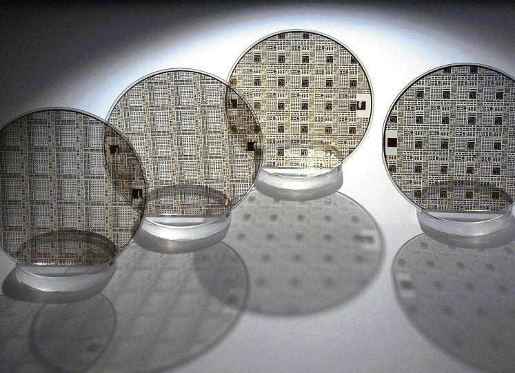
What is a Silicon Wafer?
A silicon wafer is a thin, disc-shaped slice of silicon crystal, usually extracted from a cylindrical ingot through a complex process. These wafers are typically polished to achieve a mirror-like surface and are widely used as a substrate for the fabrication of integrated circuits (ICs) and other electronic components.
Properties and Specifications:
Silicon wafers exhibit unique properties that make them ideal for semiconductor manufacturing. They possess excellent thermal conductivity, high melting point, and exceptional electrical properties, including semiconducting behavior. The size and specifications of silicon wafers have evolved over time, with the most commonly used dimensions today being 200mm (8 inches) and 300mm (12 inches) in diameter. As the industry progresses, there is a growing trend towards larger wafers, enabling higher chip production and lower costs per unit.
Evolution of the Silicon Wafer Industry:
• From Humble Beginnings
The silicon wafer industry traces its roots back to the late 1950s when silicon was first recognized as a promising material for semiconductor manufacturing. The early wafers were small in size,
around 1 inch in diameter, and featured relatively low purity levels. However, with rapid advancements in material science and manufacturing processes, the industry soon witnessed significant growth.
• The Rise of Larger Wafers
As demand for smaller, faster, and more powerful electronic devices increased, the industry shifted towards larger silicon wafers. This transition allowed manufacturers to achieve economies of scale, leading to improved productivity and cost efficiency. In the late 1990s, the 200mm wafers became the industry standard, and by the mid-2000s, the larger 300mm wafers gained prominence. These larger wafers offered several advantages, including increased chip yield per wafer, reduced fabrication costs, and enhanced manufacturing throughput.
Manufacturing Process of Silicon Wafers:
• Crystal Growth
The production of silicon wafers begins with the growth of a high-purity silicon crystal. This process involves heating a silicon feedstock to a molten state and slowly pulling a seed crystal from the melt, allowing it to solidify in a cylindrical shape. This technique, known as the Czochralski method, ensures the formation of a single crystal with a controlled crystallographic orientation.
• Ingot Slicing and Grinding
Once the silicon crystal has solidified, it is cut into thin wafers using a process called ingot slicing. A specialized machine called a diamond wire saw is used to make precise cuts, resulting in the formation of wafer slices with uniform thickness. After slicing, the wafers undergo a grinding process to remove any rough edges and imperfections.
• Surface Polishing and Cleaning
To achieve the desired mirror-like surface finish, the wafers undergo a rigorous polishing process. This involves using a series of abrasive materials and chemical mechanical polishing (CMP) techniques to remove any remaining irregularities. Following polishing, the wafers are thoroughly cleaned to remove any contaminants and particles that could negatively impact the subsequent fabrication steps.
Market Trends and Outlook:
• Increasing Demand for Advanced Electronics
With the proliferation of smart devices, the Internet of Things (IoT), and emerging technologies like 5G and artificial intelligence, the demand for advanced electronics continues to surge. These trends are expected to fuel the growth of the silicon wafer industry, as microchips become smaller, more powerful, and increasingly integrated into various applications, including autonomous vehicles, medical devices, and renewable energy systems.
• Technological Innovations
To meet the demands of next-generation electronic devices, manufacturers are investing in research and development to push the boundaries of silicon wafer technology. Innovations such as three-dimensional (3D) chip stacking, extreme ultraviolet (EUV) lithography, and novel materials are being explored to enhance chip performance and increase transistor density. These advancements are crucial for overcoming the limitations imposed by Moore's Law and enabling the continued progress of the semiconductor industry.
• Regional Landscape
The silicon wafer industry is a global enterprise, with several key players spread across different regions. Asia, particularly Taiwan, South Korea, and Japan has emerged as a dominant force in Silicon Wafer production. These countries boast advanced fabrication facilities, technological expertise, and a robust supply chain, making them vital hubs for semiconductor manufacturing. However, other regions such as the United States and Europe also contribute significantly to the industry's growth and innovation.
Conclusion:
The silicon wafer industry plays a pivotal role in enabling the digital revolution that we are witnessing today. As electronic devices become more powerful, compact, and interconnected, the demand for advanced semiconductor technology continues to soar. Through constant innovation and the adoption of larger wafers, the industry has been able to meet these evolving demands and drive the progress of the electronics industry. Looking ahead, the silicon wafer industry is poised for further growth, as emerging technologies and applications create new opportunities and challenges that will shape the future of our interconnected world.