
The Challenge:
Characterise Copper Interconnect lines (CI) grain boundaries and texture at 1 nm scale
The Solution:
ASTAR technique couple with precession electron diffraction

Unfortunately, CIs that reach lateral sizes of less than 100 nm, with Cu grains smaller than 50 nm, cannot be characterised by conventional techniques like EBSD and XRD, because they do not have enough spatial resolution.
The scaling required to reach faster chip performances in electronic devices has pushed the dimensions of copper interconnect (CI) lines to the nanometer domain. This constant downscaling of CIs implies a change in their microstructure. A change in the grain boundary type distribution and local texture will strongly influence the resistivity and the mechanical reliability of downscaled CIs. A different texture can imply different mechanical properties and a different local distribution of stresses. It is, therefore, necessary to map the textureevolutionwiththesizeofCIs. For reliable texture quantification, it is important to acquire extensive and reliable data sets to have statistically meaningful results and at the same time have a high spatial resolution ASTAR with a parallel nano-sized beam, coupled with a small precession angle, has the appropriate spatial resolution (1 nm) and the reliable pattern indexing which reduces the 180° ambiguities by sampling reflections from higher order zones(HOLZ)
Faster chip performances in electronic devices push CI in nanometer scale
In addition, ASTAR is able to acquire data and index patterns rapidly, which makes it possible to acquire statistically relevant information ASTAR orientation maps reveal the evolution of texture as theCIarescaledfromCIsfrom1.8µmto 70nm
Experimental Data:
TEM Type: JEOL 2010 F
Map resolution: 1 nm
Crystal Structure:
CU: Cubic, Fm3m a=3.610 Å
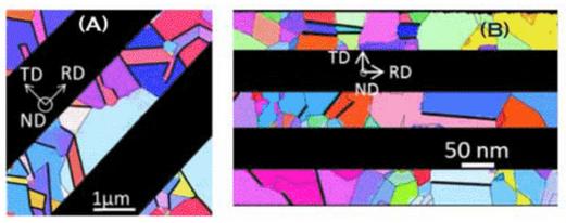
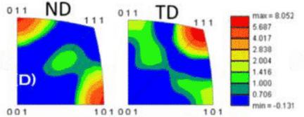
Fig. 1) ASTAR orientation maps of CIs along with texture plots.
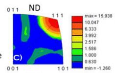
(A) shows the map from 1.8 wide line. (C) plot shows the distribution of crystal directions normal to the trench, Similar plots for the 70 nm wide lines are shown in (b) and (d) figures. Note the change in texture between the two line widths.
InlargeCIstheCugrainshaveastrong <111> fibre texture normal to the trenches(Fig 1)
In the smallest CIs, a <110> texture is observed, normal to the trench while {111} planes are now parallel to the trench sidewalls (Fig 1) The microstructure also changes from a bamboo-like structure in large CIs into a polygranular structure in small CIs, where a polygranular microstructure is a microstructure in which there are continuous grain boundary paths alongthelengthoftheinterconnect.
In the 70 nm CIs grain size is not uniform and clusters of small grains are formed at the bottom of the trenches. Such clusters of small grains adverselyaffectthereliabilityofCIs.


2) Fraction of twin boundaries as a function of line widths. Note the decreasing twin boundary fraction as the line width decreases. Approximately 8000 boundaries extracted from orientation maps was used for this purpose.
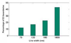
In addition, a decrease in the fraction of coherent twin boundaries was observed withdecreasinglinewidths(Fig 2)
Twin boundaries play an important role in the resistivity performance of CIs. These results are crucial to optimise the process of CI fabrication and to understand how to improve their mechanicalandelectricalproperties.





ASTAR –SEMICONDUCTORS
Ganesh, K J , et al “Automated Local Texture and Stress Analysis in Cu Interconnects Using D- STEM and Precession Microscopy.” Microscopy and Microanalysis, vol 16,no 2,2010,doi:10 1017/S14319276 10061933
STRAIN –SEMICONDUCTORS
A Bashir et al “Strain analysis of a Ge micro disk using precession electron diffraction” J of Applied Physics 2020 DOI: 10 1063/1 5113761
A D Darbal et al “Automated High Precision Strain Measurement Using Nanobeam Diffraction Coupled with Precession” Microscopy & Microanalysis 2013 doi: 10 1017/S1431927613005503
A D Darbal et al “Applications of Automated High Resolution Strain Mapping in TEM on the Study of Strain Distribution in MOSFETs” Microsc Microanal 20 (Suppl 3), 2014 doi:10 1017/S1431927614007053
M.Reisinger et al “Cross-sectional stress distribution in AlxGa1-xN heterostructure on Si(111) substrate characterized by ion beam layer removal method and precession electron diffraction” Materials and Design 106 (2016) 476–481
