

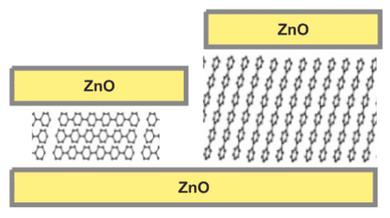
between ZnO substrate - sexipephenyl (6P) - ZnO deposited layer at nm scale
The Solution: ASTAR technique couple with precession electron diffraction
Nanocrystalline ZnO is provided in an inorganic/organic system of ZnO deposited on sexiphenyl (6P).
Initially, 6P was deposited on aplane ZnO substrate at room temperature forming mesoscopic 1-dimensional islands of 6P. In a second step, the islands were capped with ZnO via molecular beamepitaxyat373K.
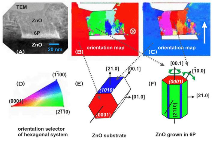
Information on the nanostructure of ZnOgrownatop6Pwasprovidedby high-resolution TEM. Imaging was performed along the [001] direction of the ZnO exhibits a perfect crystal structurewhendirectlygrownonthe substrate. This was confirmed by Fourier transformation (FT) which alsoconfirmedthatZnOgrownatop 6Pundergoesanimperfectgrowth.
Identification of the orientation of thenanocrystalsandindexingofthe lattice planes only based on FT is rather ambiguous and must be handledwithcare.
For this reason, ASTAR was used to uncoveranyspecificsoftheovergrowth regimeofZnOon6Patnmscale.
Optical properties of hybrid systems depend on the nm level structural properties
Flexibleorganic semiconductors

WithASTARscanningtheelectronbeam in nanobeam diffraction mode (probe diameter 1 nm) across an area of 100 nm in width and 80 nm in height providestheorientationmapsdepicted below. The maps were derived by comparing the diffraction pattern recorded at each position with a set of about 1000 calculated diffraction patterns of hexagonal ZnO Focussing on ZnO atop 6P, columnar grains are identified that extend even up to the surface as signified by green and red areas
From the ASTAR orientation map it is evident that the [00.1] wurzite axis is well-aligned along the vertical growth direction indicating a strong texture. Electrostatic forces originating from the 6P molecules have to be considered as the origin of this texture In addition, a significant lateral texture within the (0001) plane cannot be excluded, as it cannotbedistinguishedwhichofthesix prismatic facets contribute to the diffractionpattern
Experimental Data:
TEM Type: JEOL 2200 FS
Map resolution: 1 nm
Scanned area: 100 x 80 nm
Crystal Structure:
ZnO: Hexagonal, P6₃/mmc
a= 3.22 Å
c = 5 20 Å


Research on ZnO is of immediate practical importance as this semiconductor has several favourable properties, including good transparency, high electron mobility, wide bandgap, and strong roomtemperature luminescence These properties are used in emerging applications for transparent electrodes in liquid crystal displays, in energysavingorheat-protectingwindows,and in electronics as thin-film transistors andlight-emittingdiodes(LEDs).
Fig. 1) Crystallographic orientation mapping of ZnO as revealed by scanning nanobeam diffraction (SNBD):
a) TEM image of the region analysed by SNBD b) and c)
crystallographic orientation maps of ZnO The white arrow markers represent the lattice planes colour coded by the orientation triangle of d).
e) alignment of a representative ZnO unit of both, ZnO substrate and low temperature grown homoepitaxial ZnO, f) alignment of a representative ZnO unit for the textured growth atop sexiphenyl


ASTAR –SEMICONDUCTORS
Ganesh, K J , et al “Automated Local Texture and Stress Analysis in Cu Interconnects Using D- STEM and Precession Microscopy.” Microscopy and Microanalysis, vol 16,no 2,2010,doi:10 1017/S14319276 10061933
STRAIN –SEMICONDUCTORS
A Bashir et al “Strain analysis of a Ge micro disk using precession electron diffraction” J of Applied Physics 2020 DOI: 10 1063/1 5113761
A D Darbal et al “Automated High Precision Strain Measurement Using Nanobeam Diffraction Coupled with Precession” Microscopy & Microanalysis 2013 doi: 10 1017/S1431927613005503
A D Darbal et al “Applications of Automated High Resolution Strain Mapping in TEM on the Study of Strain Distribution in MOSFETs” Microsc Microanal 20 (Suppl 3), 2014 doi:10 1017/S1431927614007053
M.Reisinger et al “Cross-sectional stress distribution in AlxGa1-xN heterostructure on Si(111) substrate characterized by ion beam layer removal method and precession electron diffraction” Materials and Design 106 (2016) 476–481