FUSION AX
Machine Vision
Heating and Electrical Characterization System for TEM




What is Fusion AX?
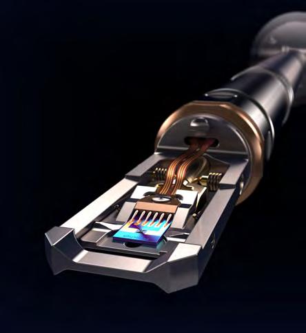
Fusion AX is a revolutionary solution for in situ TEM analysis for materials science, nanoelectronics, and semiconductor devices to drive the development of more robust, cost effective, and efficient materials
What sets Fusion AX apart?
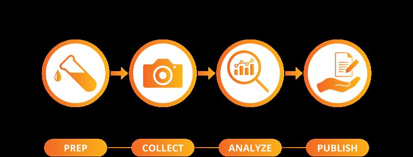
A complete solution from sample preparation to reporting results, Fusion AX will push performance, productivity, and discovery to exponentially high levels for your lab.
The incorporation of first-of-its-kind machine vision software technology, instantly elevates the experience level and skill of the microscopist, enables capture of high resolution and high value data without multiple iterations, and streamlines processing and reporting utilizing only one software.
→ Perform heating, electrical, or electrothermal experiments
→ Friction-free probe design for stable delivery of stimuli
→ Low-profile holder for fast EDS mapping
→ Sample supports with minimal electrical leakage and parasitics
→ Multiple electrical lead layouts to support flexibility in sample preparation
→ Holey carbon support option for heating experiments, maximizing resolution
→ Individually calibrated for temperature accuracy
→ Direct contact between sample and heater during electrothermal experiments
→ Automated drift and focus correction
→ Real-time dose monitoring across the sample
→ Metadata indexing
→ Offline analysis software
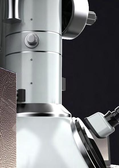

→ A complete suite of products in one holder. Integrated heating, electrical and electrothermal capabilities transform your microscope into a real time laboratory
→ AXON Sychronicity allows you to focus on on the sample and not the TEM controls
→ Confidently, precisely, and repeatably reach high temperatures to study material changes using a unique, inert ceramic heater
→ A unique silicon substrate on the sample supports ensures low electrical leakage and parasitics, enabling accurate electrical characterization of nanoscale samples
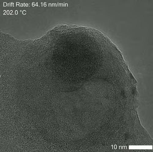
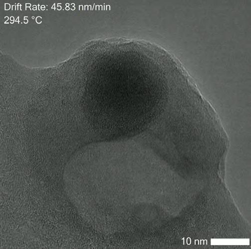
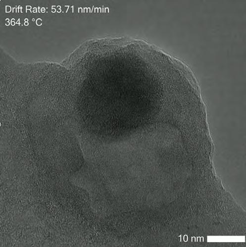
TEM snapshots of gold on iron oxide nanoparticle. The Fusion AX machine vision drift control tracks the sample, centering it perfectly in the field of view during a temperature ramp.
Generate relevant in situ TEM results that complement bulk scale results, opening a direct portal to understanding the causes of material changes in their native environment

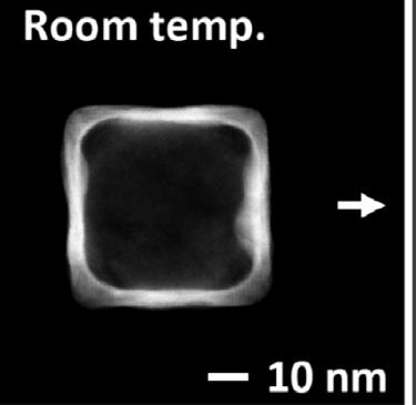

Thermal stability of Ag−Au nanocages

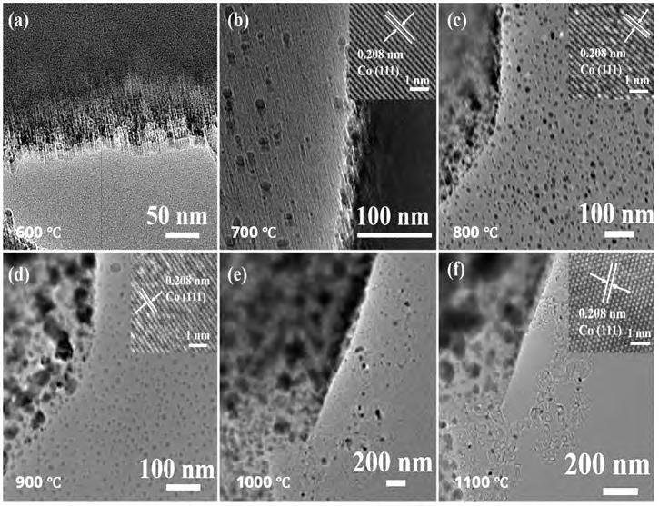
A carbon-based nanodeposit derived from a metal organic frameworks (MOFs) is studied under high temperatures to understand the formation process and see if there is a temperature-based means to tune the its performance.
Zhou, You, et al. (2022) Nano Research 15, 6819-6830
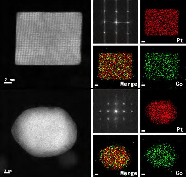
Researchers studying Pt3Co nanocatalysts aim to understand the crystalline changes that occur when annealed at 600°C for different lengths of time
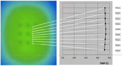
A unique, patented silicon carbide heating membrane ensures uniformity in the viewing area for accurate structure-temperature associations
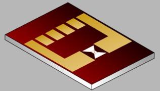

Fusion AX’s low-profile design maximizes line of sight to any EDS detector configuration
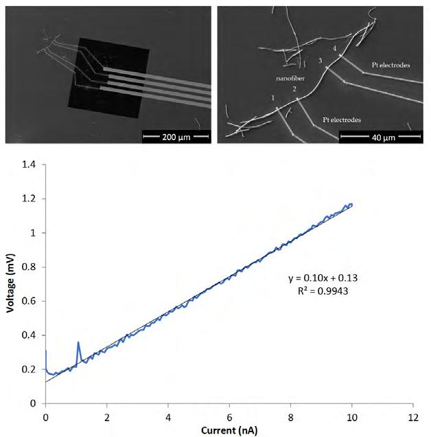
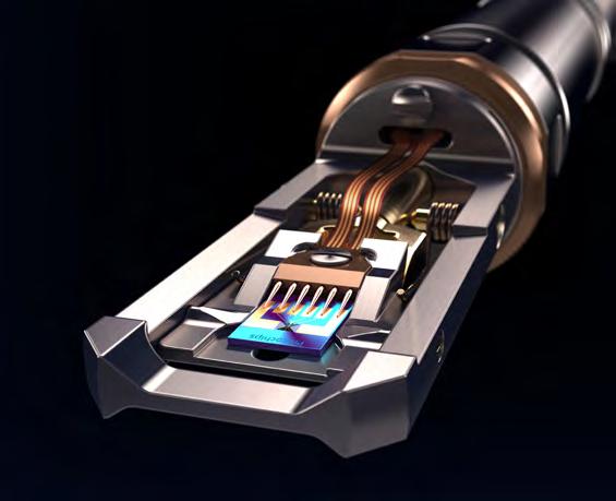
A unique silicon substrate on the sample supports ensures low electrical leakage and parasitics, enabling accurate electrical characterization of nanoscale samples
Researchers were able to collect electrical data relevant to a single titanium oxynitride nanofiber to better understand its conductivity for electrocatalytic applications, and correlated this back to bulk scale measurements. Smooth, linear measurements were obtained, even at low current and voltage levels.

Maximum electrical signal stability from friction-free double tilt mechanism, allows beta tilt while performing electrical measurements
Measure changes in electrical characteristics as a function of accurate temperature
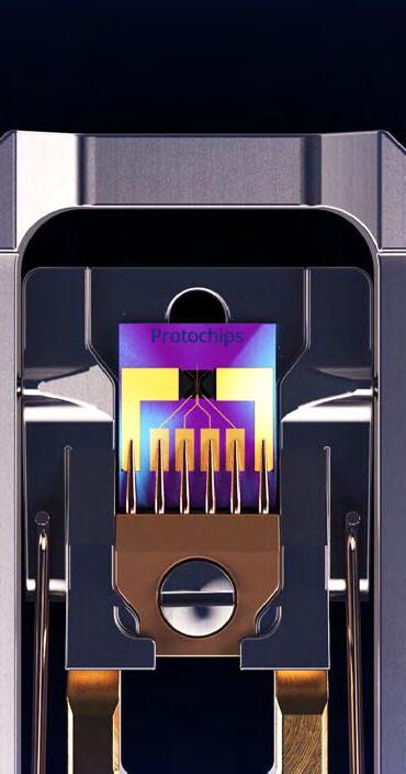

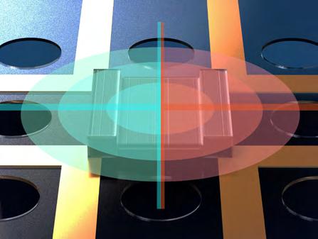
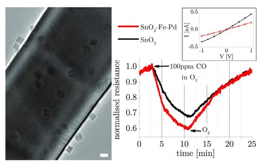
Researchers at the Okinawa Institute of Science and Technology in Japan used the electrothermal capability of Fusion, to visualize the structure change of SnO2 nanowires decorated with PdFe nanoparticles in response to CO exposure at elevated temperatures. Single SnO2 nanowire functionalized with Fe–Pd under 100 ppm CO in an E-TEM (scale bar 10 nm).
Electrical leads are placed on top of heating memebrane to ensure accurate temperature at the sample
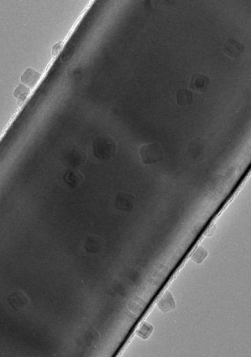
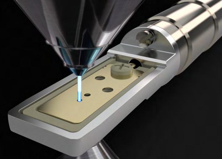
Accurate semi-automated beam current and area calibration with proprietary Faraday cup holder
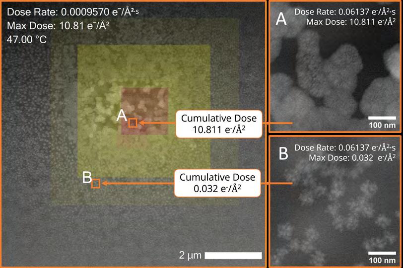
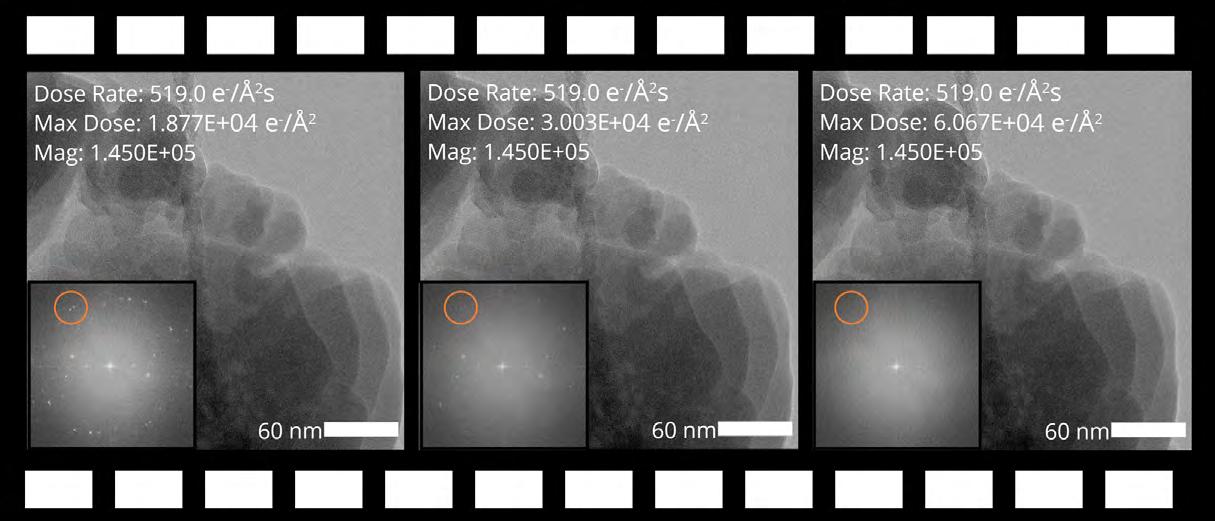
Once calibrated, the Dose software tracks electron exposure even as the sample moves. Electron exposure can be illustrated using colorful dose maps for quick visual understanding of accumulated dose
Thoughtfully designed arsenal of tools that support reproducible sample preparation and fast introduction into the TEM


Workflows to fit your sample
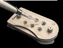
Drop-cast, sputtered & powder samples
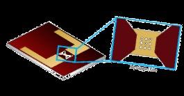
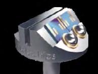


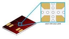
Clean, targeted sample preparation with a shadow mask ensures reproducible sample preparation from person to person.
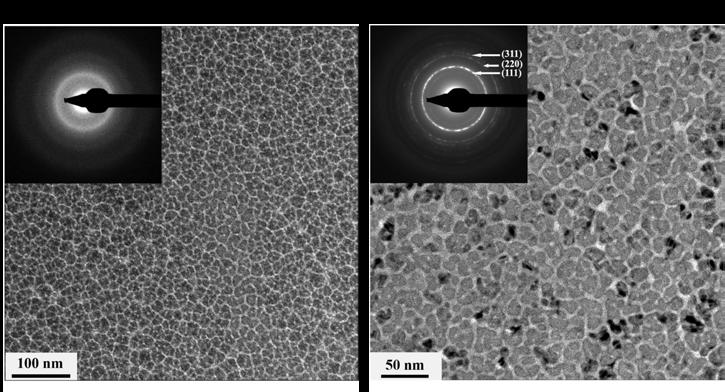
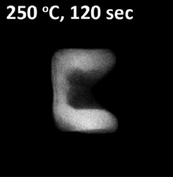
GST-225 (Ge2Sb2Te5) is a key active material in non-volatile phase-change memory devices.
Films were sputtered onto thermal E-chips to study the phase transformation of the material from amorphous to crystalline as a function of temperature.
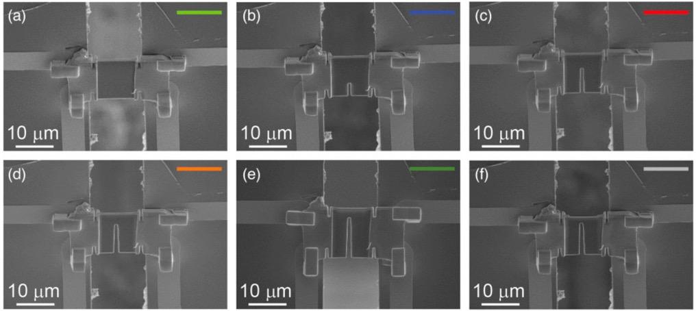


FIB-optimized E-chips, stub, and workflow enable FIB deposition with high success rate


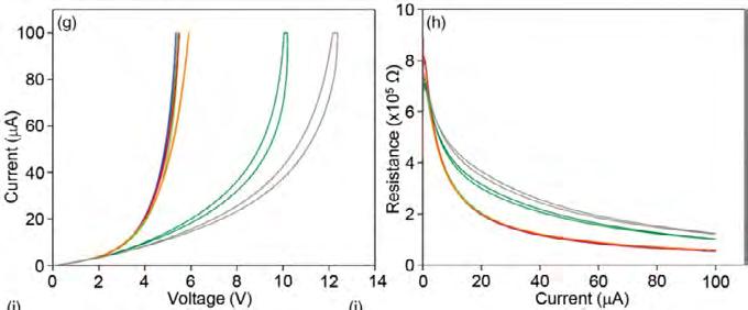
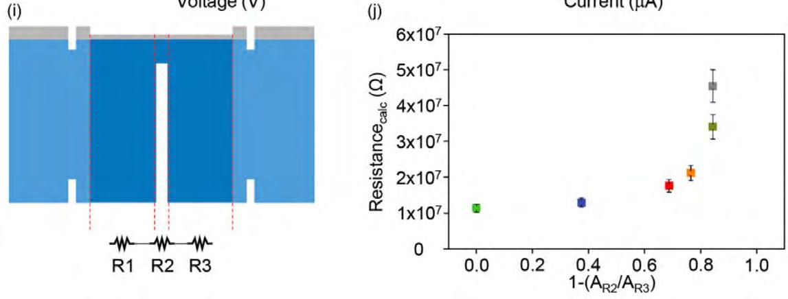


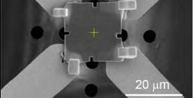
The design of a FIB lamella can have a large impact on its electrical characteristics. Here, researchers study the effect of notch length and lamella thickness on its current-voltage characteristics
AXON is a machine vision software platform with modular expansion for the TEM. AXON enables data collection and communication with the TEM and imaging systems, electron dose management, and large data set processing for reports and publication both inside and outside of the lab.
AXON provides a solution to help science return to a high level of rigor and reproducibility, and greatly enhances the productivity of scientific communication and collaborations.
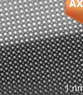
Obtain high resolution images much easier through machine vision stabilization technology | AXON SYNCHRONICITY
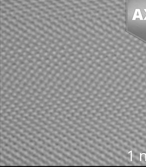

Live, 4-level drift correction technology continuously recenters and aligns the image throughout an experiment, even at high magnifications
Rough sample stage movements

Smaller piezo corrections Beam shifts for smaller drifts
More consistent, high-quality results for users of all experience levels
Digital correction is always on
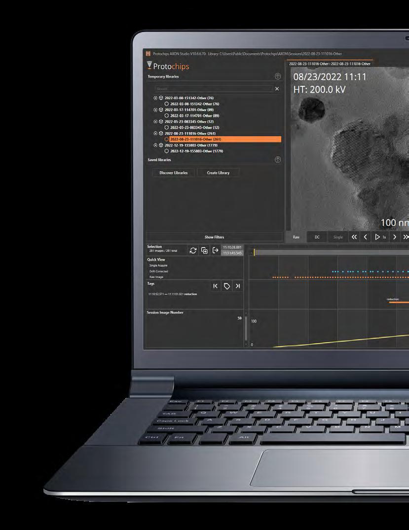
Visualize and navigate large amounts of data quickly and create reports
Include “session metadata” like notes, publications, and photos related to experimental preparation
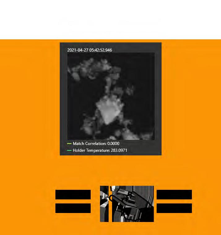
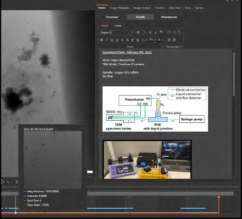
Filters and fast data scrubbing allow a quick review of very large image stacks to focus on the most important areas
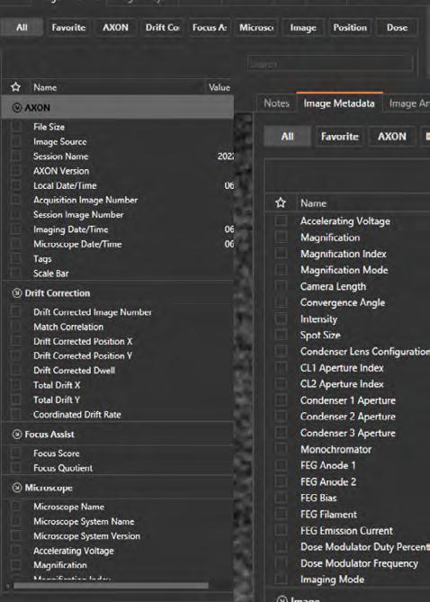
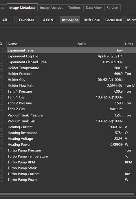
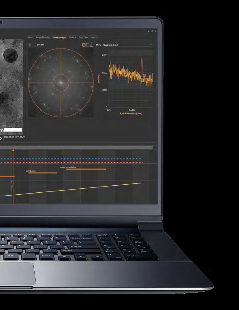
All metadata aligned with images in real-time…
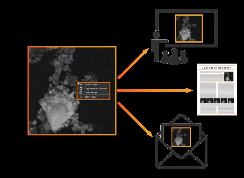
A simple copy/paste function builds reports in seconds, eliminating the need for complicated export processes and reformatting of data
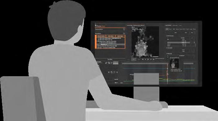
Identify trends and results much more easily in large data sets and across different instruments
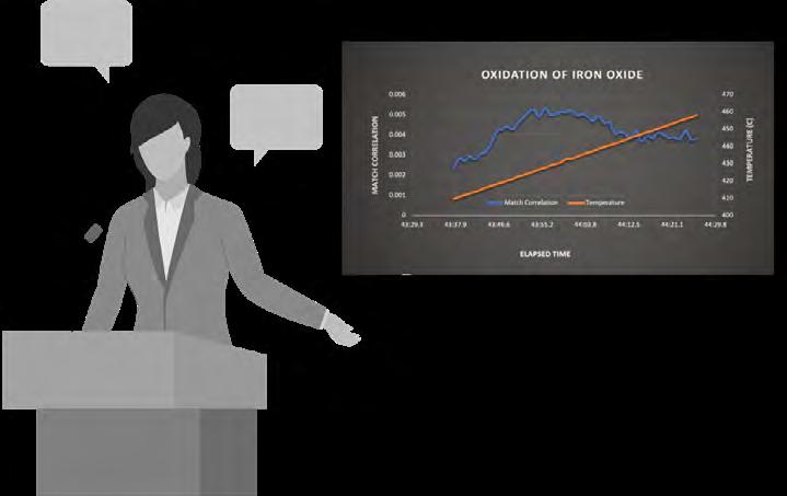
Enhance collaboration by making experimental results easier to share, publish and reproduce
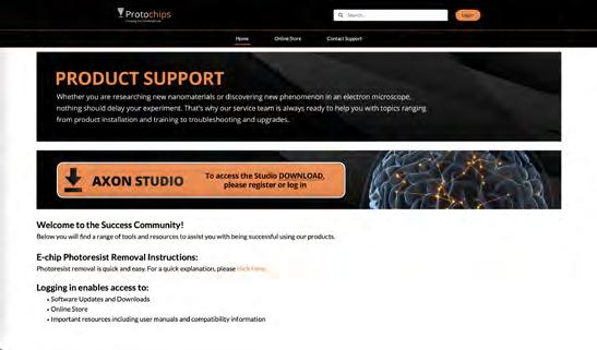
Studio is freely available to the community allowing data and metadata to be shared with anyone, greatly enhancing collaboration
All session and experimental history recorded, making correlation and reproduction of results far more accurate and quantitative, even between different instruments
All data continuously synchronized and indexed making it easy to sort, filter and analyze very large data sets
Conforms to the FAIR Principles Initiative – making data more Findable, Accessible, Interoperable and Reusable





FUSION AX FUSION AX FOR ELECTRONIC DEVICES FUSION AX PREMIERE
AXON Core
AXON Synchronicity Module with 2 year License x
AXON Dose Module with 2 year License x
AXON Dose Faraday Holder x
Fusion Select MEMS-based Heating Holder System x
Fusion Select MEMS-based Electrical Characterization
Holder System
Double Tilt Package
Electrothermal Capabilities


