EMBEDDED SYSTEM APPLICATIONS USING PIC18F4550
NORIAH BINTI MUSTAFA SHARMIZA BINTI KAMARUDDIN HELMI BIN JAMALUDIN
Editor PUZIAH BINTI YAHAYA Writer NORIAH BINTI MUSTAFA SHARMIZA BINTI KAMARUDDIN HELMI BIN JAMALUDIN Designer
Application Publishers and Developers Terbitan Edisi 2021
Copyright ©2021, by Politeknik Sultan Haji Ahmad Shah Materials published in this book under the copyright of Politeknik Sultan Haji Ahmad Shah. All rights reserved. No part of this publication may be reproduced or distributed in any form or by means, electronic, mechanical, photocopying, recording, or otherwise or stored in a database or retrieval system without the prior written permission of the publishers
Published by POLITEKNIK SULTAN HAJI AHMAD SHAH SEMAMBU 25350 KUANTAN Embedded System Applications Using PIC18F4550
i
ACKNOWLEDGMENT It is grateful to have a chance to contribute to this e-book project with guidance and countless help in every part of its production process. We like to express our gratitude for the supports of our family and friends.
ABSTRACT This e-book has developed based on a series of lectures notes used in the Embedded System Applications course in the Electrical Engineering Department, Polytechnic Sultan Haji Ahmad Shah (POLISAS). It contains eight chapters that parallel the syllabus of Embedded System Applications for Diploma of Electrical/Electronic Engineering in Polytechnics curriculum. This book covers the basic concept and application of a microcontroller system based on Peripheral Interface Controller (PIC) microcontroller. Students will learn software and hardware development on the PIC18F4550 microcontroller and understand how to do interface with external devices using suitable internal chip features. The variety of examples and review questions in this book may help students to have a better understanding of Embedded System Application using PIC18F4550.
ii
TABLE OF CONTENTS ACKNOWLEGEMENT
ii
ABSTRACT
ii
CHAPTER 1
1
INTRODUCTION TO EMBEDDED SYSTEM
1
1.1 Introduction
1
1.2 Real-Life Applications That Use Embedded System
1
1.3 Microcontroller Versus General-Purpose Microprocessor
2
1.3.1 Microprocessor
2
1.3.2 Microcontroller
3
1.5 The Advantages Of Microcontroller
5
1.6 Disadvantages Of Microcontroller
6
1.7 Microcontrollers Available In The Market
6
REVIEW QUESTIONS
7
CHAPTER 2
8
PIC PROGRAMMING IN C
8
2.1 Introduction
8
2.2 PIC18F4550 Microcontroller
8
2.3 Dual Role Of I/O Ports
9
2.4 Pic Programming In C
11
2.4.1 Compiler For Pic Microcontroller
11
2.4.2 Program Structure
12
2.4.3 C Data Types For The PIC18
13
2.4.4 Declaring Variable
14
2.4.5 Data Format In C
15
2.5 Byte & Bit I/O Programming
15
2.6 I/O PORT SFR Register
15
2.6.1 TRISx Register
17 iii
2.6.2 PORTx Register
18
2.6.3 LATx Register
19
2.7 LED (Light Emitting Diode)
20
2.8 Using Delay Function
23
2.9 Push Button Switch
26
REVIEW QUESTIONS
31
CHAPTER 3
32
PIC TIMER PROGRAMMING IN C
32
3.1 Introduction
32
3.2 PIC18F4550 TIMER
32
3.3 TIMER Register
34
3.3.1 TIMER0 Programming
35
3.3.2 TIMER0 Control Register (T0CON)
35
3.3.3 Prescaler
36
3.3.4 TMR0IF Flag Bit
38
3.4 Program TIMER0 To Generate Time Delay
39
3.4.1 STEPS TO PROGRAM TIMER0 TO GENERATE TIME DELAY
39
3.4.2 FINDING VALUES TO BE LOADED INTO TMR0H AND TMR0L
40
3.4.3 PRESCALER AND GENERATING A LARGE TIME DELAY
41
3.5 Programming TIMER0 As Counter
45
3.6 T0CON In Counter Mode
46
3.7 Step To Programming TIMER0 as Counter
47
REVIEW QUESTIONS
51
CHAPTER 4
52
INTERRUPT PROGRAMMING IN C
52
4.1 Introduction
52
4.2 Interrupt Vs Polling
52
4.3 Interrupt Service Routine (ISR)
53
iv
4.4 Sources Of Interrupts In PIC18
53
4.5 Bits To Control Interrupt Operation
54
4.6 Interrupt Registers
54
4.6.1 RCON - Reset Control Register
54
4.6.2 INTCON – Interrupt Control Register
55
4.6.3 INTCON2 - Interrupt Control Register 2
55
4.6.4 INTCON3 - Interrupt Control Register 3
56
4.7 Programming External Hardware Interrupt 4.7.1 Step To Enable External Hardware Interrupt
56 57
REVIEW QUESTIONS
63
4.8 Programming TIMER0 Interrupt
64
4.8.1 Program TIMER0 Interrupt to Perform Multitasking
65
4.8.2 Program TIMER0 Interrupt for Real Time Applications
68
REVIEW QUESTIONS
70
CHAPTER 5
71
BASIC ELECTRONIC CONNECTION
71
5.1 Minimum Electronics Connection Of Embedded System
71
5.1.1 Power Supply
71
5.1.2 Reset Circuit
72
5.1.3 Clock Signal
72
5.2 Digital Input Output In Pic
73
5.2.1 Digital Input
73
5.2.1.1 Active Low Input (Switch)
74
5.2.1.2 Active High Input (Switch)
74
5.2.2 Digital Output
75
5.2.2.1 LED
75
5.2.2.2 16X2 LCD Display
79
REVIEW QUESTIONS
89
v
CHAPTER 6
90
HARDWARE INTERFACING: ANALOG TO DIGITAL CONVERTER (ADC)
90
6.1 Analogue-To-Digital Converter (ADC)
90
6.2 PIC18F4550 ADC Features
90
6.3 PIC18F4550 ADC Registers
92
6.3.1 ADCON0 Register
92
6.3.2 ADCON1 Register
93
6.3.3 ADCON2 Register
94
6.3.4 ADRESH & ADRESL Register
95
6.4 Calculating A/D Conversion Time
96
6.5 Steps To Program ADC In PIC18
96
6.6 Sensor Interfacing and Signal Conditioning
98
6.6.1 LM35 Temperature Sensor
98
6.7 Reading And Displaying Analogue Value
100
REVIEW QUESTIONS
103
CHAPTER 7
105
HARDWARE INTERFACING: PULSE WIDTH MODULATION (PWM)
105
7.1 Pulse Width Modulation (PWM)
105
7.2 PIC18F4550 PWM
106
7.3 PWM Duty Cycle
106
7.4 PWM Register
108
7.4.1 PR2 Register
108
7.4.2 TIMER2 Control Register (T2CON)
109
7.4.3 CCP Control Register (CCPXCON)
110
7.4.4 CCPRXL Register
111
7.5 Steps For Programming
113
7.6 Application Of PWM
114
7.6.1 Application 1: Generating PWM Signal
114
7.6.2 Application 2: Control The Brightness Of LED Using PWM
116
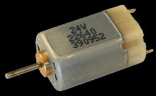
7.7 DC Motor
117 vi
7.7.1 L293D Motor Driver IC
118
7.7.2 Application 3: Control Dc Motor Speed Using PWM
120
REVIEW QUESTIONS
124
CHAPTER 8
125
HARDWARE INTERFACING: SERIAL COMMUNICATION
125
8.1 Serial Communication
125
8.1.1 PIC18F4550 UART
125
8.2 PIC18F4550 UART Register
126
8.2.1 SPBRG Register
126
8.2.2 BAUD RATE
126
8.2.3 TXSTA (Transmit Status And Control Register)
128
8.2.4 RCSTA (Receive Status And Control Register)
129
8.2.5 PIR1 (Peripheral Interrupt Request Register )
130
8.2.6 BAUDCON (Baud Rate Control Register)
131
8.3 Step To Program The PIC18 To Transmit Data Serially
132
8.4 Step To Program The PIC18 To Receive Data Serially
135
REVIEW QUESTIONS
137
CHAPTER 9
138
MINI PROJECT
138
9.1 Title: Dc Motor Control With PIC18F4550 and L293D (Proteus Simulation)
138
9.2 Circuit Diagram
138
9.3 Flow Chart
139
9.4 Programming
140
REFERENCES
146
vii
CHAPTER 1 INTRODUCTION TO EMBEDDED SYSTEM 1.1 Introduction
Embedded Systems are electronic systems within an equipment that contain a microprocessor or microcontroller, which are directly interfaced with input and output devices designed to perform a particular task.
“Embedded Systems are electronic systems that contain a microprocessor or microcontroller, but we do not think of them as computers – the computer is hidden or embedded in the system.” - Todd D. Morton author of Embedded Microcontrollers. Embedded system cannot be programmed by the user because it is preprogramed within the equipment which it serves.
1.2 Real-Life Applications That Use Embedded System
As consumer we use many applications that use embedded system such as Security system, automatic gate, answering machine, TV, VCR, Remote control, mobile phone, toys, smart cooker, microwave oven, automatic washing machine.
Embedded systems are not always standalone devices. Many embedded systems consist of small, computerized parts within a larger device that serves a more general purpose. Each of these peripherals has a microcontroller inside it that performs only one task.
A Personal Computer (PC) connected to various embedded products such as the keyboard, printer, modem, graphic card, mouse and so on. For example, inside every mouse a microcontroller performs the task of finding the mouse’s position and sending it to the PC. In a car many applications that use embedded systems - automotive safety systems include anti-lock braking system (ABS), Electronic Stability Control (ESC/ESP), traction control (TCS) and automatic four-wheel drive ,air bag, security system, keyless entry.
1
Airplanes contain advanced avionics such as inertial guidance system and GPS. Embedded system also used in RADARs, guided Missile System, automated guns and satellite phones.
1.3 Microcontroller versus general-purpose microprocessor
Processor is the heart of an embedded system. It is the basic unit that takes inputs and produces an output after processing the data. For an embedded system designer, it is necessary to have the knowledge of both microprocessors and microcontrollers.
1.3.1 Microprocessor
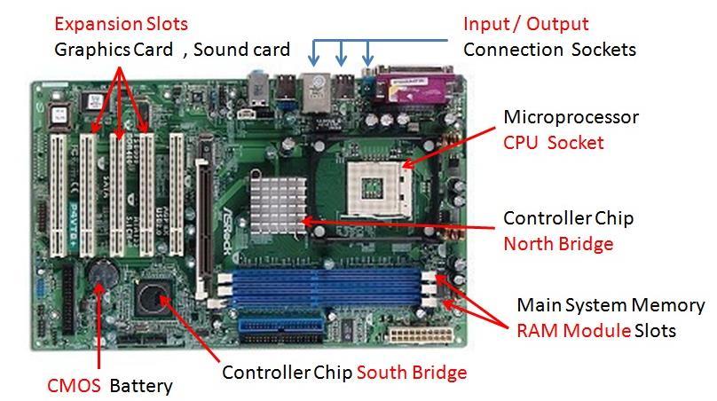
A microprocessor is a general-purpose processor with no external components attached to it. A microprocessor can perform various tasks depending on the user requirement. Some of the examples are web browsing, video gaming, sending emails, editing documents, etc. There are many microprocessors available that we use in modern computers and embedded system applications. Figure 1.1 shows different types of microprocessor chips.
Figure 1.1: Different type of microprocessor chips ( https://www.elprocus.com )
Therefore, we need to connect these peripherals with microprocessors according to the user requirement. We need to add I/O ports, serial communication ports, RAM, ROM and timers to a general-purpose processor to make it functional. The addition of these components makes systems more expensive and bulkier but they make a selection of systems more versatile. Because users can select RAM, ROM, input/output ports and other features
2
according to their requirement. An example of microprocessor applications is on computer motherboard as shown in Figure 1.2.
Figure 1.2: Component in computer motherboard (https://www.learncomputerscienceonline.com )
1.3.2 Microcontroller
A microcontroller (sometimes abbreviated µC, uC or MCU) is a single integrated circuit containing a processor core, memory, and programmable input/output peripherals. Microcontroller also called computer in chip. The fixed amount of on-chip ROM, RAM, and number of I/O ports in microcontroller makes them ideal for low cost and low space applications. Figure 3 shows the illustrations of inside of a microcontroller.
Figure 3: Inside microcontroller chip (https://www.polytechnichub.com)
3
Components inside microcontroller chip:
a.
CPU – Central Processing Unit (CPU) is the brain of the Microcontroller. A CPU reads, decodes and executes program to perform Arithmetic, Logic and Data Transfer operations.
b.
Memory – two types of Memory: Program Memory and Data Memory. Program Memory is used to store program source codes to be executed by the CPU. Data Memory is used to store temporary data while executing the instructions.
c.
Input/output (I/O) ports – interface for the Microcontroller to the external world. Inputs receive changes in the real-world, from sensor or push buttons, and much more provide information to the CPU. The CPU, upon receiving the data from the input devices, executes appropriate instructions and sends a signal to the output ports.
d.
Serial Ports – to communicate with other device and peripherals (external). Serial Port proves such interface through serial communication.
e.
Timers – provide the operations of Time Delays and counting external events.
f.
ADC (Analog to digital converter) – convert analog signals to digital.
g.
DAC (digital to analog converter) – supervise analog appliances like- DC motors, etc.
A microcontroller can perform only specific predefined tasks. Although a user can program it to perform any task. But once it is programmed, it can perform only specific tasks such as DC motor speed control, remote monitoring systems, etc. Figure 1.3 shows an example of application of microcontroller in embedded system.
Figure 1.3: Microcontroller chip in pen drive (https://steemit.com)
4
1.4 Differences between a microcontroller and microprocessor
The following are the major features to describe the difference between a microprocessor and microcontroller. Based on these aspects, we can clearly summarize the comparison between both digital integrated circuits.
Table 1.1: Differences between a microcontroller and microprocessor Aspect Internal Structure difference
Processing Speed
Microcontroller
Microprocessor
Support devices are
Must add RAM, ROM, I/O ports, and
internal for a
timers externally to make the
microcontroller
microprocessor functional.
Lower speed (in MHz range)
Higher speed (in GHz range)
Power
A microcontroller is used
Due to the high-speed processing
consumption
in low power and low-
requirement, the microprocessor
difference
speed applications
used more power consumption.
Cost Difference
Much cheaper and lower in cost
System more costly
Applications
Performs only one task
Perform various tasks
Software
Microcontrollers offer
Microprocessor based system fails to
protection
software protection
offer software protection system.
1.5 The advantages of microcontroller
a. support devices are internal – small system board b. Program is difficult to copy because of copy protection functions and an emulator will be required to copy it. c. Reduce chip count d. Many applications do not require as much computing power 5
1.6 Disadvantages of microcontroller
a. Can only do a specific task b. Limited amount of memory, I/O port and other internal features such as timers. c. Cannot add any external memory or I/O ports d. Different manufacturer using different internal architecture of microcontroller such as register and internal features
1.7 Microcontrollers available in the market
Today various types of microcontrollers are available in the market with different word lengths such as 4 bit, 8bit, 64 bit and 128-bit microcontrollers. There are several microcontroller architectures and vendors.
Table 1.2: Examples of vendor and microcontroller chips. Vendor ARM core processors (many vendors) Atmel Cypress Semiconductor Freescale Intel
Microchip Technology
Example of microcontroller chip ARM Cortex-M Atmel AVR (8-bit), AVR32 (32-bit), and AT91SAM (32-bit) PSoC (Programmable System-on-Chip) Freescale ColdFire (32-bit) and S08 (8-bit) Freescale 68HC11 (8-bit) Intel 8051 PIC, (8-bit PIC16, PIC18, 16-bit dsPIC33 / PIC24), (32-bit PIC32)
6
REVIEW QUESTIONS
1. Describe the meaning of embedded systems. 2. Describe the advantages of microcontroller application 3. List FOUR (4) common microcontrollers that available in the market 4. Identify THREE (3) examples of embedded system applications that are used in a car electronic system. 5. List THREE (3) embedded products attached to a personal computer.
7
CHAPTER 2 PIC PROGRAMMING IN C 2.1 Introduction
An embedded system is a combination of computer hardware and software designed for a specific function.
Embedded systems vary in complexity but, generally, consist of three main elements:
a. Hardware. The hardware of embedded systems is based around microprocessors and microcontrollers. Microprocessors are very similar to microcontrollers and, typically, refer to a CPU (central processing unit) that is integrated with other basic computing components such as memory chips and digital signal processors. Microcontrollers have those components built into one chip. b. Software and firmware. Software for embedded systems can vary in complexity. However, industrial-grade microcontrollers and embedded IoT systems usually run very simple software that requires little memory. c. Real-time operating system. These are not always included in embedded systems, especially smaller-scale systems. RTOSes define how the system works by supervising the software and setting rules during program execution.
2.2 PIC18F4550 Microcontroller
PIC microcontrollers are a family of specialized microcontroller chips produced by Microchip Technology in Chandler, Arizona. The acronym PIC stands for "peripheral interface controller". PIC18F4550 belongs to pic18f family of microcontrollers. There are different packages like DIP, QPF, and QPN of PIC18F4550 which are currently available as shown in Figure 2.1.
8
40 PIN Package DIP (Dual Inline Package)
44-Pin TQFP (Quad Flat Package)
44-Pin QFN (Quad-Flat No-leads)
Figure 2.1 PIC18F4550 chip Packages (https://www.microchip.com)
The PIC18F4550 is a 40-pins chip. A total of 33 are set aside for five ports: PORTA, PORTB, PORTC, PORTD and PORTE with their alternate functions which can be configured as input or output by setting registers associated with them. The rest of the pins are designated as Vdd, (Vcc), Vss (GND), OSC1, OSC2, MCLR (reset) and another set of Vdd and Vss. Figure 2.2 shows the pin diagram of PIC18F4550.
Figure 2.2: Pin diagrams for PIC18F4550 (https://www.theengineeringprojects.com)
2.3 Dual role of I/O Ports
Dual role of ports of data I/O is where a pin in PIC has more than one function. It can save more pins. In addition to being used as simple I/O, each port has some other functions such as ADC, timers, interrupts and serial communications pins.
By referring pins diagram in Figure 2.3, the port alternate function of each PIC’s pins can be seen next after the symbol “/” at the label.
9
For example, pin RA0/AN0 RA0 – used as input/output terminal for digital data (bit) AN0 – analogue-to-digital converter channel 0 (read analogue signal from external device).
Figure 2.3: Example of dual role I/O pin
Table 2.1 shows an example of I/O port alternate function.
Table 2.1: PORTA I/O Summary (Microchip PIC18F4550 Data sheet)
10
2.4 PIC Programming in C
It is not enough just to connect the microcontroller to other components and turn the power supply on to make it work. There is something else that must be done. The microcontroller needs to be programmed to be capable of performing anything useful. The following are the steps of programming an embedded system:
a. Write a program (example, using C language). b. Compile the program to convert it to machine language (in binary/hex). c. The program will be burned into a microcontroller chip using a special circuit called programmer/burner. d. Finally placed the microcontroller chip on the control circuit of the real application for example robot arm.
The illustration of these steps is shown in Figure 2.4.
Figure 2.4: Steps of programming an embedded system
2.4.1 Compiler for PIC microcontroller
When we write anything, then we write in C language which is a high level language, the computer or controller can’t understand this high-level language because it only understands the machine language. The Compiler, basically used to convert the high-level language into machine language or binary instructions.
11
The manufacturer supplies computer software for development known as MPLAB, assemblers and C/C++ compilers, and programmer/debugger hardware under the MPLAB and PICKit series. Microchip released their own C compilers, C18 and C30, for the line of 18F 24F and 30/33F processors. Other types of PIC compiler are MPLAB XC8 C Compiler, MPLAB XC16 C Compiler, MPLAB XC32 C Compiler, MikroC Compiler and PIC CCS Compiler
2.4.2 Program Structure
The structure of a C program is a protocol (rules) to the programmer, while writing a C program. The general basic structure of the C program is shown in Figure 2.5.
Figure 2.5: General basic structure of C program
There is no specific format in the writing program. Figure 2.6 shows an example of program structure in C language for PIC microcontroller.
12
Comments Include header file Include libraries, function declaration, global variable Main function name Begin of block Comments Local declaration
Function body
Figure 2.6: Example of program structure
End of block
User-defined Function
2.4.3 C Data Types for the PIC18
There are several types of data that can be used in C programming language. Data type is assigned to a variable to determine the size and how the variable is being interpreted as shown in Table 2.2. Table 2.2: Fundamental Data Types Type
Description
Bits
char
single character
8
Int
integer
16
float
single precision floating point number
32
double
double precision floating point number
64
In C programming language, there are various reserved words that can be used to modify the size or signage of an integer. Signed is rarely used because integers are signed by default. We
13
must specify unsigned if we want integers that are only positive. Possible combinations are shown in Table 2.3. Table 2.3: Modified Integer Types Data Type
Size in Bits
Data Range/Usage
unsigned char
8-bit
0 to 255
char
8-bit
-128 to +127
unsigned int
16-bit
0 to 655,535
int
16-bit
-32,768 to +32,767
unsigned short
16-bit
0 to 655,535
short
16-bit
-32,768 to +32,767
unsigned short long
24-bit
0 to 16,777,215
short long
24-bit
-8,388,608 to +8,388,607
unsigned long
32-bit
0 to 4,294,967,295
long
32-bit
-2,147,483,648 to +2,147,483,647
2.4.4 Declaring Variable
A variable must be declared before it can be used. The declaration of a variable consists of two parts:
a. A data types b. An identifier (or name) that will be used to uniquely identify the variable whenever we want to access or modify its contents.
The following are examples of C statement used to declare variable:
14
2.5 Byte & Bit I/O Programming
PIC18 registers are 8-bit registers, meaning that it can store 8-bit binary data. It can be access by 2 methods:
a. Byte-addressable change all 8 bits in the register Format: RegisterX = 0bxxxxxxxx
b. Bit-addressable Change single bit of register without altering the rest Format:
RegisterX = 0;
or
RegisterX = 1;
2.4.5 Data Format in C
The PIC microcontroller has only one data type. It is 8 bits, and the size of each register is also 8 bits. Data format is the way a value is being presented in C language. There are 4 ways to represent a byte of data. The numbers can be in hex, binary, decimal or ASCII formats as shown in Table 2.4.
Table 2.4: Data format Radix
Format
Example
Binary
0bnumber or 0Bnumber
PORTB = 0b01010101;
Octal
Onumber or \number
PORTB = O125;
Decimal
number
PORTB = 105;
Hexadecimal
0xnumber or 0Xnumber
PORTB = 0x55;
ASCII
‘character’
PORTD= ‘K’
15
2.6 I/O port SFR register
Each port of PIC microcontroller has three special function registers (SFR) for its operation. These registers are:
a.
TRISx register (data direction register)
b.
PORTx register (reads the levels on the pins of the device)
c.
LATx register (output latch)
These registers directly associated with the operation of the port, where 'x' is a letter that denotes the particular I/O port which is shown in Figure 2.7
Figure 2.7: PIC18 Special Function Register Map (Microchip PIC18F4550 Data sheet)
For example, for Port B we have PORTA, TRISA and LATA. Each register has 8 bits and each bit has a specific name as shown in Table 2.5 16
Table 2.5: Bits of TRISx, PORTx and LATx registers Bit
B7
B6
B5
B4
B3
B2
B1
B0
TRISA
-
-
TRISA5
TRISA4
TRISA3
TRISA2
TRISA1
TRISD0
PORTA
-
-
RA5
RA4
RA3
RA2
RA1
RD0
LATA
-
-
LATA5
LATA4
LATA3
LATA2
LATA1
LATD0
TRISB
TRISB7
TRISB6
TRISB5
TRISB4
TRISB3
TRISB2
TRISB1
TRISB0
PORTB
RB7
RB6
RB5
RB4
RB3
RB2
RB1
RB0
LATB
LATB7
LATB6
LATB5
LATB4
LATB3
LATB2
LATB1
LATB0
TRISC
TRISC7
TRISC6
PORTC
RC7
RC6
LATC
LATC7
TRISD PORTD
Register
LATD
-
-
-
TRISC2
TRISC1
TRISC0
RC5
RC4
-
RC2
RC1
RC0
LATC6
-
-
-
LATC2
LATC1
LATC0
TRISD7
TRISD6
TRISD5
TRISD4
TRISD3
TRISD2
TRISD1
TRISD0
RD7
RD6
RD5
RD4
RD3
RD2
RD1
RD0
LATD7
LATD6
LATD5
LATD4
LATD3
LATD2
LATD1
LATD0
TRISE
-
-
-
-
-
TRISE2
TRISE1
TRISE0
PORTE
-
-
-
-
-
PORTE2
TRISE1
TRISE0
LATE
-
-
-
-
-
LATE2
LATE1
LATE0
2.6.1 TRISx Register
The TRISx register control bits determine whether each pin associated with the I/O port is an input or an output: a. If the TRIS bit for an I/O pin is ‘1’, then the pin is configured as an Input. b. If the TRIS bit for an I/O pin is ‘0’, then the pin is configured as an Output.
For example, to configure the entire PORTD as input, all pins should be set to HIGH (1) as shown in Figure 2.8.
17
TRISD Value
Bit 7
Bit 6
Bit 5
Bit 4
Bit 3
Bit 2
Bit 1
Bit 0
1
1
1
1
1
1
1
1
TRISD = 0b11111111 = 0xFF
Figure 2.8: Bit configuration of TRISD register with PortD as input
Example 2.1 Refer to the circuit diagram in Figure 2.9. Assume the I/O devices are connected to PORTB. Write program statement to configure I/O port as input or output.
Solution: TRISB2 = 0;
//RB2 output
TRISB4 = 1;
//RB4 input
TRISB6 = 0;
//RB6 output
TRISB7 = 0;
//RB7 output Figure 2.9
Or
(https://www.mikroe.com)
TRISB = 0b00010000;
//RB4-input and RB2,RB6, RB7 - output
2.6.2 PORTx Register
PORTx registers hold the current digital state of the I/O pin. It reads the levels on the pins of the device and it assigns logic values (0/1) to the ports. The role of the PORT register is to receive the information from an external source (like a sensor) or to send information to the external elements (like an LCD).
When the port is used as the INPUT. The PIC can read signals from outside through PORT so we can determine which pins are currently HIGH or LOW.
18
When the port is used as the OUTPUT. The PIC can send signals outside through PORT. a. Write Logic 1 - PORTx registers will output 5V b. Write Logic 0 - PORTx registers will output 0V
Example 2.2 Write a program statement to output 5V to RB6 pin, 0V to RC2 pin and 5V to all pins of PortD. Solution: RB6 = 1; //5V to RB6 pin RC2=0; //0V to RC2 pin PORTD = 0b11111111; //5V to PortD. 2.6.3 LATx Register
LATx are the port latch registers. A write to a latch register is same as sending data to the port register PORTx. A read from the latch register, however, reads the data present at the output latch of the port pin, and this may not be same as the actual state of the port pin
The differences between the PORT and LAT registers can be summarized as follows:
A write to the PORTx register writes the data value to the port latch.
A write to the LATx register writes the data value to the port latch.
A read of the PORTx register reads the data value on the I/O pin.
A read of the LATx register reads the data value held in the port latch.
Example 2.3 Write a program code to output 0V to RB0-RB3 and 5V to RB4-RB7. Solution: LATB
bit 7
bit 6
bit 5
bit 4
bit 3
bit 2
bit 1
bit 0
Value
1
1
1
1
0
0
0
0
LATB = 0b11110000;
19
2.7 LED (Light Emitting Diode)
LEDs are a common element of many embedded designs. An LED, with a current limiting resistor, can be wired directly to one of the microcontrollers IO pins. An LED can be interfaced with a microcontroller in two different ways: in current source mode or current sinking mode. Figure 2.10 shows how to connect an LED in either 'sink' or 'source' modes:
a) The LED will light when the PIC pin is LOW.
b) The LED will light when the PIC pin is HIGH.
Figure 2.10: Interfacing of LED (http://www.winpicprog.co.uk)
In current source mode (Figure 2.10(b)), the microcontroller I/O pin is configured in the output direction. So, once the Logic "1" is at the output pin, then an LED will be turned "ON". And when Logic "0" is given the LED will be turned "OFF". See Figure 2.11
Figure 2.11: LED in source mode (https://aticleworld.com)
For LED in sink mode, when Logic "1" at output pin, then an LED will be turned "OFF". And when Logic "0" is given the LED will be turned "ON". 20
Example 2.4 A PIC18 based system interface with a LED which is connected to RD0. See Figure 2.12. Use bit addressable format to write a program code to perform as below: a)
configure RD0 as output pin
b)
On the LED (give Output 5V to RD0)
Solution: a) configure RD0 as output pin TRISD0=0; //RD0 as output pin b) On the LED (give Output 5V to RD0) RD0 = 1; //Output 5V to RD0
Figure 2.12
Example 2.5 A PIC18 based system interface with two LEDs which are connected to RD0 and RD7. See Figure 2.13. Use bit addressable format to write a program code to perform as below: a)
configure RD0 and RD7 as output pins
b)
give Ou tput 5V to RD0
c)
give Output 0V to RD7
Solution: a) configure RD0 and RD7 as output pin TRISD0=0; //RD0 as output pin TRISD7=0; //RD7 as output pin b) give Output 5V to RD0 and RD7 RD0=1; //Output 5V to RD0 OR LATD0=1; //Output 5V to RD0 c) give Output 0V to RD7 RD7=0; //Output 0V to RD7 OR LATD7=0; //Output 0V to RD7
Figure 2.13
21
Example 2.6 Refer to Figure 2.13, PIC18 based system interface with two LEDs which are connected to RD0 and RD7. Use byte addressable format to write a program code to perform as below: a)
configure RD0 and RD7 as output pins
b)
give Output 5V to RD0 and RD7
Solution: a) configure RD0 and RD7 as output pin TRISD0=0b00000000; b) give Output 5V to RD0 and RD7 PORTD=0b10000001;
//Output 5V to RD0 and RD7
OR LATD=0b10000001;
//Output 5V to RD0 and RD7
Example 2.7 By referring Figure 2.12, write a program to turn on the LED which is connected to pin RD0 of PIC18F.
Solution: #include <xc.h> void main(void) { TRISD0 = 0; while(1) { RD0 =1;
//turn on LED
} }
22
2.8 Using Delay function
A time delay is something that is very important when working with embedded applications, because there are times you want a delay before something is begun.
Time delays can also be used for breaks between processes. For example, a time delay in between an LED can make the LED blink on and off, on and off, repeatedly. So time delays can be very useful and important for embedded applications.
A __delay_ms() is not a real function, it is a macro which will expand into in-line assembly instructions or a nested loop of instructions which will consume the specified number of time. So the delay argument must be a constant and can't be changed during runtime. This function is known as the compiler’s in-built delay function.
If you want a real function with a parameter, you had to write it on your own as shown in Figure 2.14.
void delay_ms (unsigned int x) { for(; x>0; x--) __delay_ms(1); //delay 1ms } Figure 2.14: User defined delay function
If an accurate delay is required, or if there are other tasks that can be performed during the delay, then using a timer to generate an interrupt is the best way to proceed. The timer module of PIC will be discussed in the next chapter.
23
Example 2.8 Refer Figure 2.12, write a program to blink the LED which is connected to pin RD0 of PIC18. The LED will turn ON for 500 ms and turn OFF for 500 ms.
Solution: #include <xc.h> #define _XTAL_FREQ 20000000 #define LED RD0 void delay_ms (unsigned int x); void main(void) { TRISD0 = 0; while(1) { LED =1; //turn on LED delay_ms (500); //delay 500ms LED =0; //turn off LED delay_ms (500); //delay 500ms } } void delay_ms (unsigned int x) { for(; x>0; x--) __delay_ms(1); //delay 1ms } Example 2.9 By referring to Figure 2.13, LED1 is connected to RD0 and LED2 is connected to RD7. Write a program to make LED1 and LED2 blink alternately for each 2s continuously.
Solution: #include <xc.h> #define _XTAL_FREQ 20000000 #define LED1 RD0 #define LED2 RD7 24
void delay_ms (unsigned int x); void main(void) { TRISB = 0b00000000; //RD0 and RD7 as output pin while(1) { LED1 =1; //turn on LED1 LED2 =0; //turn off LED2 delay_ms (2000); //delay 2s LED1 =0; //turn off LED1 LED2 =1; //turn on LED2 delay_ms (2000); //delay 2s } } void delay_ms (unsigned int x) { for(; x>0; x--) __delay_ms(1); //delay 1ms } Example 2.10 You are assigned to design a running light using 8 LEDs. Assumed the LED is connected to PORTD as shown in Figure 2.15, write a complete program to make the LEDs turn on and off as below: 11000000 delay 1s 00110000 delay 1s 00001100 delay 1s 00000011 delay 1s
Use byte addressable format for data.
Figure 2.15
25
Solution:
#include <xc.h> #define _XTAL_FREQ 20000000 void delay_ms (unsigned int x); void main(void) { TRISD = 0b00000000; //PortD as output while(1) {
PORTD = 0b11000000; delay_ms(1000); PORTD = 0b00110000; delay_ms(1000); PORTD = 0b00001100; delay_ms(1000); PORTD = 0b00000011; delay_ms(1000);
// or LATD = 0b11000000; //delay 1s We can use shift operation (refer to appendix)
//delay 1s //delay 1s //delay 1s
}
PORTD = 0b11000000; delay_ms(1000); //delay 1s for (int y=0; y<3; y++) //repeat 3x { PORTD=PORTD>>2; // shift right PortD 2x delay-ms (1000); //delay 1s }
} void delay_ms (unsigned int x) { for(; x>0; x--) __delay_ms(1); //delay 1ms }
2.9 Push Button Switch
Push buttons are basic input device in an embedded system seen in very simple to highly complex systems. There two basic interfacing circuits of a push button switch: pull-up mode and pull-down mode.
26
In pull-up mode, the switch will be in active low configuration. See Figure 2.16. That is, the state of the pin is HIGH when the switch not pressed, and LOW when the switch is pressed.
Figure 2.16: Push button interfacing in pull-up mode (https://openlabpro.com)
In pull-down mode, the output acts as an active high. See Figure 2.17. The state of the pin is LOW when the switch not pressed, and HIGH when the switch is pressed.
Figure 2.17: Push button interfacing in pull-down mode (https://openlabpro.com)
27
Example 2.11 You are assigned to design a torchlight using a switch and a LED. The connection of the system is shown in Figure 2.18 Write a complete program for the system
Figure 2.18 Solution: #include <xc.h> #define SW RD1 #define LIGHT RB0 void main(void) { TRISD1 = 1; TRISB0 = 0; while(1) { if (SW == 0) // if SW is pressed { LIGHT = 1; //turn on LED } else { LIGHT = 0; //turn off LED } } }
28
Example 2.12 You are assigned to design a home security system using two switches and two LEDs. The switches is placed at the front door (SW1) and back door (SW2) of the home. The LEDs are used as indicator if the door is closed (switch is released) or open (switch is pressed). The connection of the system is shown in Figure 2.19. When SW1 is pressed, LED GREEN blink for 500ms and when SW2 is pressed, LED RED blink for 500ms. Write a complete program for the system.
Figure 2.19 Solution: #include <xc.h> #define SW1 RD1 #define SW2 RD7 #define LED_RED RB0 #define LED_GREEN RB1
void delay_ms (unsigned int x); void main(void) { TRISD = 0b10000001;
//RD0, RD7 as input pin
TRISB = 0b00000000;
//RB0, RB1 as output pin
PORTB=0;
//for initial – both LEDs off
29
while(1) { if (SW 1== 0)
// if SW1 is pressed
{ // LED GREEN blink for 500ms LED_GREEN = 1; delay_ms(250); LED_GREEN = 0; delay_ms(250); } else if (SW2 == 0) // if SW2 is pressed { // LED RED blink for 500ms LED_RED = 1; delay_ms(250); LED_RED = 0; delay_ms(250); } } } void delay_ms (unsigned int x) { for(; x>0; x--) __delay_ms(1); //delay 1ms }
30
REVIEW QUESTIONS
1. Write program code in C language for the following using byte addressable format: a. Initialize PORTA as an output b. Initialize RB0 and RB1 an input c. Output 5V to PORTD d. Output 0V to RB0 – RB4 and 5V to RB5 – RB7.
2. Write program code in C language for the following using bit addressable format: a. Initialize PORTA as an output b. Initialize RB0 and RB1 an input c. Output 0V to RA3 and RC1 d. Output 5V to RD1 and RB5
3. A programmer decides to make a control system that will control three LEDs and a buzzer. The LEDs and the buzzer were controlled by two digital sensors. Use any pins from PORTB for sensors, PORTC for buzzer and PORTD for LEDs, write program statement to configure pins as an input or output using bit addressable format.
4. A programmer decides to use two DC motors at pin RB6 and RB7. While, the LED at pin RA5 and two digital sensors at pin RB0 and RB1 in his circuit. Write the input output initialization for the program using byte addressable format in C language.
5. Build a C program to make LED1 on pin RD0 and LED2 on pin RD1 blink simultaneously for each 3 second continuously. The time delay function is given below: void Delay_1ms (unsigned int x) { for (; x>0; x--) __delay_ms(1); }
31
CHAPTER 3 PIC TIMER PROGRAMMING IN C 3.1 Introduction
Timers are common features of most microcontrollers. A timer is a register whose value keeps increasing (or decreasing) by a constant rate without the help of the CPU. Timers are used to generate time delay, counting events, generating waveform and also for PWM generation.
3.2 PIC18F4550 Timer
PIC18F4550 has four in-built timers named Timer0, Timer1, Timer2, and Timer3. Timer 2 is an 8-bit timer and all others are 16-bit timers.
The timer increments for each pulse applied to it. The timer counts continuously from 0 to (2n-1) where n is the number of bits. The initial values of the timer register can be set by the user and can be used to generate required counts. PIC18F4550 microcontroller has the following bit length (operation mode) of timer: a.
8 bit mode – count between 0 to 255 (28-1)
b.
16 bit mode – count between 0 to 65535 (216-1)
The timer operations mode for PIC18f4550 was simplified as shown in Table 3.1. while Figure 3.1 shows the Timers in PIC18f4550 block diagram.
Table 3.1: PIC18F4550 Timer Operation Mode Timer
Operation Mode 8-bit
16-bit
0
Yes
Yes
1
No
Yes
2
Yes
No
3
No
Yes
32
Figure 3.1: PIC18F4550 Block Diagram (Microchip PIC18F4550 Datasheet)
33
3.3 TIMER Register
Because the PIC18 has an 8-bit architecture, each 16-bit timer is accessed as two separate registers of low byte (TMRxL) and high byte (TMRxH). For example, Timer1 has TMR1H and TMR1L.
Each timer also has a TxCON (timer control) register for setting modes of operation. For example, T0CON is used to set modes for Timer0. All associated register with Timers in this microcontroller is illustrated in memory map in Figure 3.2.
Figure 3.2: Example of PIC18F4550 Timer Register Memory Map (Microchip PIC18F4550 Datasheet)
34
Embedded System Applications 3.3.1 TIMER0 Programming
Timer0 can be configured as an 8-bit or 16-bit timer or counter. The 16-bit register of Timer0 is accessed as low byte (TMR0L) and high byte (TMR0H) as shown in Figure 3.3. TMR0L
D15 D14
D13
D12
D11
TMR0H
D10
D9
D8
D7
D6
D5
D4
D3
D2
D1
D0
Figure 3.3: Timer0 High and Low Registers.
3.3.2 Timer0 Control Register (T0CON)
T0CON register controls the operation of Timer0. T0CON is an 8-bit register used for control of Timer0. The bits for T0CON are shown in Figure 3.4.
Figure 3.4: T0CON (Timer0 Control) Register 35
Embedded System Applications 3.3.3 Prescaler
A prescaler is an electronic counting circuit used to reduce a high frequency electrical signal to a lower frequency. The prescaler in PIC Timer is used to divide the CPU clock (Fosc/4) to obtain a smaller frequency. We can use the prescaler option in the TxCON register to increase the time delay by reducing the period. Figure 3.5 shows the simplified block diagram of Timer 0 module in PIC18.
Figure 3.5: Block diagram of Timer0 ( https://microchipdeveloper.com )
The prescaler is enabled by clearing the PSA bit of the T0CON register. In order to have a 1:1 prescaler value for the Timer0 module, the prescaler must be disabled by setting the PSA bit of the T0CON register. Figure 3.6 shows T0C0N register for PSA bit.
Prescaler Asignment 1: not assign to TMR0 0: assigned to TMR0
Figure 3.6: T0CON Register – PSA bit (Microchip PIC18F4550 Datasheet)
There are eight prescaler options for the Timer0 module ranging from 1:2 to 1:256. These prescaler are illustrated in Figure 3.7.
36
Embedded System Applications
TMR0 PRESCALE
PS2
PS1
PS0
0
0
0
1:2
0
0
1
1:4
0
1
0
1:8
0
1
1
1:16
1
0
0
1:32
1
0
1
1:64
1
1
0
1:128
1
1
1
1:256
VALUE
Figure 3.7: T0CON Register – Prescaler rate select bit (Microchip PIC18F4550 Datasheet)
Example 3.1 Find the value for T0CON if we want to program Timer0 in 16-bit mode, no prescaler. Use PIC’s Fosc/4 crystal oscillator for the clock source, increment on positive-edge. Solution: Refer T0CON register in Figure 3.4. TMR0ON
T08BIT
T0CS
T0SE
PSA
PS2
PS1
PS0
0
0
0
0
1
0
0
0
T0CON = 0000 1000 ;
//16-bit, Fosc/4 clock source, no prescaler, Timer0 off.
Example 3.2 If T0CON = 0b11000100, determine timer operation modes of TIMER0 Solution: 1 Enable TMR0
1 8 bit mode
0
0
0
Internal
Low-high
Use
clock
transition
prescaler
1
0
1
1:32 prescaler
T0CON : operation modes: 8-bit mode (refer bit-6). 37
Embedded System Applications 3.3.4 TMR0IF flag bit
TMR0IF bit (Timer0 interrupt flag) is part of the INTCON (interrupt control) register that will be discuss further on Chapter 4. Figure 3.8 shows the INTCON Register that associated with TMR0IF. 0: Timer0 did not overflow 1: Timer0 has overflowed
Figure 3.8: INTCON Register – Timer0 interrupt flag (Microchip PIC18F4550 Datasheet)
The TMR0IF interrupt is generated when the TMR0 register overflows from FFh to 00h in 8bit mode, or from FFFFh to 0000h in 16-bit mode. For example, when a 16-bit timer has the value 65535 (FFFF H) and receives another clock that will set it to 0 and generate an overflow as illustrated in Figure 3.9.
XTAL OSCILLATO R
TMR0H
÷4
TMR0IF (OVERFLOW FLAG
TMR0L
TMR0ON
FFFF ----- > 0000 TMR0IF = 0---- > TMR0IF = 1
Figure 3.9: TIMER0 Overflow flag
The importance of TMR0IF: a.
In 16-bit mode, when TMR0H:TMR0L overflows from FFFFH to 0000H this flag is raised.
b.
In 8-bit, it is raised when the timer goes from FFH to 00H.
c.
We monitor this flag before we reload the TMR0H:TMR0L registers
The block diagram in Figure 3.10 Figure 3.10 shows the operation of Timer0 16-bit mode: 38
Embedded System Applications
Figure 3.10: Block diagram of Timer0 operation 16 bit mode ( Microchip PIC18F4550 Datasheet)
3.4 Program TIMER0 To Generate Time Delay
To generate a time delay using Timer0, we have to calculate a count of desired time. The following are the steps to program Timer0 to generate time delay.
3.4.1 Steps to program Timer0 to generate time delay
a.
Load the value into theT0CON register indicating which mode (8-bit or 16-bit), internal clock source and the selected prescaler option.
b.
Load initial count value into register TMR0H followed by register TMR0L. (for 8bit mode we can only use TMR0L)
c.
Start the timer with instruction “TMR0ON= 1”
d.
Keep monitoring the timer flag (TMR0IF) to see if it is raised. Get out of the loop when TMR0IF becomes HIGH. Example of instruction, “while (TMR0IF==0);”
e.
Stop the timer with instruction “TMR0ON= 0”
f.
Clear the TMR0IF flag for the next round.(TMR0IF=0)
g.
Go back to Step 2 to load TMR0H and TMR0L again.
39
Embedded System Applications We should load TMR0H first and then load TMR0L because the value for TMR0H is kept in a temporary register and written to TMR0H when TMR0L is loaded. This will prevent any error in counting if the TMR0ON flag is set HIGH.
Program code using Timer0 to generate time delay (16-bit mode): T0CON=0b_____ ; TMR0H=0x_____; TMR0L=0x_____; TMR0ON= 1; while(TMR0IF== 0); TMR0ON= 0; TMR0IF= 0;
// Configure the T0CON register // initial count values (high byte). // initial count values (low byte). // Start the timer // Keep monitoring the TMR0IF to see if it is raised // Stop the timer //Clear TMR0IF
Program code using Timer0 to generate time delay (8-bit mode): T0CON=0b______; TMR0L=0x_____; TMR0ON= 1; while(TMR0IF== 0); TMR0ON= 0; TMR0IF= 0;
// Configure the T0CON register // initial count values // Start the timer // Keep monitoring the TMR0IF to see if it is raised // Stop the timer //Clear TMR0IF
3.4.2 Finding values to be loaded into TMR0H and TMR0L The following are the steps to calculate the values to be loaded into TMR0H and TMR0L registers:
a. Find the time for one clock period (Tc): TC = 1/ (FOSC /4/prescaler) s b. Calculate the number of count (NOC) to get the required time delay: NOC = Time Delay = Td Time Period Tc c. Get the value to be loaded into TMR0: i. TMR0 = 65535 – count + 1 ii. TMR0= 255 – count + 1
(16-bit mode) or TMR0 = 65536 – count (8-bit mode) or TMR0= 256 – count 40
Embedded System Applications d. Convert this value to hexadecimal, we get 0xYYXX e. Load this hex value in the Timer0 : TMR0H = 0xYY TMR0L= 0xXX. **(For 8-bit mode, put the result into TMR0L)
3.4.3 Prescaler and generating a large time delay The time delay generated using Timer depends on two factors. a. The crystal frequency b. The timer’s 16-bit register
Both of these factors are beyond the control of the PIC18 programmer. The largest time delay is achieved by making both TMR0H and TMR0L zero.
We can use the prescaler option in the T0CON register to increase the delay by reducing the period. The prescaler option of T0CON allows us to divide the instruction clock by a factor of 2 to 256.
Example 3.3 Find the largest time delay possible using Timer 0 if the system uses crystal oscillator frequency 10MHz.
Solution: To get the largest time delay, use: 16-bit mode : NOC = 65536 (need 65536 clock pulse to tick) Prescaler: 256 (maximum prescaler)
Fc = Fosc/4 / prescaler
= (10 MHz /4 ) / 256
= 9.766 KHz
Clock period, Tc = 1 / Fc
= 1 / (9.766 KHz)
= 102.4 µs
Time delay = NOC x Tc = 65536 x 102.4 µs = 6.72 s 41
Embedded System Applications In real time applications, we use time delay in seconds or milliseconds or microseconds. The following are examples of how to calculate the real time used.
Example 3.4 Assuming XTAL = 10 MHz and no prescaler . Find the TMR0H and TMR0L registers values if we want to get a time delay 1ms.
Solution:
Timer clock freq,
Fc=Fosc/4= 10MHz/4=2.5MHz.
Timer clock period,
Tc= 1/Fc=1/2.5MHz=0.4us
NOC = Td / Tc = 1ms / 0.4us = 2500 ticks (>255, use 16-bit mode) Value loaded into TMR register
= 65536 – 2500 = 63036 = F63C (hex)
TMR0H =F6 (Hex) TMR0L=3C. (Hex)
Example 3.5 Assuming that XTAL=10 MHz, write a program to generate a square wave with a period of 10ms on pin RB3. The output produce as shown in Figure 3.11.
Figure 3.11 Solution: For square wave with T= 10ms, we must divide period into two for high and low state. Time delay use to produce high and low state:
42
Embedded System Applications Td = T / 2 = 10ms/2 = 5ms Fc = Fosc/2 =10MHz / 2 = 5MHz Tc= 1/Fc = 15MHz = 0.4 µs. NOC = 5ms / 0.4 µs = 12500 ticks. TMR0 register value = 65536 – 12500 = 53036 = CF2C (Hex). Therefore, TMR0H = CF and TMR0L = 2C.
Program: #include <xc.h> void delay_5ms( ); void main (void) { ADCON1=0b00001111; TRISB3=0; while (1) { RB3 =1; delay_5ms( ); RB3 =0; delay_5ms( ); }
// RB3 as output
//output logic HIGH (5V) to RB3 //delay 5ms //output logic LOW (0V) to RB3 //delay 5ms
} //function for time delay 5ms void delay_5ms( ) { T0CON=0b00001000; //Configure timer 10MHz crystal, 16-bit mode, no prescaler TMR0H=0xCF; TMR0L=0x2CF; TMR0ON= 1; // Start the timer while(TMR0IF== 0); // Keep monitoring the TMR0IF to see if it is raised TMR0ON= 0; // Stop the timer TMR0IF= 0; //Clear TMR0IF }
43
Embedded System Applications Example 3.6 Refer to the schematic in Figure 3.12, construct a program to blink LED1 every 500ms. Use Fosc 10MHz and prescaler 1:64.
Figure 3.12 Solution: Fc = Fosc/4/64 = 10MHz /4/64 = 39.0625 kHz Tc = 1/Fc = 1/ 39.0625 kHz = 25.6µs NOC = Td / Tc = 500ms / 25.6µs =19531 ticks TMR0 value = 65536 – 19531 = 46005 = B3B5 (hex) Program: #include <xc.h> #define LED1 RD0 void delay_500ms( ); void main (void) { ADCON1=0b00001111; TRISD0=0; while (1) { LED1 =1; delay_500ms( ); LED1 =0; delay_500ms( ); }
//turn on LED 1 //delay 500ms //turn off LED 1 //delay 500ms
}
44
Embedded System Applications
//function for time delay 500ms void delay_500ms( ) { T0CON=0b00000101; //Configure timer for10MHz crystal, 16-bit mode prescaler 1:64 TMR0H=0xB3; TMR0L=0xB5; TMR0ON= 1; while(TMR0IF== 0); // Keep monitoring the TMR0IF TMR0ON= 0; // Stop the timer TMR0IF= 0; //Clear TMR0IF } 3.5 Programming Timer0 as Counter
Timers are also used as counters to count events happening outside the microcontroller. Example application of counter is Measuring the RPM (speed in revolution per minute) of the rotating wheel. A small magnet is attached in the edge of the wheel as shown in Figure 3.13. Whenever this magnet is exactly below the Magnetic sensor its output becomes high. This output is connected to the T0CKI (Timer0 Clock Input) pin of the MCU. So each time the magnet passes by the sensor the timer register inside the MCU is incremented. These all happen without the help of CPU. CPU can do other task and read the Timer register only when required. The system connected as shown in Figure 3.13.
Figure 3.13: Example application of counter (https://extremeelectronics.co.in)
45
Embedded System Applications 3.6 T0CON in Counter mode
Timer0 will be program as counter by selecting external clock source. mode is selected by setting timer T0CS bit in the T0CON register as in Figure 3.14. TMR0 CLOCK SOURCE SELECT 1: T0CKI 0: FOSC/4
Figure 3.14: Bit T0CS of T0CON register (Microchip PIC18F4550 Datasheet)
In PIC18, the clock pulse is fed through T0CKI (RA4) and T1CKI (RC0) pins. See Figure 3.15. The T0CS bit in the (Timer0 clock source) in the T0CON register decides the source of the clock for the timer. When T0CS=1, the timer is used as a counter and gets its pulse from outside the PIC18.
Figure 3.15: T0CKI (RA4) and T1CKI (RC0) pins
The counter will increment either on rising or falling edge of the clock pulses, which is selectable by the T0SE (Timer0 Source Edge) as in Figure 3.16.
46
Embedded System Applications
SOURCE SELECT EDGE SELECT BIT: 1: INCREMENT HIGH TO LOW 0: INCRTEMENT LOW TO HIGH
Figure 3.16: Bit T0CE of T0CON register (Microchip PIC18F4550 Datasheet)
The range of the counter can be extended by the use of the prescaler. Example 3.7 Find the value for T0CON if we want to program Timer0 as an 8-bit mode counter, no prescaler. Use an external clock for the clock source and increment in the positive edge. Solution: T0CON=0b01101000;
//8-bit, external clock source, n0 prescaler.
3.7 Step to programming Timer0 as counter The following are step to program Timer0 as counter: a.
Configure T0CON register.
b.
Set initial value of counter.
c.
Start timer
d.
Wait for TMR0IF to raised (Timer roll over)
e.
Stop timer
f.
Clear TMR0IF
Finding values to be loaded into TMR0H & TMR0L a.
16-bit mode ( if count value > 255): TMR0 = 65535 – NOC + 1
b.
or
TMR0 = 65536 – NOC
Convert this value to hexadecimal, we get 0xYYXX TMR0H = 0xYY and TMR0L= 0xXX.
c.
8-bit mode ( count value <= 255): TMR0L = 255 – NOC + 1
or
TMR0L = 256 – NOC 47
Embedded System Applications Example 3.8 Assume that a 1 Hz external clock is fed into pin T0CKI (RA4). Referring to Figure 3.17, write a C program for counter0 in 8-bit mode to count up and display the state of TMR0L count on PORTB which is connected to 8 LEDs. Start the count at 0H. PORTB .
PORTB
To all LEDs 1 Hz T0CKI
RA4
Figure 3.17 Solution:
#include <xc.h> void main void { ADCON1=0X0F; TRISA4=1 TRISB=0; T0CON=0x68; TMR0L=0; while (1) { do { TMR0ON=1; PORTB=TMR0L; }
//make RA4/T0CKI an input //counter 0, 8-bit mode, no prescaler //set count to 0 //repeat forever
//turn on T0 //place value on PORTB pins
while (TMR0IF==0); //wait for TF0 to roll over TMR0ON=0; //turn off T0 TMR0IF=0; //clear TF0 } }
48
Embedded System Applications Example 3.9 As a programmer you are assign to develop a counter system to count the number of cars entering to a parking area. The control system use a digital sensor is connected to pin T0CKI and buzzer is connected to pin RB1 as Figure 3.18, Write a program using Timer0 in 8-bit mode to sound the buzzer every time 100 cars enter the parking area.
RB1
BUZZER
RA4
100 Hz
T0CKI
PIC18F
Figure 3.18
Solution: The buzzer will turn on after timer count 100 pulses (overflow). The value needs to put into TMR0L register: to start count N= 255-100 +1 = 156 = 9C (Hex) TMR0L=156; or TMR0L=0x9C; Program:
#include <xc.h> void main void { ADCON1=0X0F; TRISA4=1
//make RA4/T0CKI an input
TRISB1=0; T0CON=0x68;
//counter 0, 8-bit mode, no prescaler
TMR0L=156;
//start count at 156
49
Embedded System Applications while (1)
//repeat forever
{ TMR0ON=1;
//turn on T0
while (TMR0IF==0);
//wait for TF0 to roll over
TMR0ON=0;
//turn off T0
TMR0IF=0;
//clear TF0
RB1= 1;
// turn on the buzzer
delay_ms (100); RB1= 0;
// turn off the buzzer
TMR0L=156;
//reconfigure the counter value
} }
50
Embedded System Applications REVIEW QUESTIONS
1.
Construct a function for void delay (void) in C language to generate a 1 second delay by using 20Mhz Fosc, 16 bit mode and prescale 1:256.
2.
The following is a schematic diagram for a conveyor system for loading tennis ball into a box as in Figure 3.19. Each box can be load NINE (9) tennis balls. A sensor is used to detect the tennis ball that fall into the box. When all the balls fall into the box, the LED will turn on for 2 second. By using Timer0 as counter, write a program to perform the operation.
1st 2nd ball ball
9th ball RA4
RD4
PIC18F 4550
Figure 3.19: Tennis Conveyor system
51
Embedded System Applications
CHAPTER 4 INTERRUPT PROGRAMMING IN C 4.1 Introduction
Interrupt is a signal sent by peripheral or software to a processor that requires the CPU to stop the current program execution and run a specific program to perform some service related to the event. The program associated with the interrupt is called the interrupt service routine (ISR) or interrupt handler.
4.2 Interrupt vs Polling
A single microcontroller can serve several devices. There are two methods by which devices receive service from the microcontroller: Interrupt or polling.
Table 4.1: Comparison between Interrupt and Polling Interrupt
Polling
Whenever any device needs the
Microcontroller continuously monitors the
microcontroller’s service, the device notifies it
status of a given device; when the status
by sending an interrupt signal. Upon receiving
condition is met, it performs the service.
an interrupt signal, the microcontroller stops
After that, it moves to monitor the next
whatever it is doing and serves the device.
device until each one is serviced.
The advantage of interrupt is that the
Polling method cannot assigned priority
microcontroller can serve many devices (not all
because it checks all the devices in round-
at the same time). Each device can get the
robin fashion
attention of the microcontroller based on the priority assigned to it. Interrupts are used to avoid tying down the
Polling method wastes much of
microcontroller.
microcontroller’s time by polling devices that do not need service.
52
Embedded System Applications 4.3 Interrupt Service Routine (ISR)
For every interrupt, there must be an interrupt service routine (ISR) or interrupt handler. ISR tells the processor or controller what to do when the interrupt occurs. When an interrupt is invoked, the microcontroller runs the interrupt service routine.
Figure 4.1: Interrupt Service Routine
4.4 Sources of Interrupts in PIC18
There are many sources of interrupts in the PIC18. The following are some of the most widely used source of interrupts in the PIC18:
1. External hardware interrupt , at pins RB0, RB1 and RB2 for INT0, INT1 and INT2 respectively. 2. The PORTB-Change interrupt 3. Timer interrupt (Timer 0, 1, 2 and 3 ) 4. Serial communication’s USART interrupt, transmit and receive.. 5. The ADC (analog-to-digital converter). 6. The CCP (compare capture pulse-width-modulation)
The PIC18 has many more interrupts than the above list shows.
53
Embedded System Applications 4.5 Bits to Control Interrupt Operation
In general, each interrupt source has the following related bits.
Table 4.2: Bits to Control Interrupt Operation Bits
Function They are suffixed with IE (Interrupt Enable) for example, TMR0IE
Enable Bit
stands for TIMER0 Interrupt Enable. It can be used to enable/disable the related interrupt. When set to ‘1’ it enables the interrupt. It is set automatically by the related hardware when the interrupt condition occurs. It is generally suffixed with IF (Interrupt Fag). When it
Flag Bit
is set to ‘1’ we know that an interrupt has occurred. For example when TMR0IF is set by TIMER0, it indicates that TIMER0 has overflowed. Multiple interrupts could occur at the same time but since our
Priority Bit
microcontroller is single core it can process only one interrupt at a time. Priority bit is used to prioritize some interrupts over others.
GIE
Global interrupt Enable, enable/disable interrupt globally
PEIE
Enable/disable all peripheral interrupt
4.6 Interrupt Registers
PIC18F4550 has ten registers which are used to control interrupt operation. These registers are RCON, INTCON, INTCON2, INTCON3, PIR1, PIR2, PIE1, PIE2, IPR1, IPR2
4.6.1 RCON - Reset Control Register
Table 4.3: Reset Control Register Bit 7
Bit 6
Bit 5
Bit 4
Bit 3
Bit 3
Bit 2
Bit 0
IPEN
SBOREN
—
RI
TO
PD
POR
BOR
IPEN: Interrupt Priority Enable bit. Enables priority levels when set. 54
Embedded System Applications 4.6.2 INTCON – Interrupt Control Register
Table 4.4: Interrupt Control Register Bit 7
Bit 6
Bit 5
Bit 4
Bit 3
Bit 3
Bit 2
Bit 0
GIE/GIEH
PEIE/GIEL
TMR0IE
INT0IE
RBIE
TMR0IF
INT0IF
RBIF
GIE/GIEH: Global Interrupt Enable bit When IPEN is disabled, GIE enables all interrupts When IPEN is enabled, GIEH enables all high priority interrupts PEIE/GIEL: Peripheral Interrupt Enable bit When IPEN is disabled, PEIE enables all peripheral interrupts When IPEN is enabled, GIEL enables all low priority interrupts TMR0IE: TMR0 Overflow Interrupt Enable bit. Enables the TMR0 overflow interrupt INT0IE: INT0 External Interrupt Enable bit. Enables the INT0 external interrupt RBIE: RB Port Change Interrupt Enable bit. Enables the RB port change interrupt TMR0IF: TMR0 Overflow Interrupt Flag bit. Sets when TMR0 register has overflowed INT0IF: INT0 External Interrupt Flag bit. Sets when INT0 external interrupt occur RBIF: RB Port Change Interrupt Flag bit. Sets when at least one of the RB7: RB4 pins change state
4.6.3 INTCON2 - Interrupt Control Register 2
Table 4.5: Interrupt Control Register 2 Bit 7
Bit 6
Bit 5
Bit 4
Bit 3
Bit 3
Bit 2
Bit 0
RBPU
INTEDG0
INTEDG1
INTEDG2
—
TMR0IP
—
RBIP
INTEDGx: External Interrupt x Edge Select bit. If set, the Interrupt flag is set on the rising edge. If cleared Interrupt flag is set on falling edge
55
Embedded System Applications TMR0IP: TMR0 Overflow Interrupt Priority bit. If set, TMRO interrupt is set as a High priority interrupt RBIP: RB Port Change Interrupt Priority bit. If set, RB Port Change Interrupt is set as a High priority interrupt
4.6.4 INTCON3 - Interrupt Control Register 3
Table 4.6: Interrupt Control Register 3 Bit 7
Bit 6
Bit 5
Bit 4
Bit 3
Bit 3
Bit 2
Bit 0
INT2IP
INT1IP
—
INT2IE
INT1IE
—
INT2IF
INT1IF
INTxIP: INTx External Interrupt Priority bit. If set, INTx External Interrupt is set as a High priority interrupt INTxIE: INTx External Interrupt Enable bit. Enables the INTx external interrupt INTxIF: INTx External Interrupt Flag bit. The bit sets when INTx external interrupt occurs
4.7 Programming External Hardware Interrupt
There are three external hardware interrupts in PIC18: INT0, INT1 and INT2. They are located on pins RB0, RB1 and RB2, respectively. See Figure 4.2
Figure 4.2: External Hardware Interrupt Pins 56
Embedded System Applications External interrupts pins are edge-triggered. If the corresponding INTEDGx bit in the INTCON2 register is set (= 1), the interrupt is triggered by a rising edge; if the bit is clear, the trigger is on the falling edge. When a valid edge appears on the RBx/INTx pin, the corresponding flag bit, INTxIF, is set. Table 4.7: External Interrupt Register Interrupt
Flag Bit
Register
Enable Bit
Register
INT0 (RB0)
INT0IF
INTCON
INT0IE
INTCON
INT1 (RB1)
INT1IF
INTCON3
INT1IE
INTCON3
INT2 (RB2)
INT2IF
INTCON3
INT2IE
INTCON3
4.7.1 Step to enable External Hardware Interrupt
1. The following are steps to enable External Hardware Interrupt: 2. Enable Global Interrupt Enable bit (GIE) Bit D7 of the INTCON register must be set to HIGH. 3. Enables the INTx external interrupt. 4. Set INTxIF to LOW. 5. Set condition caused interrupt (falling/rising edge). 6. Set interrupt priority for INT1 and INT2. There is no priority bit associated with INT0. It is always a high-priority interrupt source.
Example 4.1 Write program code to enable external hardware interrupt on RB0 (INT0). Assume the interrupt will occur when RB0 changes from HIGH to LOW .
Solution GIE=1;
// Enable Global Interrupt Enable bit (GIE.)
INT0IE=1;
//Enables the INT0 external interrupt
INT0IF=0;
//clear interrupt flag
INTEDG0=1; // interrupt on rising
57
Embedded System Applications Step to write Interrupt Service Routine (ISR):
1. Declare function "void interrupt ISR()“. The words "interrupt" in the function causes it becomes as Interrupt Service Routine (ISR) when an interrupt occurs. 2. Check the related interrupt flag. Example: if (INT0IF==1) //check if INT0 interrupt occurs. 3. Write operation for the related interrupt 4. Clear the related interrupt flag. Example: INT0IF=0; //clear INT0 interrupt flag
Example of ISR:
void interrupt ISR() { if(INT0IF==1) //check if INT0 interrupt occurs { Write operation for the related interrupt } INT0IF=0;
//clear INT0 interrupt flag
}
Example 4.2 A push button (active high) is connected to RB0 (INT0) and a LED is connected to RD0 of PIC18. Write a program so that, every time INT0 is activated, LED is toggled
Solution //Toggled a LED using INTERRUPT #include <xc.h> //Interrupt Service Routine (ISR) void interrupt ISR();
58
Embedded System Applications void main (void) { TRISB0=1; TRISD0=0; ADCON1=0x0F; //Enable Interrupt Register GIE=1;
// Enable Global Interrupt Enable bit (GIE.)
INT0IE=1; //Enables the INT0 external interrupt INT0IF=0;
//clear interrupt flag
INTEDG0=1; // interrupt on rising edge; while(1); //Wait }
void interrupt ISR() { if ( INT0IF==1 ) { LATD0=LATD0^1;
//Toggle LED
} INT0IF=0;
//Clear Interrupt Flag, ready for next interrupt
}
Example 4.3 A control system uses a LED and digital sensor as Figure 4.3. In normal condition, the LED will turn off. If the switch is pressed, the LED on RA2 will blink 3 times. Write a program for the control system using external hardware interrupt.
59
Embedded System Applications
Figure 4.3 Solution #include <xc.h> #define LED RA2 void interrupt ISR(); void main (void) { TRISB1=1; TRISA2=0; ADCON1=0x0F; //Enable Interrupt INT0 GIE=1; INT1IE=1; INT1IF=0; INTEDG1=0; while(1) { LED=0; }
// Enable Global Interrupt Enable bit (GIE.) //Enables the INT0 external interrupt
//loop forever
}
void interrupt ISR() { if ( INT1IF ==1 ) { for(int i=0;i<3;i++) 60
Embedded System Applications { LED= 1; __delay_ms(300); LED= 0; __delay_ms(300);
//Turn on LED //delay 300ms //Turn off LED //delay 300ms
} } INT1IF=0;
//Clear Interrupt Flag, ready for next interrupt
} Example 4.4 Refer to Figure 4.3. TWO (2) switches are connected to RB0 (INT0) and RB1 (INT1). While two LEDs are connected to RB3 and RB4. Write a program using interrupt method to read the status of SW1 and SW2. When the SW1 is pressed, LED1 will turn on and LED will turn off. Otherwise, when SW2 is pressed, LED1 will turn off and LED2 will turn on. The interrupt is triggered by a falling edge of the pulse.
Figure 4.3
Solution #include <xc.h> #define LED1 RB2 #define LED2 RB3 void interrupt ISR();
61
Embedded System Applications void main (void) { TRISB=0B00000011; ADCON1=0x0F;
//Enable Interrupt at INT0 GIE=1;
// Enable Global Interrupt Enable bit (GIE.)
INT0IE=1;
//Enables the INT0 external interrupt
INT0IF=0;
//clear interrupt flag
INTEDG0=0;
// interrupt on falling edge;
//Enable Interrupt at INT1 INT1IE=1;
//Enables the INT1 external interrupt
INT1IF=0;
//clear interrupt flag
INTEDG1=0;
// interrupt on falling edge;
INT1IP=1;
//Enables the INT1 interrupt priority
while(1);
//Wait
}
//Interrupt Service Routine (ISR) void interrupt ISR() { if (INT0IF ==1) { // turn on LED 1 and turn off LED2 LED1= 1; LED2= 0; INT0IF=0;
//Clear INT0IF
}
62
Embedded System Applications if (INT1IF ==1) { // turn off LED1 and turn on LED2 LED1= 0; LED2= 1; INT1IF=0; //Clear INT1IF, } }
REVIEW QUESTIONS
1. List sources of interrupts in the PIC18 microcontroller. 2. Explain the steps to enable External hardware interrupt on RB0 (INT1) 3. Explain the steps to enable External hardware interrupt on RB0 (INT2) 4. PIC microcontroller is connected to a lamp via pin RC0, while LDR is connected to pin RB1. When the voltage across the LDR becomes zero volts, the lamp will turn on. Write a program using an interrupt method.
5. A wood cutting machine in a factory does not have safety features. To improve the safety feature of the machine, you are assigned to develop a safety system using an infrared sensor which is used to detect the presence of the hand. When an object (hand) is detected, the machine will stop immediately. Design the safety system by using a PIC18 microcontroller with suitable I/O devices. Sketch a schematic diagram for the system and write a program for the control system. 63
Embedded System Applications 4.8 Programming Timer0 Interrupt
In the previous chapter we use a timer to generate time delay. The delay loops will pause our program. We have to wait until the timer flag is raised when the timer rolls over. The problem with this method is that the microcontroller is tied down waiting for TMR0IF to be raised, and cannot do anything else.
Using interrupt avoids tying down the controller. The best thing about timer interrupts is that they work in the background and we don’t have to wait for them. When they finish work, they will produce an interrupt. It is like an alarm clock. In this chapter we will use hardware timer interrupt to perform multitasking and real-time application.
Figure 4.4: Timer Interrupt logic diagram
INTCON – Interrupt Control Register
Table 4.8: Interrupt Control Register
Interrupt priority for Timer0 is determined by the value contained in the interrupt priority bit, TMR0IP (INTCON2).
64
Embedded System Applications INTCON – Interrupt Control Register
Table 4.9: Interrupt Control Register 2
a. Step to enable timer interrupt b. Setup T0CON (timer mode, clock source, prescaler) c. Set the TMR0 preload value d. Enable Timer 0 interrupt enable bit e. Clear TMR0IF f. Enable Global Interrupt Enable bit g. Enable Peripheral Interrupt Enable bit for Timer1 and Timer 2.
Example of program code to enable Timer0 interrupt:
T0CON=0b___________; TMR0L=0x_____;
// Configure the T0CON register // preload value TMR0H & TMR0L
TMR0H=0x_____; GIE=1;
// Enable Global Interrupt Enable bit
TMR0IE=1;
// Enable Timer 0 interrupt enable bit
TMR0IF=0
// Clear TMR0IF
PEIE=1;
// Enable Peripheral Interrupt Enable bit for Timer1 and Timer 2.
4.8.1 Program Timer0 Interrupt to Perform Multitasking Using Timer0 interrupt, we can program PIC microcontroller to perform multitasking. In this approach, the delay is provided by loading a count in a timer. When a timer interrupt is generated current execution will move to the ISR to serve the task. But when there is no timer interrupt it will perform another task. 65
Embedded System Applications Example 4.4 Refer to the following Figure 4.5. Write a C program using Timer0 interrupt to turn on and off a buzzer every delay 3 second and LED every delay of 2 second. At the same time, data is being transferred from PORTC to PORTD. Use crystal frequency 8MHz, 16 bit mode and pre-scale of 1:32.
Figure 4.5
Solution:
Fc = 8MHz/4/32 = 62.5 kHz Tc = 1/ 62.5 kHz = 16 us Count = 1s / 16 us = 62500 TMR0 register = 65536- 62500 = 3036 = 0BDC (Hex) TMR0H=0x0B; TMR0L=0xDC;
Program:
#include <xc.h> void interrupt ISR (void); unsigned int tmr_LED, tmr_buz;
66
Embedded System Applications void main (void) { ADCON1=0b00001111; TRISB1=0; TRISB7=0; TRISC=0xFF; TRISD=0x00;
//RB1 : output //RB7 : output //PORTC : input // PORTD : output
//configure timer to activate TMR0IF every 1 s T0CON=0b00000100; //Timer0, 16-bit mode, prescaler 1:32 TMR0H=0x0B; TMR0L=0xDC; //Enable timer 0 Interrupt GIE=1; TMR0IE=1; TMR0IF=0; TMR0ON=1; while(1) { PORTD=PORTC; }
//transfer data from PORTC to PORTD
} //Interrupt Service Routine (ISR) void interrupt ISR (void) { if (TMR0IF==1) { tmr_LED = tmr_LED +1; tmr_buz = tmr_buz +1; if (tmr_LED ==2) { RB1=~RB1; tmr_LED =0; }
// time = 2 x 1s = 2s //toggle LED
67
Embedded System Applications
if (tmr_buz == 3) { RB7=~RB7; tmr_buz =0; }
// time = 3 x 1s = 2s //toggle buzzer
//restore TMR0H & TMR0L value TMR0H=0x0B; TMR0L=0xDC; TMR0IF=0; //clear TMR0IF } }
4.8.2 Program Timer0 Interrupt for Real Time Applications We can use timer interrupt programming to perform real time applications, for example, a counter system.
Example 4.5
A fruit packaging factory wants to install an automatic packaging system. The system used two DC motors to move two conveyor belts. The first conveyer belt is used to carry and drop the fruits into boxes and the second conveyor belt is used to move a box. A sensor is used to detect the fruits that fall into the box. When 50 of the fruits have fallen into the box, the fruit conveyor belt will stop and the second conveyor will move for 2 seconds to place a new empty box.
Sketch the control circuit using PIC18 microcontroller, and write a program using Timer0 Interrupt as a counter to perform the operation. Use any pins as output.
68
Embedded System Applications Solution Schematic diagram
Program : #include <xc.h> #define Motor1 RB3 #define Motor2 RB5 void interrupt ISR (void); void main (void) { ADCON1=0b00001111; TRISA4=0; TRISB3=0; TRISB5=0; //configure timer as counter T0CON=0b01101000; TMR0L=206; //Enable timer 0 Interupt GIE=1; TMR0IE=1; TMR0IF=0; TMR0ON=1; while(1) { Motor1=1; Motor2=0; } }
//RA4 : input //RB3 : output //RB5 : output // 8-bit mode, clock source from RA4, no prescaler //set count value to 50, (255 -50 +1)
//turn on motor 1 // turn off motor 2
69
Embedded System Applications
//Interrupt Service Routine (ISR) void interrupt ISR (void) { if (TMR0IF==1) { Motor1=0; Motor 2=1; delay_ms(2000); TMR0L=206; TMR0IF=0; } }
//turn off motor 1 //turn on motor 2 //restart timer //clear TMR0IF
REVIEW QUESTIONS
1. Explain the steps to enable Timer0 interrupt 2. You are assigned to build a running LED using a PIC microcontroller. Develop a C program using Timer0 interrupt to get the following LED transition: a.
The first LED (RA0) blink every 100ms
b.
Second LED (RA1) blink every 200ms
c.
The third LED (RA2) blink every 400ms
70
Embedded System Applications
CHAPTER 5 BASIC ELECTRONIC CONNECTION 5.1 Minimum electronics connection of embedded system
Minimum hardware connection so that the PIC microcontroller can operate and make microcontroller function is you need to give a DC power supply, a reset circuit and a reset circuit and a quartz crystal (system clock) from external source. The basic connection of embedded system as in Figure 5.1.
POWER SUPPLY
CLOCK SIGNAL
RESET CIRCUIT
Figure 5.1: Basic connection of an embedded system
5.1.1 Power Supply
Microcontroller only need a minimum 3v or 5V DC and this power supplies are commonly used in embedded systems.
71
Embedded System Applications 5.1.2 Reset Circuit
Reset circuit consists of a push button and resistor, connecting the reset pin (MCLR) used to restart the system.
Figure 5.2: Reset Circuit of PIC microcontroller
5.1.3 Clock Signal
Clock signal is used to execute microcontroller instructions. Clock signal is supplied through the external OSC pin of the microcontroller. However modern microcontrollers come with both external and internal ( built-in) oscillators.
Examples of external clock sources are as below and the connection as Figure 5.3: a.
crystal oscillator
b.
Resonator.
c.
RC circuit
Figure 5.3: Clock Signal Circuit
72
Embedded System Applications Table 5.1 : Mode, frequency and capacitor for clock signal circuit MODE LP
XT
HS
FREQUENCY
C1,C2
32KHz
33pF
200KHz
15pF
200KHz
47-68 pF
1 MHz
15pF
4MHz
15pF
4MHz
15pF
8MHz
15-33 pF
20MHz
15-33 F
5.2 Digital I/O voltage level
In embedded systems, a microcontroller must be interfaced with input and output (I/O) devices to make it useful. The state of I/O devices can be programmed. Digital I/O state should be in logic “LOW” or logic “HIGH” in any given time.
Table 5.2 : Digital input and output voltage levels LS-TTL INPUT
VOLTAGE VALUES
VOLTAGE
LS-TTL OUTPUT
VOLTAGE
VOLTAGE
VALUES
LOGIC 1
5V
LOGIC 1
2.7 – 5V
NOT USABLE
0.8 - 2.0V
NOT USABLE
0.4V-2.7V
LOGIC 0
0- 0.8V
LOGIC 0
0 – 0.4V
5.3 Digital Input
Switch is a commonly used component to give digital signals. Examples of digital input devices are toggle switch, LDR, thermistor, micro-switch.
73
Embedded System Applications
Figure 5.3: Digital input device (https://tech.alpsalpine.com)
5.3.1 Active LOW input (switch)
It is being connected in pulled high configuration; the input signal is initially set to 5V (high). When the switch is pressed, the input signal becomes 0V (low). In the program, please check for logic low (0V) if a press is needed.
PIC18F4550
Figure 5.3: Active LOW input circuit
5.3.2 Active HIGH input (switch)
The opposite condition happened to the pulled low configuration. R1 is a pull down resistor holding the PIC pin at logic “0”. Pressing the switch connects the PIC input to the 5V rail, forcing it to logic “1”. 74
Embedded System Applications
PIC18F45 50
Figure 5.4: Active HIGH input
Besides switches, digital sensors also provide digital signals to microcontrollers which serve the same function as switches.
5.4 Digital Output
Examples of output devices are LED, buzzer, bulb, speaker, motor, solenoid, etc. Below is an example of output devices used in embedded system applications.
Figure 5.6: Digital output device(http://archive.fabacademy.org)
5.4.1 LED
LED is the most basic and commonly used output device in electronic circuit boards. It is an indicator that we can use to display the logic status (High or Low) of a specific pin.
75
Embedded System Applications Connecting the LED without a resistor is likely to damage both the LED and the PIC. To calculate the resistor needed for a simple LED circuit, simply take the voltage drop away from the source voltage then apply Ohm's Law. where:
VS - source voltage, measured in volts (V), VLED - voltage drop across the LED, measured in volts (V), ILED - current through the LED*, measured in Amperes (Amps/A), and R - the resistance, measured in Ohms (Ω). * The current through the circuit is constant so ILED is also the current through the resistor.
Example 5.1 A 3mm red LED has a forward voltage drop of 2.1V and at 20mA output, R = 5V – 2.1V = 145 Ω
(use the higher resistor value)
20 mA
As like other output devices, LEDs can be active-high or active-low.
5.4.1.1 Active HIGH output (source) “Source” is the I/O pin is the actual source of the current, and it flows out of the pin through the load down to ground as in Figure 5.7. The LED will light up when the PIC pin is high.
Figure 5.7: Active-high connection
76
Embedded System Applications 5.4.1.2 Active LOW output (sink) “Sink” means that the chip “sinks” current down into itself, so the load is connected from the positive rail to the I/O pin and the load is switched ON by the pin going “LOW’ as in Figure 5.8. The LED will light up when the PIC pin is low.
Figure 5.7: Active-low connection
5.4.2 Buzzer
Same as the LED, buzzer is a simple output component that can be used as a sound indicator when there is an emergency. The buzzer will buzz continuously when power is provided (5V) and will shut down when the power is being cut off (0V). In other words, this is an active high configuration. Refer to Figure 5.8 for the connection of buzzer with PIC Microcontroller.
Figure 5.8: Connection of buzzer to PIC microcontroller
77
Embedded System Applications Example 5.2 Sketch a complete circuit for a control system that uses the PIC18F4550 microcontroller interface with a switch (active LOW) connected to RC0 and a LED (active LOW) connected to RB6.
Solution
Example 5.3 A control system use PIC18f4550 microcontroller connected to a switch (active Low) and a LED (active High). The switch is connected to pin RD3 and the LED is connected to pin RB1. Sketch a schematic diagram for control system. Solution:
78
Embedded System Applications 5.4.3 Relay
Relay is an electrical device that is used as a switch in an electrical system with high current or voltage. In direct connection, a microcontroller is unable to provide or resist large current and voltage. However, using Relay, the microcontroller is able to control connection with high current and voltage. Figure 5.5 shows the circuit connection between relay and microcontroller with high current and voltage
.
Figure 5.5: Relay to control connection with high current and voltage
5.4.4 16X2 LCD Display
2x 16 LCD Display is specifically manufactured to be used with microcontrollers, which means that it cannot be activated by standard IC circuits. It displays all the letters of the alphabet, Greek letters, punctuation marks, mathematical symbols etc. In addition, it is possible to display symbols made up by the user. 16 x 2 LCD display can display messages in two lines with 16 characters each. Figure 5.7 refers to how 16x2 LCD display, while Table 5.3 show the pin description for 16x2 LCD LM016L.
79
Embedded System Applications We can control a LCD using either 8 pins (8-bit interface) or 4 pins (4-bit interface), depending on the I/O pins that we have. For learning purposes, we would recommend 8-bit interface which is relatively easy. Table 5.3 show the pin description 2x16 LCD.
Figure 5.7: 16x2 LCD display (https://www.instructables.com)
Table 5.3: Pin Description 2x16 LCD PINS
FUNCTION
1
GROUND
2
VCC
3
VEE-CONTRAST VOLTAGE
4
RS: INSTRUCTION/REGISTER SELECT
5
R/W: READ/WRITE REGISTER
6
E: CLOCK
7-14
DATA INPUT/OUTPUT
15-16
LCD BACKLIGHT
Table 5.4: LCD Command Control Code (https://electronicswork.blogspot.com)
80
Embedded System Applications E-clock
The E pin requires a “High” to “Low” pulse to latch in information at the data pins of a LCD. The pulse period at ‘E’ pin as shown in Figure 5.8.
Figure 5.8: 16x2 LCD Enable pin and pulse (https://www.electronicwings.com)
Set Cursor Position
Setting up cursor position is an important part of LCD which defines at which index (column and row) we want to display text. As we know we are using 16×2 alphanumeric LCD means 16 columns and 2 rows, index shown in figure 5.9.
Figure 5.9: LCD 16×2 Index (https://pijaeducation.com)
The LCD contains a certain amount of memory which is assigned to the display represented with the following "memory map“: Each position has their own address. 81
Embedded System Applications The numbers in each box is the memory address that corresponds to that screen position.
The first character of line 1 is at address 00h. This continues until we reach the 16th character at address 0Fh.The first character of line 2, is at address 40h. The last position of the first line at address 4Fh. Figure 5.10 shows the DDRAM address in hex for 2x16 LCD Display.
Figure 5.10: LCD 16×2 DDRAM Address (https://electronicswork.blogspot.com)
Command to jump to address for display must start with 0x80, because the bit7 must be set (1).We need to send a command to the LCD that tells it to position the cursor on the other position. To change the cursor to another position on the LCD we must add the address of the location where we wish to position the cursor. 2 ways to add address:
1. 0x80 | Address 2. 0x80 + Address
Command registers and Data register in LCD display:
a. Command Register
The command register stores the command instructions to do a predefined task like initializing it, clearing its screen, setting the cursor position, controlling display etc. Table 5.4 shows LCD command control code.
82
Embedded System Applications b. Data Register
The data register stores the data to be displayed on the LCD. The data is the ASCII value of the character.
5.4.4.1 Programming step Before using the LCD for display purpose, LCD has to be initialized either by the internal reset circuit or sending the commands to initialize the LCD. The following programming steps explain the procedure of configuring the LCD and display a character on it.
Step 1: Initialize the LCD
The LCD must be initialized by the following pre-defined commands of character LCD: a. 0x38, to configure the LCD for 2-line, 5x7 font and 8-bit operation mode b. 0x0C, for Display on and Cursor Off c. 0x01, to Clear Display screen d. 0x06, to increment cursor e. 0x80, to set cursor position at first block of the first line of LCD The above set of commands is written in ” lcd_initialize() “ function of the adjoining code.
Step 2: Send the commands to LCD.
Send the command byte to the port connected to LCD data pins:
a. RS=0, to select command register of LCD b. R/W=0, to set the LCD in writing mode. c. EN=1, a high to low pulse to latch command instruction d. Delay of 1ms e. EN=0
83
Embedded System Applications Step 3: Send data to LCD
Send data at the port which connected to LCD data pins: a. RS=1, register select to select data register of LCD b. RW=0, this set the LCD in writing mode c. EN=1, a high to low pulse to latch data d. Delay of 1ms e. EN=0,
The lcd_data(unsigned char) function has the above set of instructions.
Other LCD functions. From lcd-command and lcd_data, we can create other user defined function as below:
a.
lcd_setCursor() – set cursor position
b. put_ch() - send a character to be displayed on LCD c.
put_str( ) - send a string to be displayed on LCD
Example 5.4 Write a command to clear the LCD display.
Solution: LCD command to clear display is binary 000000001 (refer “LCD Command table”). LCD_RS=0;
//select command register
LCD_DATA=0b00000001;
//clear LCD display
LCD_E = 1;
// set E clock to HIGH
delay_ms(2);
// delay 2ms
LCD_E = 0;
// falling of E clock to LOW
delay_ms(2);
// delay 2ms
84
Embedded System Applications Example 5.5 Write instruction to send character ‘A’ to LCD display
Solution: LCD_RS=1; LCD_DATA=‘A’; LCD_E = 1;
// set E clock to HIGH
delay_ms(2);
// delay 2ms
LCD_E = 0;
// falling of E clock to LOW
delay_ms(2);
// delay 2ms
Example 5.6 Write a program to initialize LCD display as below:
Solution: LCD_E=1;
//LCD initialize
delay_ms(10); LCD_RS=0; LCD_DATA=0x38; e_clock(); LCD_DATA=0x06; e_clock(); LCD_DATA=0x0F; e_clock(); LCD_DATA=0x01; e_clock();
85
Embedded System Applications
Example 5.7 The following are examples of sub-functions of LCD displays. void lcd_initialize(void) { LCD_E=1; delay_ms(10); LCD_RS=0; LCD_DATA=0x38; e_clock(); LCD_DATA=0x06; e_clock(); LCD_DATA=0x0F; e_clock(); LCD_DATA=0x01; e_clock(); }
void lcd_clear(void) { LCD_RS= 0;
// set RS to LOW for sending command
LCD_DATA = 0b00000001;
// clear display
e_clock (); }
void lcd_home(void) { LCD_RS= 0;
// set RS to LOW for sending command
LCD_DATA=0b00000010; e_clock(); 86
Embedded System Applications }
void lcd_goto(unsigned char uc_position) { LCD_RS= 0;
// set RS to LOW for sending command
LCD_DATA=0X80|uc_position; e_clock(); }
void send_char (char data) { LCD_RS=1; //set lcd to display mode LCD_DATA = data; //lcd data port = data e_clock(); }
void send_string (const char *s) //send a string to LCD display { while (s && *s) lcd_send_char (*s++); }
void e_clock (void) { LCD_E=1; delay_ms(2); LCD_E=0; delay_ms(2); }
87
Embedded System Applications Example 5.8 Display character ‘A’ at location 45 (0x45): Solution: lcd_goto(0x45); send_char (‘A’)
Example 5.9 Write program statements to display ‘ABC’ in first line and ‘123’ in second line on LCD by sending character one by one
Solution:
lcd_home( ); send_string (“ABC”) ; lcd_goto(0x40); send_string (“123”) ‘
Example 5.10 Construct a program to display the following at the first row of LCD display. NUM= 123
Solution:
88
Embedded System Applications lcd_goto(0x00); send_string (“NUM = ”) ; lcd_sendchar (0x30+ (TOTAL /100) %10);
//hundredth
lcd_sendchar (0x30+ (TOTAL /10) %10);
//tenth
lcd_sendchar (0x30+ (TOTAL /1) %10);
//ones
REVIEW QUESTIONS
1.
A control system uses a PIC18F4550 microcontroller interface with a switch (active HIGH) connected to RC1 and a LED (active HIGH) connected to RC3. Sketch a complete circuit for the system.
2.
A mobile robot uses a limit switch to detect an obstacle. When the sensor detects an obstacle, the LED and buzzer will turn on at the same time. Sketch a circuit of a control system using a PIC18f4550 microcontroller.
Assumed: - Limit switch (active LOW) connected to RB6, - LED (active HIGH) connected to RC2, - Buzzer (9V) connected to RC3
3.
A control system uses a PIC18F4550 microcontroller interface with a switch (active LOW) connected to RA3 and a LED (active LOW) connected to RC5.
a.
Sketch a complete circuit for the system.
b.
Construct a C program to toggled LED each time the push button is pressed.
89
Embedded System Applications
CHAPTER 6 HARDWARE INTERFACING: ANALOG TO DIGITAL CONVERTER (ADC) 6.1 Analogue-to-Digital Converter (ADC)
Microcontrollers are digital in nature. They can only differentiate between HIGH or LOW level on input pins. When we interface sensors to the microcontroller, the output of the sensor many of the times is analog in nature. Signals must be converted into digital, using a circuit called ADC (Analog-to-Digital Converter), before they can be manipulated by a microcontroller. A physical quantity is converted to electrical (voltage, current) signals using a device called a transducer. Transducers are also referred to as sensors. See Figure 6.1. Examples of ADC usage are digital volt meters, digital scale, digital thermometer and digital oscilloscope.
Microcontroller
Temperature Pressure Light
Transducer
Output devices
Voltage
Weight
Digital
Humidity Motion
Example: load sensor, light sensor, touch screen, accelerometers, microphone or thermocouple
Figure 6.1: Conversion of physical quantity to digital value using ADC in a microcontroller
6.2 PIC18F4550 ADC Features
PIC microcontrollers have built in Analog to Digital Converter (ADC). The ADC peripheral of the PIC18 has the following characteristics:
90
Embedded System Applications a.
It is a 10-bit ADC.
b.
PIC18f4550 have 13 channels.
c.
The converted output binary data is held by two special function register called ADRESL (AD result Low) and ADRESH (AD result High).
d.
The A/D Control Register (ADCONx) used to configured conversion clock source, channel selection, port configuration control bits, ADC on/off, and start/end of conversion.
e.
We have option of using VDD (VCC), the voltage source of the PIC18 chip itself as Vref or connecting it to an external voltage source for the Vref. It allows the implementation of differential Vref voltage using Vref(+) and Vref(-).
f.
The conversion time is dictated by the Fosc . The conversion time cannot be shorter than 1.6ms.
PIC18F4550 has 13 inputs Analog-to-Digital (A/D) Converter channel (AN0 – AN12) which corresponds to (RA0-RA5 & RE0-RE2 &RB0-RB4) as indicated on PIC18F4550 pins. By default, these pins configured as analog input. To use as digital I/O, we have configure the pins as digital in ADCON1 register.
91
Embedded System Applications Figure 6.2: ADC Channels in PIC15F4550 (https://www.electronicwings.com/) 6.3 PIC18F4550 ADC registers
The module has five registers: a.
A/D Control Register 0 (ADCON0)
b.
A/D Control Register 1 (ADCON1)
c.
A/D Control Register 2 (ADCON2)
d.
A/D Result High Register (ADRESH)
e.
A/D Result Low Register (ADRESL)
6.3.1 ADCON0 Register
ADCON0 is used to select A/D input channel, start AD conversion and turn on ADC. See Figure 6.3.
Figure 6.3: ADCON0 Register 92
Embedded System Applications
6.3.2 ADCON1 Register
The ADCON1 register is used to select the Vref and configure the A/D port. The analog reference voltage is software selectable to either the device’s positive and negative supply voltage (VDD and VSS) or the voltage level on the RA3/AN3/VREF+ and RA2/AN2/VREF/CVREF pins. Each port pin associated with the A/D converter can be configured as an analog input or as a digital I/O. With PCFG=1111, we can use all the pins as digital I/O. The default is PCFG=0000, which allows us to use all 13 pins for analog inputs. See Figure 6.4.
Figure 6.4: ADCON1 Register 93
Embedded System Applications
Example 6.1 Determine the value of ADCON1 if we use Vref (-)=GND, Vref (+)= Vdd and use pin RA2 to read analog input.
Solution: Vref (-)=GND Vref (+)= Vdd RA2 (AN2) to read analog input Refer ADCON1 register in Figure 6.5. -
-
VCFG1
VCFG0
VCFG3
VCFG2
VCFG1
VCFG0
0
0
0
0
1
1
0
0
ADCON1= 0b00001100;
or
ADCON1= 0x0C;
6.3.3 ADCON2 Register
ADCON2 register controls the ADC conversion. This register selects A/D module conversion clock input. In other words, it selects conversion frequency. Furthermore, this register defines the format of 10-bit digital value either as a left-justified or right-justified.
94
Embedded System Applications
Figure 6.5: ADCON2 Register
6.3.4 ADRESH & ADRESL Register
When the A/D conversion is complete, the result is loaded into the ADRESH:ADRESL register pair. See Figure 6.6. ADRESH (High byte) and ADRESL (Low byte) Registers are used in combination to store the converted data i.e. digital data. But the data is only 10-bit wide, so the remaining six bits are not used.
The A/D module gives the flexibility to left or right justify the 10-bit result in the 16-bit result register. The A/D Format Select bit (ADFM) controls this justification (refer ADCON2 register).
Figure 6.6: A/D result justification (https://www.mikroe.com) 95
Embedded System Applications If we select Right Justified, the result is:
Data = (ADRESH<<8) + ADRESL
If we select Left Justified, the result is:
Data = (ADRESH<<2) + (ADRESL>>6)
6.4 Calculating A/D conversion time
To calculate the Tad, we can select a conversion clock source. For the PIC18, the conversion time is 12 times the Tad. Notice that the Tad cannot be faster than 1.6ms. Example 6.2 A PIC18 is connected to the 10MHz crystal oscillator. Calculate the conversion time for all options of ADCs bits in ADCON2 registers.
Solution: The options for the conversion clock source for in ADCON2 register are as follows: a.
For Fosc/2, we have 10MHz/2 = 5MHz Tad=1/5MHz = 200ns. Invalid because it is faster than 1.6µs.
b.
For Fosc/4, we have 10MHz/4 = 2.5MHz Tad=1/2.5MHz = 400ns. Invalid because it is faster than 1.6µs.
c.
For Fosc/8, we have 10MHz/8 = 1.25MHz Tad=1/1.25MHz = 800ns. Invalid because it is faster than 1.6µs.
d.
For Fosc/16, we have 10MHz/16 = 625\kHz Tad=1/625kHz = 1.6µs. The conversion time= 12 x 1.6µs = 19.2µs.
e.
For Fosc/32, we have 10MHz/32 = 156.25\kHz Tad=1/156.25kHz = 6.4µs. The conversion time= 12 x 6.4µs = 76.8µs.
f.
For Fosc/64, we have 10MHz/64 = 625\kHz Tad=1/625kHz = 1.6µs. The conversion time= 12 x 1.6µs = 19.2µs.
6.5 Steps to Program ADC In PIC18
I/O pins of PIC is multiplexed with other functions. The user must make correct initialization and configuration before a particular pin can be used as analogue input. 96
Embedded System Applications The following are step to configure ADC module: a.
Configure the ADC pin as input which is controlled by the TRISX register, for example TRISA. Followed by ADCON0, ADCON1 and ADCON2.
b.
Configure analog pins / voltage reference/ and digital I/O (ADCON1)
c.
Select A/D input channel (ADCON0)
d.
Select A/D conversion clock (ADCON2)
e.
Turn on A/D module (ADCON0)
f.
Wait the required acquisition time. (ADCON2)
After all the configuration and initialization have been completed, PIC may start to read analogue voltage. The following are step to configure ADC module: a.
Activate the start conversion bit of GO/DONE bit (ADCON0)
b.
Wait for the conversion to be completed by polling GO/DONE bit.
c.
After the GO/DONE bit has gone LOW, read the ADRESH and ADRESL to get the digital data output.
Example 6.3 This program gets data from channel 0 (RA0) of ADC and displays the result on PORTC and PORTD. This is done every quarter of second. (Polling method). Refer Figure 6.7.
Figure 6.7 Solution: #include <xc.h> void main void
97
Embedded System Applications { TRISC=0;
//make PORTC output port
TRISD=0;
//make PORTD output port
TRISA0=1;
//RA0 = INPUT for analog input
//configure ADC module ADCON0=0b00000001;
//Fosc/64, Channel 0, AD is ON
ADCON1= 0b00001110;
//AN0 = analog input
ADCON2= 0b10101110;
//right justified, Fosc/64
while (1) { delay_ms(1);
//give A/D channel to sample
GO=1;
//start convertion
while (DONE==1); PORTC=ADRESL;
//display low byte on PORTC
PORTD=ADRESH;
//display high byte on PORTD
delay_ms (250);
//wait for one quarter of second before start again
} }
6.6 Sensor Interfacing and Signal Conditioning
This section will show how to interface a sensor to the microcontroller. We examine some popular temperature sensors and then discuss the issue of signal conditioning. Although we concentrate on temperature sensors, the principles discussed in this section are the same for other types of sensors such as light and pressure sensors.
6.6.1 LM35 Temperature sensor
Examples of simple and widely used linear temperature sensors include the LM34 and LM35 series and the example as shown in Figure 6.8. The sensor of LM35 series is precision integrated-circuit temperature sensors whose output voltage is linearly proportional to 98
Embedded System Applications Celsius (centigrade) temperature. It outputs 10 mV for each degree of centigrade temperature.
Figure 6.8: LM35 Temperature sensor (Datasheet)
Example 6.4 Refer Figure 6.9. Verify the PIC output for a temperature of 70 degrees. Find values in the PIC18 ADC register of ADRESL and ADRESH.
Figure 6.9
Solution: The step size is 2.56V / 1023 = 2.5mV, because Vref =2.56V. For the 70 degrees temperature we have 700mV output because the LM34 provides 10mV output for every degree. Now the number of steps are 700mV / 2.5mV = 280 in decimal AD result, DOUT = 280 = 0100011000 in binary ADRESH = 00000001 ADRESL = 00011000 99
Embedded System Applications 6.7 Reading and displaying analogue value
The digital value of AD conversion can be used to calculate the physical quantities such as temperature, weight, distance ant etc.
Example 6.5 Use the value of ADRESL and ADRESH in Example 9 to calculate the temperature measured by the sensor.
Solution:
Temperature = DOUT x Vref / (resolution x scale factor) = 280 x 2.56 / (1023 x 0.01) = 70 ° C
Application 1: Water heater control system.
Example 6.6 Figure 6.10 is a circuit diagram of an automatic water heater control system using a temperature sensor LM35 and a heater. Write a C program for the system so that the heater will turn on if the water temperature is below than 34° Celsius to keep warm water. Use Vref+= 5V, Vref-=GND, AD_result right justified and conversion time = 12 T AD.
Figure 6.10
100
Embedded System Applications Solution: Flowchart
Start Initialize I/O port Configure A/D module
Turn off heater A/D conversion Calculate Temperature value No
Turn off heater
Temp < 34 °C Yes Turn on heater
Program: #include<xc.h> #define _XTAL_FREQ 20000000 unsigned int ad_result, Temp; float Sc_factor=0.01, Vref=5;
//scale factor =10mV/C , Vref=5V
void main(void) { //initialize I/O port TRISA1=1; TRISB3 =0; 101
Embedded System Applications //Configure ADC module ADCON0= 0b00000101; ADCON1= 0b00001101; ADCON2= 0b10101110; MSDelay(1); RB3 = 0; while (1) { //A/D conversion GO =1; while(DONE== 1); ad_result = (ADRESH << 8)+ADRESL;
// select A/D channel, turn on ADC //select Vref and input channel // Select A/D conversion clock & Tacq // turn off heater //loop
//start conversion // Wait for the conversion to be completed //digital value (right justified)
// Calculate temperature value Temp
= ad_result * Vref / (1024 x Sc_factor)
//check temperature if (Temp < 34) { RB3 = 1; // turn on heater } else { RB3 = 0; // turn off heater } } }
102
Embedded System Applications REVIEW QUESTIONS
1.
The ADC module inside the PIC microcontroller used to convert analogue signal from temperature sensor LM35. If the Vref (+) of the ADC module is taken from an external source. Sketch a simple circuit to interface temperature sensor LM35 with PIC microcontroller.
2.
A PIC18 is connected to the 10 MHz crystal oscillator. Calculate the conversion time for the following options:
3.
a.
Fosc/32
b.
Fosc/16
A temperature sensor LM35 uses to detect an environment temperature. The output from the sensor is 10mV/ ºC. The sensor is connected to the PIC18F4550 as shown in Figure 6.11. The 10-bit ADC module in the PIC18F4550 is configured to use VREF(+) = Vdd, VREF(-)= Vss. Assume Vdd = 5V and Vss = 0V. Calculate the digital output, if the environment temperature is 32 ºC
Figure 6.11 4. An ADC module inside a PIC microcontroller is used to convert analogue signals from Maxsonar ultrasonic sensors. The specification analogue output from the sensor is illustrated in Figure 6.12. Calculate Digital Output, if sensor detect 10 cm in front of sensor if the ADC module is used with following setting:
103
Embedded System Applications
Resolution = 10-bit Vref(+) = 3V Vref(-)= 0V
Figure 6.12 The LM35 series sensors are precision integrated temperature sensors whose output is 10mV for each degree of centigrade temperature. Demonstrate why we set the Vref of the PIC to 2.56V if the analog input is connected to the LM35?
104
Embedded System Applications
CHAPTER 7 HARDWARE INTERFACING: PULSE WIDTH MODULATION (PWM) 7.1 Pulse Width Modulation (PWM)
Pulse Width Modulation (PWM) is a technique by which the width of a pulse is varied while keeping the frequency of the wave constant. PWM signals are ON – OFF signals (HIGH or LOW) (hence the name Pulse) which HIGH or ON duration is changed (hence Width Modulation) in accordance with our requirements.
Through the PWM technique, we can control the power delivered to the load by using the ON-OFF signal. The PWM signals can be used to change the brightness of the LED as shown in Figure 7.1
Figure 7.1: The PWM signals control the brightness of LED (https://openlabpro.com)
The following are examples of PWM application: a.
DC motor speed control
b.
Sine Wave Inverters
c.
Digital to Analog Converter (DAC)
d.
Encoding messages in telecommunication systems
e.
Controlled switching in switch mode power supplies
f.
Controlling RGB colour of LED
g.
Controlling audio signal
105
Embedded System Applications 7.2 PIC18F4550 PWM
PIC18F4550 microcontroller has two CCP (Capture/Compare/PWM) modules: CCP1 and CCP2. It is a hardware module inside the PIC microcontroller helps to trigger events based on time.
PWM module generates the rectangular pulses whose duty cycle and frequency can be varied by altering the PWM registers which is primarily controlled by timer module (Timer2).
In PIC18F4550, Port C pins RC1 and RC2 acts as PWM output pins as shown in Figure 7.2. These pins are used for generating PWM signals and can produce the output up to a 10-bit resolution. RC1 and RC2 need to be configured as an output pins.
Figure 7.2: PIC18F4550 PWM Pins (https://www.electronicwings.com)
7.3 PWM Duty Cycle
A PWM output has a time base (period) and a time that the output stays high (ON) is shown in figure 7.3. The frequency of the PWM is the inverse of the period (1/period). 106
Embedded System Applications
Figure 7.3: PWM Duty Cycle A period of a pulse consists of an ON cycle (5V) and an OFF cycle (0V). The fraction for which the signal is ON over a period is known as a duty cycle.
𝐷𝑢𝑡𝑦𝐶𝑦𝑐𝑙𝑒 =
𝑇𝑂𝑁 ∗ 100% 𝑇𝑜𝑡𝑎𝑙𝑃𝑒𝑟𝑖𝑜𝑑
Figure 7.4 shows the PWM signals with different duty cycle (https://learn.sparkfun.com)
100% duty cycle would be the same as setting the voltage to 5 Volts (HIGH). 0% duty cycle would be the same as grounding the signal.
107
Embedded System Applications 7.4 PWM register
In PIC18F4550 there are a few registers are used to generate PWM signal as listed in Table 7.1: Table 7.1: PWM registers Register
Description
PR2 T2CON CCPRxL CCPxCON
Period Register Timer2 Control 2 Duty Cycle Registers 2 CCP Control Registers
Where 'x' is a letter that denotes the particular module: CCP1 and CCP2. In this chapter, we are using a CCP1 module. CCP1 and CCP2 modules are similar in operation. If we want to use the CCP2 module then we need to modify the register name as CCPR1L to CCPR2L, CCP1CON to CCP2CON. Also, make the RC1 pin as output for PWM generation.
7.4.1 PR2 Register
PR2 is an 8-bit register that is used to load a count for a period of the pulse (T PWM). Period of the generated PWM waves is determined by the value in the PR2 register.
The value for the PR2 is given by: 𝑃𝑅2 =
𝐹𝑂𝑆𝐶 (𝐹𝑃𝑊𝑀 ∗4∗𝑁)
−1
where: N
– Timer2 prescale value (1:1 or 1:4 or 1:16)
FPWM – Frequency of PWM signal Example 7.1 shows how to set value for the PR2 register which defines the period value of a pulse. 108
Embedded System Applications
Example 7.1 Given FOSC=20MHz. Determine the value of PR2 and Prescale, if we want FPWM = 3.094KHz. Solution:
**First, use N=1. The value of PR2 is invalid if the result is more than 255. Continue with the next percale value until the result less than 255.
N=1:
PR2= ((20MHz/(3.094 KHz x 4 x 1)) – 1 = 1615 (invalid – more than 255)
N=4:
PR2= ((20MHz/(3.094 KHz x 4 x 4)) – 1 = 403 (invalid – more than 255)
N=16: PR2= ((20MHz/(3.094 KHz x 4 x 16)) – 1 = 100 (valid)
PR2 = 100, and Prescale = 16
7.4.2 Timer2 Control Register (T2CON) Timer2 (or TMR2) provides the time base for the PWM operation of both CCP modules. Timer2 control register is shown in Figure 7.5 is used to set the prescaler value and to enable the Timer2. Postscaler is not used in the determination of the PWM frequency.
Figure 7.5: Timer2 Control Register (Microchip PIC18F4550 Data sheet) 109
Embedded System Applications Time period of the generated PWM waves is determined by the value of PR2 Register. Values of Timer2 and PR2 are compared and when these values become equal, Timer2 will be reset and output will become HIGH. The PWM output become LOW when there is a match between Timer 2 value and Duty Cycle (CCPR1L and CCP1CON<5:4>). This is how PWM is generated in PIC18F4550 which is shown in Figure 7.6.
Figure 7.6: PWM output (https://www.electronicwings.com)
Note: The value of Duty Cycle should be less than Time Period (PR2) for the proper generation of PWM signals.
7.4.3 CCP Control Register (CCPxCON) CCPxCON is an 8-bit control register. Four bits (bit 0 – bit3) of this register are used to select PWM mode. Two bits (bit4 and bit5) are LSB bit of PWM duty cycle which are used for defining the decimal value of a duty cycle. See Figure 7.7.
110
Embedded System Applications
Figure 7.7: CCP control register (Microchip PIC18F4550 Data sheet)
7.4.4 CCPRxL register In the CCP module, there is a 16-bit register which is split into two 8-bit registers - CCPR1H and CCPR1L as shown in Figure 7.8.
Figure 7.8: CCPR1 Register (https://www.electronicwings.com)
Only CCPR1L is used to decide the duty cycle of the PWM. CCPR1H is not user-accessible for the PWM mode. 111
Embedded System Applications As the PIC18F4550 generates a 10-bit PWM pulse, to set the duty cycle it uses a 10-bit register. The higher 8 bits (MSBs) DC1B9: DC1B2 of this register are in CCPR1L register (8-bit) and lower 2 bits (LSBs) DC1B1: DC1B0, which are used for a decimal portion in duty cycle, are in CCP1CON register at bit 5 and 4 respectively.
This 10-bit value for duty cycle is represented by CCPR1L: CCP1CON<5: 4>. See Figure 7.9
Figure 7.9: A 10-bit value of PWM duty cycle
We know that a duty cycle is some % of the PR2 (period) register. A value for the CCPR1L which decides the duty cycle of a pulse can be calculated using the following formula:
The duty cycle will be in the range of 0 to 1023. Example 7.2 Given FOSC = 10MHz, FPWM = 2.5KHz and timer2 prescale value = 4. Find the values of PR2 register and CCPR1L: CCP1CON<5: 4> if we want a 75% duty cycle.
Solution: PR2 = [ Fosc / (Fpwm x 4 x N) ] – 1
112
Embedded System Applications
CCPR1L = 187 = 0b10111011 and CCP1CON bit 5 (DC1B1) = 1
CCP1CON bit 4 (DC1B0) = 0
7.5 Steps for Programming
The following steps should be taken when configuring the CCP module for PWM operation: a.
Load the PR2 value which will decide the period of the pulse.
b.
Set the duty cycle by loading value in the CCPR1L
c.
Configure the CCP1CON register for setting a PWM mode and set DC1B2:DB1B1 bits for the decimal portion of duty cycle
d.
Initialize the pin CCP1 as an output pin which will give PWM output.
e.
Configure the T2CON register (set the TMR2 prescale value)
f.
Clear the TMR2 register.
g.
Start TMR2
113
Embedded System Applications 7.6 Application of PWM
7.6.1 Application 1: Generating Pwm Signal Let us generate 10KHz PWM with a 20% duty cycle. Example 7.3 Write a program to generate 10KHz PWM with a 20% duty cycle. Given FOSC = 8 MHz and no prescaler.
By referring the programming steps above:
a.
Load the PR2 value which will decide the period of the pulse: PR2 = [ FOSC / (FPWM x 4 x N) ] - 1
where N =1 (no prescale value)
= [8M/(10K x 4 x 1)] – 1 PR2 = 199;
b.
Set the duty cycle by loading value in the CCPR1L:CCP1CON<5:4> CCPR1L:CCP1CON<5:4> = (PR2+1) x dutycycle = (199 +1) x 20% = 40.00 CCPR1L = 40;
c.
CCP1CON <bit5 : bit 4> = 0 0
Configure the CCP1CON register for setting a PWM mode and set bit DC1B2:DB1B1 (bit5 &bit4) for the decimal portion of duty cycle: Refer to Figure 7.7 CCPx control register CCP1CON: bit 7
bit 6
bit 5
bit 4
bit 3
bit 2
bit 1
bit 0
-
-
0
0
1
1
0
0
the decimal portion of duty cycle
PWM mode
CCP1CON = 0b00001100; = 0x0C; 114
Embedded System Applications
d.
Initialize the pin CCP1 as an output pin which will give PWM output: TRISC2 = 0;
e.
Configure the T2CON register (set the TMR2 prescale value): Refer to Figure 7.6 TMR2 control register
T2CON: bit 7
bit 6
bit 5
bit 4
bit 3
bit 2
bit 1
bit 0
-
0
0
0
0
0
0
0
no postscale
TMR2 is off
no Prescaler
T2CON = 0b00000000; = 0x00; = 0;
f.
Clear the TMR2 register: TMR2 = 0;
g.
Start TMR2: TMR2ON = 1;
Program:
#include <xc.h> #define _XTAL_FREQ 8000000
115
Embedded System Applications
void main() { TRISC2 = 0;
// Set CCP1 pin as output for PWM out
PR2 = 199;
// Load period value
CCPR1L = 40;
// load duty cycle value
T2CON = 0;
// No pre-scalar, timer2 is off
CCP1CON = 0x0C; // Set PWM mode and no decimal for PWM TMR2 = 0;
// Clear Timer2 initially
TMR2ON = 1;
// Timer ON for start counting
while(1);
}
7.6.2 Application 2: Control the Brightness of LED using PWM Now, let us control the brightness of LED by generating PWM with different duty cycles.
Example 7.3 An LED is connected to pin RC1/CCP1. Write a program to alternately turn on the LED in full brightness then half brightness. The alternating time is 1 second. Use 2.5 kHz PWM, 4 prescaler and Fosc = 10 MHz.
Solution: PR2 = [Fosc/(Fpwm x 4 x TMR2 Prescale Value)] – 1 = [10MHz/ (2.5kHz x 4 x 4)] – 1 = 249 Full brightness: CCPR1L:CCP1CON<5:4> = (249+1) x 100% = 250.0 Half brightness: CCPR1L:CCP1CON<5:4> = (249+1) x 50% = 125.0
116
Embedded System Applications Program: #include <xc.h> void main (void) { TRISC2 = 0; //configure CCP1 pin an output PR2 = 249; T2CON = 0b00000001; //Timer2, 4 prescale, no postscaler CCP1CON=0b00001100; //PWM mode, DC1B1=0, DC1B0=0 TMR2=0; //clear Timer2 TMR2ON=1; //turn on Timer2 while(1) { CCPR1L=250 delay_ms(1000); CCPR1L=125 delay_ms(1000); }
//100% duty cycle //delay 1s //50% duty cycle //delay 1s
}
7.7 DC Motor
A DC motor is a rotary electrical machine used to convert electrical energy into mechanical energy. In the DC motor we have only + and – leads. Connecting them to a DC voltage source moves the motor in one direction. By reversing the polarity, the DC will move in the opposite direction. See Figure 7.10. An H Bridge could be used to this end.
Figure 7.10: DC Motor (https://electrosome.com)
117
Embedded System Applications 7.7.1 L293D Motor Driver IC
A microcontroller alone cannot provide adequate current for operating a DC Motor. To interface the DC motor with a microcontroller we need to use a driver circuit or driver IC.
L293D is a dual H-bridge, high current motor driver Integrated Circuit. It acts as a current amplifier as it takes a low current input signal from the microcontroller and provides high current output to the motor. It supports a peak voltage of 36 V and a peak current of 600mA per channel. Figure 7.11 shows L293D motor driver pins.
Figure 7.11: L293D motor driver (https://openlabpro.com)
It has four independent driver channels which can be used to drive four different DC motors in one direction. The first two channels are enabled by 1,2EN (Pin1) and the last two channels with 3,4EN (Pin 16). The motor driver could also be used as a dual H Bridge to drive two separate DC motors in both directions.
Firstly, we have to enable EN1 or EN2 to activate the H-bridge inside L293D. The following are examples of the operation of H-bridge for different input.
118
Embedded System Applications
Figure 7.12: Interfacing DC motor using L293D (https://openlabpro.com)
Figure 7.12 shows the motor is connected between the output pins of Channel 1 and Channel 2. The motor could be rotated by enabling both channels with the 1,2EN pin and turning ON one channel while keeping the other channel OFF. Table 7.2 shows the motor output obtained in each case.
Table 7.2: The operation of H-bridge for different input (Channel 1 and Channel 2) 1,2EN
IN1
IN2
Motor Output
HIGH
HIGH
LOW
Turn in Anti-Clockwise direction
HIGH
LOW
HIGH
Turn in Clockwise direction
HIGH
HIGH
HIGH
Stop
HIGH
LOW
LOW
Stop
LOW
X
X
Stop
The same method can be used to operate another DC motor with Channel 3 and Channel 4. Thus, the L293D can be used to operate to DC motors bidirectionally, making it a dual H Bridge motor driver. The following is program code for the operation of H-bridge: // Stop DC motor EN1=1;
//enable L293D
IN1=0; IN2=0;
119
Embedded System Applications // Activate DC motor to rotate clockwise EN1=1;
//enable L293D
IN1=1; IN2=0; // Activate DC motor to rotate anti clockwise EN1=1;
//enable L293D
IN1=0; IN2=1; 7.7.2 Application 3: Control DC Motor Speed Using PWM Example 7.4 Refer Figure 7.13, build a program to produce PWM pulse on CCP1 pin using 2.44 kHz PWM and FOSC = 20MHz. The pulse is used to control a DC motor (IN1=RB4, IN2=RB5 and EN1=RC2). Assumed a DC motor was rotate clockwise. If SW1 (RB0) is pressed and released, DC motor will rotate clockwise and the speed of DC motor will increase. If SW2 (RB1) pressed and released, DC motor will rotate anticlockwise and the speed of DC motor will decrease.
Figure 7.13
120
Embedded System Applications Solution:
Calculate PR2 and prescale value:
PR2 = [20MHz / (4 x 2.44 kHz x 1)] - 1 = 2048 (invalid) PR2 = [20MHz/(4 x 2.44 kHz x 4)] - 1 = 1024 (invalid) PR2 = [(20MHz/(4 x 2.44 kHz x 16)] - 1 = 256.1 = 255 (max)
PR2 = 255
Prescaler = 16
Program:
#include<xc.h>
#define _XTAL_FREQ 20000000 #define SW1 RB0 #define SW2 RB1 #define IN1
RB4
#define IN2
RB5
#define EN1
RC2
void delay_ms(unsigned int x);
void main(void) { // Initialize I/O port TRISB = 0b00000011;
// Set RB0, RB1 as input pin and RB4, RB5 as output pin
ADCON1= 0b00001111;
// Set I/O pin to digital
121
Embedded System Applications // Setting PWM module TRISC2 = 0;
// Set CCP1 pin as output for PWM out
CCP1CON = 0x0C;
// Set PWM mode and no decimal for PWM
T2CON = 0x02;
// Timer2 is off and set Prescaler to 16
PR2 = 255;
// Load period value
CCPR1L= 0;
// Initialize duty cycle to zero
TMR2 = 0;
// Clear Timer2 initially
TMR2ON = 1;
// Timer ON for start counting
while(1) { If (SW1==0)
//check if SW1 pressed
{ while (SW1==0);
//check if SW1 is released
CCPR1L = CCPR1L ++;
//increase DutyCycle
//motor rotate clockwise IN1=1; IN2=0; If (CCPR1L >= PR2)
// if DutyCycle>=PR2, stop increase
{ CCPR1L = PR2; delay_ms(10); } } if (SW2==0)
//check if SW2 pressed
{ while (SW2==0);
// check if SW2 is released
CCPR1L = CCPR1L --;
// decrease DutyCycle
//motor rotate anticlockwise IN1=0; IN2=1; 122
Embedded System Applications If (CCPR1L <= 0)
// if DutyCycle<=0, stop decrease
{ CCPR1L =0; delay_ms(10); } } }
} //end of main function
//function delay void delay_ms(unsigned int x) { for(; x>0; x--) __delay_ms(1); }
123
Embedded System Applications REVIEW QUESTIONS
1.
Find the PR2 value and the suitable prescaler to get the following PWM frequencies. Assume XTAL = 20 MHz. Available prescaler is 1, 4 and 16.
2.
a.
kHz
b.
kHz
b.
78.125 kHz
Build a program to generate a 2.5 kHz PWM with a 70% DC on the CCP1 pin by using 4 prescaler and Fosc = 20 MHz.
3.
Design an embedded system complete with programming in C, which can be used to demonstrate a LED dimmer using internal PWM in PIC microcontroller. Schematic sketching must include a LED that is connected to the output of a CCP pin through a resistor to limit the current and two Push Button that act as switches to adjust the PWM duty cycle. The first switch is used to increase the duty cycle and the second switch is used to decrease the duty cycle. Set PWM period to 1 kHz with external OSC at 20 MHz.
124
Embedded System Applications
CHAPTER 8 HARDWARE INTERFACING: SERIAL COMMUNICATION 8.1 Serial Communication
USART stands for Universal Synchronous Asynchronous Receiver Transmitter. It is sometimes called the Serial Communications Interface or SCI. The USART can both transmit and receive data between microcontroller and computer. A converter is needed to change between TTL logic levels (5V) and RS232 signals (+/-12V). Don't connect TX and RX pins directly to an RS232 serial port which may damage your microcontroller. USB to UART converter offers USB plug and play, direct interface with microcontroller and it provides low current 5V supply from USB port.
Figure 8.1: USB to UART converter (https://my.cytron.io/)
8.1.1 PIC18F4550 UART
Pin RC6 (TX) and pin RC7 (RX) are used for the UART (serial) communication between the microcontroller and the computer. USB converter is used to transmit/receive data between PIC and computer.
Figure 8.2: Serial communication between PIC18F4550 and computer.
125
Embedded System Applications 8.2 PIC18F4550 UART Register
In PIC microcontroller, six major registers are associated with the UART: 1.
SPBRG (Serial Port Baud Rate Generator)
2.
TXREG (Transfer register)
3.
RCREG (Receive register)
4.
TXSTA (Transmit Status and Control Register)
5.
RCSTA (Receive status and control register)
6.
PIR1 (Peripheral Interrupt Request Register )
8.2.1 SPBRG REGISTER Computer communicates with PIC18-based systems via the COM port of the PC. The PIC18 transfers and receives data serially at many different baud rates. The baud rate in the PIC18 is programmable. This is done with the help of the 8-bit register called SPBRG. For a given crystal frequency, the value loaded into the SPBRG decides the baud rate. The relation between the value loaded into SPBRG and Fosc is dictated by the following formula: Desired baud rate
= Fosc/(64X + 64) = Fosc/64(X + 1) X = (Fosc/(64 x baud rate)) – 1
Where X is the value we load into the SPBRG
8.2.2 BAUD RATE The baud rate is the speed of data in serial communication (bps). The baud rate for different EUSART modes can be decided by a different formula.
126
Embedded System Applications For example, if a Baud rate of 9600 is to be set for a 12MHz crystal and the mode is 8-bit, Asynchronous, then, SYNC=0, BRG16=0 and BRGH=0 and the baud rate can be calculated, by using the following formula, as given below.
Baud rate= Fosc/[64 x (SPBRG + 1)]
Example 8.1: Calculating Baud Rate Error For a device with FOSC of 16 MHz, desired baud rate of 9600, Asynchronous mode, 8-bit BRG: Desired Baud Rate =
FOSC_________ [64 x ([SPBRGH:SPBRG] + 1)]
Solving for SPBRGH:SPBRG: SPBRG = ((FOSC/Desired Baud Rate)/64) – 1 = ((16000000/9600)/64) – 1 = [25.042] = 25 Calculated Baud Rate = 16000000/(64 (25 + 1)) = 9615
Error
= (Calculated Baud Rate – Desired Baud Rate)/Desired Baud Rate = (9615 – 9600)/9600 = 0.16%
Example 8.2 If a Baud rate of 9600 is to be set for a 12MHz crystal and the mode is 8-bit, Asynchronous, then, SYNC=0, BRG16=0 and BRGH=0, calculate the baud rate. Baud Rate = _____FOSC______ [64 x (SPBRG +1) ] so (SPBRG +1) = _____FOSC______ [64 x Baud Rate ] SPBRG = _____12 MHz______ - 1 [64 x 9600 ] SPBRG = 18.531 ≈ 19 127
Embedded System Applications 8.2.3 TXSTA (Transmit Status and Control Register)
128
Embedded System Applications 8.2.4 RCSTA (Receive status and control register)
129
Embedded System Applications 8.2.5 PIR1 (Peripheral Interrupt Request Register )
130
Embedded System Applications 8.2.6 BAUDCON (Baud Rate Control Register)
131
Embedded System Applications 8.3 Step to program the PIC18 to transmit data serially
Initialize UART to transmit data: a.
Load TXSTA register with value 20H, indicating asynchronous mode with 8-bit data frame, low baud rate and transmit enabled.
b.
Make the TX pin of PORTS (RC6) an output.
c.
Load SPBRG with the value to set the baud rate.
d.
The SPEN bit in the RCSTA register is set to HIGH to enable the serial port.
Transmit data: a.
Write the character byte to be transmitted to the TXREG register.
b.
Wait until the transmission flag (TXIF) is equal to zero (PIR1 register).
Example 8.3 Write a C program to transfer the letter ‘G’ serially at 9600 baud continuously. Use 8-bit data and 1 stop bit. Assume XTAL = 10MHz.
Solution: void main (void) { //initialize UART TRISC6=0; // Make TX pin of PORTS (RC6) an output TXSTA=0x20; //choose low baud rate, 8-bit SPBRG=15; //SPBRG = (Fosc/(64 x baud rate)) – 1 TXEN=1; // enable transmit (TXSTA register) SPEN=1; // enable SPEN (RCSTA register) while (1) { //transmit data TXREG=‘G’; //place value in buffer while (TXIF==0); //wait until all gone } }
132
Embedded System Applications Example 8.4 Write C program to transfer the message “YES” serially at 9600 baud, 8 data and 1 stop bit. Do this continuously.
Solution:
#include <xc.h> void SerTx (unsigned char);
void main (void) { TXTA=0X20;
//choose low baud rate, 8-bit
SPBRG=15;
//90600 baud rate/ XTAL = 10 MHz
TXEN=1;
// enable transmit (TXSTA register)
SPEN=1;
// enable SPEN (RCSTA register)
while (1) { SertTx (‘Y’); SertTx (‘E’); SertTx (‘S’); } } void SerTx (unsigned char c) { while (TXIF==0);
//wait until transmitted
TXREG=c;
//place character in buffer
}
133
Embedded System Applications Example 8.5 Two switches, SW1and SW2 is connected to pin RB5 an RB6 respectively. Write a C program to send two different strings to the serial port and make a decision as follows: SW1 pressed: send your first name SW2 pressed: send your last name Solution:
#include<xc.h> #define SW1 RB5 #define SW2 RB6 unsigned char z; unsigned char fname[ ]=“ALI”; unsigned char lname[ ]=“AHMAD”; void main (void) { TRISB=0b01100000; // RB5 & RB6 : input TXSTA=0x20; //choose low baud rate, 8-bit SPBRG=15;
//9600 baud rate/ Fosc=10MHz
TXEN=1; SPEN=1; while(1) { if(SW1==0)
//check if SW1 is pressed
{ for(z=0, z<3; z++) { while (TXIF==0);
//wait for transmit
TXREG=fname[z]; //place char in buffer } }
134
Embedded System Applications else if(SW2==0)
//check if SW2 is pressed
{ for(z=0, z<5; z++) { while (TXIF==0);
//wait for transmit
TXREG=lname[z];
//place char in buffer
} } } }
8.4 Step to program the PIC18 to receive data serially
Initialize UART to receive data: a.
Load RCSTA register with the value 90H, to enable the continuous receive in
b.
addition to the 8-bit data size option.
c.
Load TXSTA register with value 00H to choose the low baud rate option.
d.
Load SPBRG with a value to set the baud rate.
e.
Make the pin of PORTC (RC7) an input.
Receive data: a.
Monitor the RCIF flag bit of PIR1 register for a HIGH to see if an entire character has been received yet.
b.
When RCIF is raised, the RCREG register has the byte. Its contents sre moved into a safe place.
135
Embedded System Applications Example 8.6 Program the PIC18 in C to receive bytes of data serially and put them on PORTB. Set the baud rate at 9600, 8-bit data and 1 stop bit.
Solution:
#include<xc.h> void main (void) { TRISB=0;
//PORTB as output
//initialize UART TRISC7=1; RCSTA=0X90; SPBRG=15;
//enable serial port and receiver //9600 baud rate/ XTAL = 10 MHz
while (1) { //receive data while (RCIF==0);
//wait to receive
PORTB= RCREG; //store data into PORTB } }
136
Embedded System Applications REVIEW QUESTIONS
1.
For XTAL = 20MHz, find the SPBRG value for both decimal and hex for each of the following baud rates:
2.
a.
9600
b.
4800
c.
1200
What is the baud rate if we use SPBRG=15 to program the baud rate? Assume XTAL= 10 MHz.
3.
Write a C program to transfer serially the letter “Z” continuously at 1200 baud rate. Assume XTAL=10MHz.
4.
Write a program the PIC18 in C to receive bytes of data serially and put them on
5.
PORTB. Set the baud rate at 9600, 8-bit data and 1 stop bit.
Answers 1.
a) decimal=32, hex=20H b) decimal=64, hex=40H c) decimal=259, hex=103H
2.
19531
137
Embedded System Applications
CHAPTER 9 MINI PROJECT 9.1 Title: DC motor control with PIC18F4550 and L293D (Proteus simulation)
The purpose of mini project to control DC motor rotation direction and speed using PIC18F4550 microcontroller and L293D motor driver chip. Figure 9.1 show block diagram of mini project. This mini project consists of one PIC18F4550, one potentiometer, three push button, one L293D motor driver, one DC motor, one LCD and two leds. INPUT
PROCESS
OUTPUT Motor driver
Potentiometer
DC motor
LCD
Push button 1 PIC18F4550 Push button 2
Led 1
Push button 3
Led 2
Figure 9.1: Block diagram of mini project
9.2 Circuit diagram
Figure 9.2: Circuit diagram of mini project 138
Embedded System Applications In the Figure 9.2, there are 3 pushbuttons, 2 for selecting the direction and the other one for stopping the motor. A potentiometer (AN0) is used to control the motor speed. The 2 LEDs are used to indicate the motor rotation direction, if LED1 is ON that means direction 1 has been chosen and the same thing for LED 2. If both LEDs are OFF that means the motor has been stopped. LCD display is used to show value of motor speed and the status of motor rotation. The nominal voltage of the motor is 12V as well as L293D VS input voltage. Always L293D VS voltage is the same as the DC motor voltage and L293D VSS voltage is +5V.
The microcontroller PIC18F4550 reads analog data from channel 0 and use the digital value to set the PWM duty cycle. If direction 1 button is pressed the microcontroller starts PWM1 (RC2 pin) and stops PWM2 (RC1 pin) and if direction 2 button is pressed the microcontroller stops PWM1 (RC2 pin) and starts PWM2 (RC1 pin), when the stop button is pressed the microcontroller stops PWM1 and PWM2 signals and the motor will stop.
9.3 Flow chart
Figure 9.3: Flow chart of mini project 139
Embedded System Applications 9.4 Programming
#include <xc.h> #define _XTAL_FREQ 20000000 #pragma config FOSC = HS #pragma config WDT = OFF #pragma config LVP = OFF #pragma config XINST = OFF
#define Direction1 RB0 #define Direction2 RB1 #define Stop RB2 #define Led1 RB6 #define Led2 RB7 #define LCD_DATA
PORTD
#define LCD_RS
RA2
#define LCD_E RA3 #define INP1 RC0 #define INP2 RC1
void delay_ms (unsigned int x); void lcd_init8(void); void lcd_data(unsigned char data); void lcd_cmd(unsigned char data); void lcd_setCursor(unsigned char col, unsigned char row); void lcd_clear(void); void put_ch(unsigned char data); void put_str (const char *s) ; void setup_ADC(void); unsigned char i; unsigned int adcValue; unsigned int duty_cycle; 140
Embedded System Applications void main (void) { //configure I/O pins TRISA2=0; TRISA3=0; TRISB=0B00000111; TRISD=0x00; TRISB7=0; TRISC0=0; TRISC1=0; TRISC2=0;
lcd_init8();
//initialize LCD
setup_ADC ();
//initialize PWM
// configure PWM mode T2CON = 0B00000010; CCP1CON = 0B00001100; PR2 = 255; CCPR1L = 0; TMR2ON=1; __delay_ms(1);
while (1) { //ADC conversion GO= 1; while (DONE==1); adcValue = (ADRESH << 8) + ADRESL; duty_cycle=adcValue/4; CCPR1L = duty_cycle;
141
Embedded System Applications //Display Duty Cycle lcd_setCursor(0,0); put_str ("Duty Cycle="); put_ch (0x30+( duty_cycle /100)%10); put_ch (0x30+( duty_cycle /10)%10); put_ch (0x30+( duty_cycle /1)%10);
if (Direction1==0)
//Push button RB0 is pressed
{ CCPR1L = duty_cycle; INP1=1; INP2=0; Led1=1; Led2=0; lcd_setCursor(0,1); put_str ("Direction 1"); }
if (Direction2==0)
//Push button RB1 is pressed
{ CCPR1L = duty_cycle; INP1=0; INP2=1; Led1=0; Led2=1; lcd_setCursor(0,1); put_str ("Direction 2"); }
142
Embedded System Applications if (Stop==0)
//Push button RB3 is pressed
{ CCPR1L = duty_cycle; INP1=0; INP2=0; Led1=0; Led2=0; lcd_setCursor(0,1); put_str ("Stop
");
} } }
//initialize ADC void setup_ADC(void) { TRISA0 =1; ADCON0 = 0B00000001; ADCON1 = 0B00001110; ADCON2 = 0B10101101; ADON=1;
//Turn ADC
delay_ms (1); }
//Function LCD void lcd_init8(void) { lcd_cmd(0x38); lcd_cmd(0x06); lcd_cmd(0x0F); lcd_cmd(0x01); } 143
Embedded System Applications void lcd_data(unsigned char data) { LCD_RS = 1; LCD_DATA = data; LCD_E = 1; delay_ms (2); LCD_E = 0; delay_ms (2); }
void put_ch(unsigned char data) { LCD_RS = 1; LCD_DATA = data; LCD_E = 1; delay_ms(2); LCD_E = 0; delay_ms(2); }
void put_str (const char *s)
//send a string to LCD display
{ while (s && *s) put_ch (*s++); }
void lcd_cmd(unsigned char data) { LCD_RS = 0; LCD_DATA = data; LCD_E = 1; delay_ms(2); LCD_E = 0; delay_ms(2); } void lcd_setCursor(unsigned char col, unsigned char row) { lcd_cmd(row*0x40+col+0x80); delay_ms(2); }
144
Embedded System Applications void lcd_clear(void) { lcd_cmd(0x01); delay_ms(10); }
void delay_ms(unsigned int x) { for(;x>0;x--) __delay_ms(1); }
145
Embedded System Applications
REFERENCES Muhammad Ali Mazidi, Rolin D. Mckinlay & Danny Causey (2008). PIC Microcontroller and Embedded Systems: Using Assembly and C for PIC18. Pearson Prentice Hall.
Barry B. Brey (2008). Applying PIC18 Microcontrollers: Architecture, Programming and Interfacing using C and Assembly, Pearson Prentice Hall.
Huang Han-Way (2005). PIC Microcontroller: An Introduction to Software and Hardware Interfacing, Thomson & Delmar Learning.
Martin Bates (2006). Interfacing PIC Microcontrollers Embedded Design by Interactive Simulation, Elsevier
Stevens,R.L.(2002). Serial Communication:Using PIC Microcontroller, Kelseyville, C.A. Square 1 Electronics.
Yesu Thommandru November 2006, Programming a PIC Microcontroller A Short Tutorial, Iowa State University
Ben Lutkevich , Embedded System. Retrieved December 2020, https://internetofthingsagenda.techtarget.com/definition/embedded-system
How to Create a Time Delay for a PIC Microcontroller in C, Retrieved December 2020, http://www.learningaboutelectronics.com/Articles/How-to-create-a-time-delay-PICmicrocontroller-in-C.php
Use Input Output Ports Of PIC18F452 Microcontroller , . Retrieved December 2020, https://microcontrollerslab.com
146
Embedded System Applications Between PORT and LATCH on PIC 18F. Retrieved December 2020, https://newbedev.com Latch Register, https://www.sciencedirect.com
Driving Loads With High Power. Retrieved October 2020, https://acroname.com/articles/driving-loads-high-power
Pulse With Modulation Using PIC18f4550, Retrieved January 2021 https://openlabpro.com/guide/pulse-width-modulation-using-pic18f4550/
PIC18F4550-PWM, Retrieved January 2021 https://www.electronicwings.com/pic/pic18f4550-pwm
DC Motor Interfacing Using L293D with PIC18F4550. Retrieved January 2021 https://openlabpro.com/guide/dc-motor-interfacing-using-l293d-with-pic18f4550/
147