
CDE Forging New Frontiers
Issue 05 | May 2025

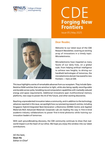
Dear Reader,
Welcome to our latest issue of the CDE Research Newsletter, covering an exciting array of innovations in a timely topic: Microelectronics.
Microelectronics have impacted so many facets of our daily lives, on a global scale. From helping artificial intelligence to achieve new heights, to driving our handheld technologies of tomorrow, the microelectronics domain has soared to new frontiers — here at CDE.
This issue highlights a series of remarkable advances from our ecosystem. They include OptoResistive RAM switches that are sensitive to light, while also being rapidly reconfigurable and durable across cycles, heralding neural computation capabilities with markedly reduced energy and space requirements. Additional innovations span multifunctional memory platforms, new ways to power the AI of the future, and other exciting discoveries.
Reaching unprecedented innovation takes a community, and in addition to the technology advances reported in this issue, we spotlight how our pioneering research centres, including Singapore Hybrid-Integrated Next-Generation u-Electronics (SHINE) Centre and Applied Materials-NUS Advanced Materials Corporate Lab are leading the way in first-in-kind academic-industry collaborations to power first-in-kind photonics while training our innovation leaders of tomorrow.
With each groundbreaking discovery, the CDE community continues to show that realworld impact is at the heart of our ethos. We hope you enjoy this window into our latest contributions.
All the best,
Dean Ho Editor-in-Chief
The quest for Singapore’s technological future

In an era defined by rapid technological change, forwardlooking research and strategic talent development are key to maintaining Singapore’s global leadership in semiconductor innovation. Electrical and
If you’re using the latest smartphones or laptops, you’re experiencing innovations that are, in part, the brainchild of Professor Yeo Yee Chia. Currently serving as the Deputy Chief Executive (Innovation & Enterprise) at the Agency for Science, Technology and Research (A*STAR), and holding a joint appointment at the College of Design and Engineering, National University of Singapore, Prof Yeo’s semiconductor breakthroughs have quietly revolutionised
Issue 05 | May 2025
the devices and services we depend upon every day, from consumer electronics products to the massive data centres that crunch artificial-intelligence workloads.
Bridging research and reality
Forging New Frontiers

Prof Yeo’s semiconductor inventions, comprising more than 330 US patents, describe structures and methods for making transistors with improved speed performance, lower power consumption, and at higher densities or smaller dimensions. These advancements enable the fabrication of chips with increased functionality and reduced energy consumption. One of his contributions is the significant improvement of chip performance through incorporating novel materials in transistors, such as those that enable charge carriers to move at faster speeds. Some of these research ideas were conceptualised by Prof Yeo and his team while at NUS. Breakthroughs were reported by NUS at top technical conferences, and fostered many close collaborations with the industry. Prof Yeo then moved to the industry to implement the most promising ideas.
For eight years, Prof Yeo worked at the forefront of semiconductor innovation at TSMC, a leading semiconductor manufacturing company, developing the world’s most powerful and energy-efficient semiconductor technologies — chips down to three nanometres. The technologies developed have reshaped the landscape of electronics, advancing computing, mobile technology and artificial intelligence at breakneck speeds.
Recently, Prof Yeo has turned his focus back home, driven by a commitment to shape Singapore’s semiconductor research and development (R&D) to contribute to economic impact.
The world is experiencing a major technological upheaval like never before. With a combination of deep industry expertise and a sharp vision for translating research into tangible innovation, Prof Yeo is leading the charge in positioning Singapore as an influential leader in the evolving global semiconductor stage.
Through active management of large-scale national programmes and partnerships with many ecosystem stakeholders, semiconductor R&D efforts in Singapore are now very tightly coordinated, demand-driven, and outcomes-based to deliver economic impact.
Professor Yeo Yee-Chia is leading the charge in positioning Singapore as an influential leader in the evolving global semiconductor stage.
Issue 05 | May 2025
Today at CDE and A*STAR, Prof Yeo translates rigorous scientific inquiry into tangible solutions. His research team recently developed a novel co-packaged optics solution that directly embeds optical components into semiconductor chips for data transfer, which significantly cuts power consumption in data centres.
Balancing Singapore’s position on an increasingly tense geopolitical tightrope between global superpowers is one of Prof Yeo’s strategic contributions. As semiconductor supply chains become progressively fragmented, Singapore’s R&D directions must pivot carefully to maintain relevance. Prof Yeo implements a focused approach, prioritising advanced chip packaging and silicon photonics — fields in which Singapore can lead.
Building the talent pipeline for tomorrow
Prof Yeo’s vision is as much about cultivating talent as it is about developing technology. Throughout his career he has trained a strong, capable workforce as he mentored over 40 doctoral students who now occupy influential roles in academia and industry. Among those mentored by Prof Yeo is Associate Professor Gong Xiao, also from the Department of Electrical and Computer Engineering at CDE, whose research spans advanced transistors, emerging memory technologies and their applications in quantum computing and ultra-high frequency devices.
Above all, Prof Yeo believes that Singapore’s future as a semiconductor powerhouse hinges on continually replenishing its talent pool. He actively shapes initiatives designed to attract international expertise while rigorously training local talent. He prioritises industry-relevant skills and a culture of continuous innovation to set a robust foundation for Singapore’s ongoing leadership in semiconductor research.
“Semiconductor technology is advancing rapidly; if you fail to keep up, you’ll fall behind. And if Singapore doesn’t keep up, the world won’t need us anymore.”
Looking forward, Prof Yeo’s perspective captures the urgency of his role as both scientist and industry leader: “Semiconductor technology is advancing rapidly; if you fail to keep up, you’ll fall behind. And if Singapore doesn’t keep up, the world won’t need us anymore.”
Lighting the path to faster, smarter AI

Bringing non-linearity into the light, a new photonic accelerator allows AI to compute and respond entirely in the optical domain.
As the world thirsts for faster, ever more efficient artificial intelligence (AI), the limits of silicon are beginning to rear their heads. Power-ravenous processors. Clogged interconnects. Algorithms that outpace the hardware meant to run them. It’s a bottleneck that’s hard to ignore — one that puts a cap on tech giants, and one that researchers are racing to break through.
Issue 05 | May 2025 Forging New Frontiers

Professor Aaron Thean led a team to develop a reconfigurable, light-responsive solution that brings true nonlinearity into the photonic fold.
Light may offer the way forward. Photonic computing, where data is processed using light rather than the usual electrons, promises blistering speed, minimal energy loss and vast computing parallelism. In fact, integrated photonics can already perform key AI tasks like matrix multiplications with astonishing efficiency.
But there is a missing piece of the puzzle. One that has kept photonic neural networks from stepping fully into the spotlight.
Without a way to mimic the non-linearity of the brain — how biological neurons respond to signals in nuanced, varied ways — photonic systems remain in the dark. They can add and multiply, but they cannot decide. Processing is possible, but interpreting information is a no-go. And that crucial function, it turns out, has been incredibly challenging to implement.
Research led by Professor Aaron Thean from the Department of Electrical and Computer Engineering, College of Design and Engineering (CDE), National University of Singapore, has shone a light on the path forward, introducing a reconfigurable, light-responsive solution that brings true non-linearity into the photonic fold.
Breaking the linear trap
In a typical artificial neural network, two elements work in tandem. First, weighted sums are computed — multiplying inputs by adjustable values and summing the results. Then comes the non-linear activation function, which introduces flexibility and complexity to model the messiness of the real world, where relationships rarely follow straight lines. It’s this non-linear step, which determines how strongly a neuron should respond, that transforms a simple model into one capable of learning.
“Photonic neural networks have the first part down,” says Prof Thean. “Integrated devices like Mach–Zehnder Interferometer (MZI) meshes can perform the weighted matrix multiplications at blistering speeds, using light as the medium. But introducing non-linearity — in situ, without converting optical signals back into electrical form — has been a long-standing challenge.”
Issue 05 | May 2025
Existing approaches have made some headway. Some incorporate lasers or photodetectors with built-in non-linear behaviours, but these tend to be bulky, power-hungry or limited to fixed responses that can’t adapt from task to task.
Forging New Frontiers
“By embedding these ORS switches into a hybrid structure alongside MZIs and low-power control units, we created a reconfigurable nonlinear activation accelerator.”
The CDE researchers approached the problem from a different angle. Instead of forcing existing devices to bend to non-linear rules, they designed a new kind of component: a light-sensitive Opto-Resistive RAM (ORS) Switch built from solution-processed molybdenum disulfide. This two-dimensional material responds to incoming light by abruptly changing its electrical resistance, a behaviour that can be precisely tuned and repeated over many cycles. They published their findings in the journal Light: Science & Applications
“By embedding these ORS switches into a hybrid structure alongside MZIs and lowpower control units, we created a reconfigurable non-linear activation accelerator,” explains Prof Thean. “It takes in optical signals, converts them into a voltage-driven non-linear response and feeds that signal back into the photonic circuit — completing the neural computation loop without ever leaving the optical domain.”
When tested in simulation on a standard image recognition task using the MNIST handwritten digit dataset, the system delivered a classification accuracy of 91.6%, matching performance benchmarks, while using 20 times less energy and occupying 40% less space than previous photonic architectures.
Towards smarter light
One of the key advantages of the ORS-based accelerator is its reconfigurability. Unlike other non-linear optical elements that are hardwired to one behaviour, the researchers’ system can be programmed to replicate different activation functions, such as ReLU, sigmoid or softplus, depending on the task at hand. This adaptability lays the groundwork for a broader class of AI models running efficiently on light-based platforms.
The team’s compact, energy-efficient design also makes photonic AI hardware practical for real-world deployment, especially in applications where speed and power budgets are critical: autonomous systems, real-time data processing or edge AI devices.
Looking ahead, the team aims to integrate lithium niobate photonic components with the silicon photonics platform, combining the maturity and high performance of silicon photonics technology with the enhanced functionality of lithium niobate. This integration is essential for enabling the next generation of advanced AI applications.
You heard it here first: AI, at the speed of light! Issue 05 | May 2025
Research Centre
Shining a light on chip chatter

From lab concept to real-world integration, a multiinstitutional collaboration produces a compact photonic modulator-memory device that turbocharges how data moves between computer chips — more efficiently, with far less energy.
As the world’s voracious appetite for data grows ever larger, so too does the need for microelectronic systems to keep up. From data centres to AI processors to edge computing to next-generation communications, tomorrow’s technologies will need faster, more efficient ways for chips to talk to each other.
Issue 05 | May 2025
Hosted at the College of Design and Engineering, the Singapore Hybrid-Integrated Next-Generation μ-Electronics (SHINE) Centre is leading efforts to meet this challenge. At the intersection of materials science, electronics and photonics, the Centre brings together researchers across disciplines to develop advanced microelectronics with an emphasis on real-world impact. As a platform for academic-industry collaboration, SHINE also offers opportunities for partners across the semiconductor value chain to co-develop and translate emerging technologies into practical applications.
Researchers at SHINE recently demonstrated, for the first time, a compact device that unifies optical modulation and memory. This paves the way for a faster, more energy-efficient and adaptable way for microchips to communicate, one that could bring data-processing to new frontiers.
Forging New Frontiers
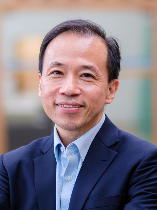
Professor
the
brings together researchers across disciplines to develop advanced microelectronics with an emphasis on real-world impact.
The collaborative project brought together a multidisciplinary team from SHINE; the Integrative Sciences and Engineering Program, NUS Graduate School; the School of Electronics and Information Technology, Sun Yat-Sen University, China; the Centre for Quantum Technologies, NUS; and industry partner POET Technologies.
The team’s paper was selected for the IEEE International Electron Devices Meeting that took place from 9–13 December 2023 in San Francisco.
Untangling the gridlock
To speed up chip-to-chip communication, researchers are increasingly turning away from traditional electrical connections and turning to photonics, where beams of light ferry information instead of electrons. Because photons don’t face electrical resistance, they move swiftly and cleanly. This means faster data flows, using less energy, without generating excessive heat.
But translating this potential into real-world applications hasn’t been an easy cruise. One major roadblock has been the lack of devices capable of modulating and storing optical signals concurrently. Existing modulators, which convert electrical signals to optical ones, tend to be power-hungry and lack built-
Aaron Thean directs
SHINE Centre, which
Issue 05 | May 2025 Forging New Frontiers
“The ferroelectric properties of HZO create stable electric fields that influence the optical properties of LNOI.”
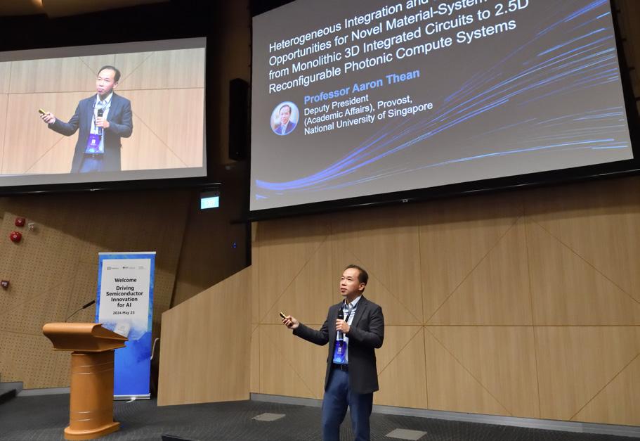
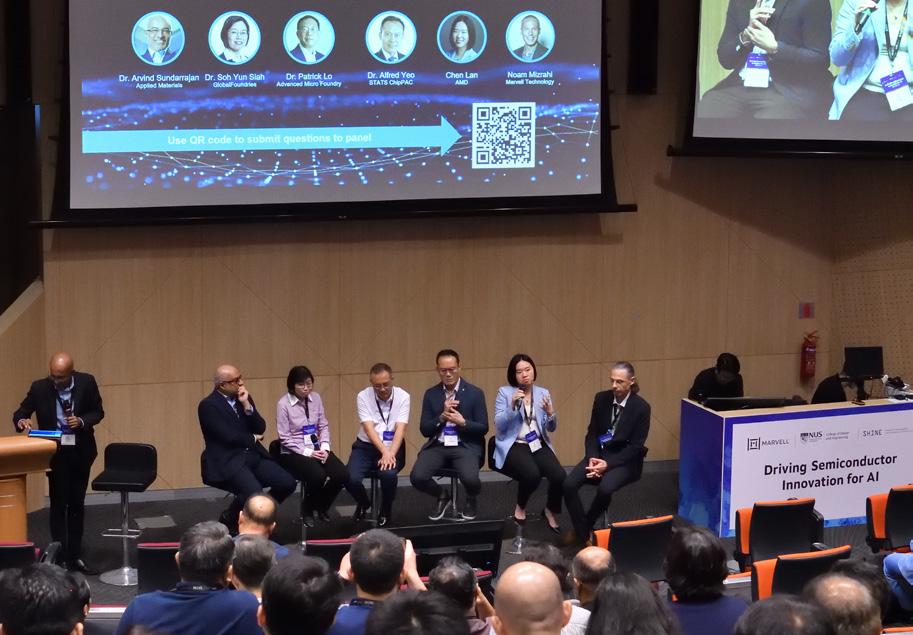
(Top) Keynote speaker Professor Aaron Thean, Deputy President (Academic Affairs) and Provost of NUS, outlined ways CDE and SHINE Centre have been expanding the talent pool in the semiconductor industry.
(Bottom) The panel from left to right: Dr Radha Nagarajan (Marvell Technology), Dr Arvind Sundarrajan (Applied Materials), Dr Siah Soh Yun (GlobalFoundries), Dr Patrick Lo (Advance Micro Foundry), Dr Alfred Yeo (STATS ChipPAC), Ms Chen Lan (AMD) and Mr Noam Mizarhi (Marvell Technology).
in memory. Without memory, these systems must constantly refresh their settings, which undermine efficiency and flexibility.
Tackling this challenge head-on, the collaborative team designed a compact electro-optic modulator with integrated memory — a device they dubbed ElectroOptic Modulator and Memory (EOMM). They achieved this by combining lithium niobate on insulator (LNOI), a material known for its ability to alter how light behaves under an electric field, with hafnium zirconium oxide (HZO), a ferroelectric material that retains memory states without the need for continuous power.
“The ferroelectric properties of HZO create stable electric fields that influence the optical properties of LNOI. This imprints memory states onto the device,” explains Professor Aaron Thean, Director of the SHINE Centre. “Unlike conventional modulators, this design doesn’t need constant electrical input to remember its configuration, significantly cutting down energy usage and enhancing operational efficiency.”
To further enhance the performance of the EOMM, the team incorporated indium-tin oxide electrodes, which allow light to be controlled electrically without blocking it, keeping signals clean and sharp. They also integrated tiny resistive heaters to provide an additional way to fine-tune the light when needed. Together, these features give the device both speed and flexibility.
Real-world potential
Working with industry partner POET Technologies, a developer of advanced photonic integration platforms, the researchers took their innovation one step closer to real-world deployment. They integrated the EOMM device into POET Technologies’ high-speed optical interposer chip (400G Tx/Rx) to test how the technology could perform in a commercial-grade photonic system.
In simulated models of chiplet-tochiplet communication networks, where multiple chips communicate through a shared photonic interconnect, the EOMM-enabled system achieved up to 70% power savings compared to conventional electrical links, and 30–50% lower energy consumption compared to optical systems that still rely on electronic routing.

“Through cross-disciplinary collaboration and close partnerships with industry, research like this highlights the realworld potential for commercial reconfigurable photonic systems that can adapt on the fly,” adds Prof Thean. “Enabling memory and modulation in a single device is a holy grail for faster, smarter and more efficient chip communication in high-performance environments like data centres, AI processors and photonic neural networks.”
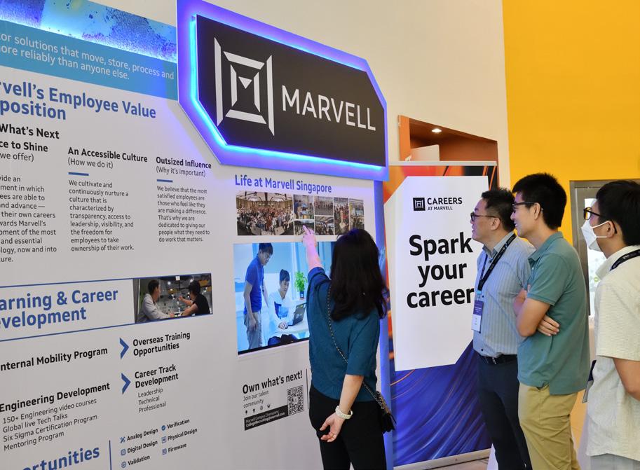
(Top) Participants looking at the career opportunities and programmes available at Marvell.
(Bottom) Participants engage with informative posters at the forum, exploring the work Marvell does and potential opportunities.
Where atoms are engineered into impact

Forging new frontiers in semiconductor materials, the AMAT–NUS Advanced Materials Corporate Lab enters a new phase featuring advanced facilities, deeper industry integration and a strong focus on talent development.
t’s easy to overlook the tiny architectures that make modern life tick. The chips inside your smartphone. The motherboards that your car relies on. The servers crunching data behind every search and swipe.
Issue 05 | May 2025

Our modern society depends on the rapid and affordable scaling of computing performance in nearly every aspect of daily life, from consumer electronics to communications to national security. But traditional materials and manufacturing methods are nearing their limits. With the increasing demands of artificial intelligence, machine learning and the Internet-ofThings, a paradigm shift is needed. That shift will be driven by the development of novel materials and innovative processing strategies — efforts that require close collaboration between industry and academia. This is particularly crucial for Singapore, where electronics constitute more than 9% of the national GDP and serve as a critical pillar of the economy.
Bridging that gap is the Applied Materials–NUS Advanced Materials Corporate Lab, hosted at the College of Design and Engineering (CDE) and the Faculty of Science at NUS. Since its establishment in 2018, the Lab, a collaboration between NUS and Applied Materials Inc. (AMAT), has grown into a global leader in semiconductor innovation. It aligns with Singapore’s broader national goals under the Research, Innovation and Enterprise 2025 (RIE2025) plan and Applied Materials’ “Singapore 2030” plan to strengthen its manufacturing capacity, R&D capabilities, technology ecosystem partnerships and workforce development in the city-state.
The Lab is underpinned by a unique, hybrid model that blends academia’s curiosity-driven inquiry with the customer-focused rigour of industry R&D. This is driven by a “try-fast-fail-fast” approach that enables rapid feedback and iteration between researchers and engineers. Over the past six years, this ecosystem has delivered more than 70 patent filings and technology disclosures and the successful transition of multiple low-TRL projects to industry-relevant technologies.
In the first phase, the Lab focused on application-inspired, fundamental materials research — designing and demonstrating new processes, and building a scientific understanding from first principles. “We have achieved promising results in Phase 1. In particular, we have transferred four high-value projects to the scaleup phase in Applied Materials,” says Professor Silvija Gradecak-Garaj from the Department of Materials Science and Engineering at CDE, and Co-Director of the Lab.
Professor Silvija Gradecak-Garaj is one of the Co-Directors of the Applied Materials–NUS Advanced Materials Corporate Lab, hosted at CDE.
Issue 05 | May 2025
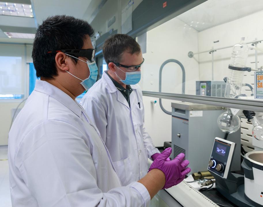
Working as a multi-disciplinary team, the Applied MaterialsNUS Advanced Materials Corporate Lab researchers combine theoretical and experimental approaches, as well as engineering and scientific expertise, to develop new materials critical for the semiconductor industry.
At the heart of these achievements are the Lab’s innovations in materials engineering for next-generation semiconductor technologies. “One high-value project addressed the future challenges of stacking memory devices, in which engineers from AMAT and NUS have developed novel processes that tackle key technology inflection points in memory density scaling,” says Dr John Sudijono, Director of Engineering at AMAT and Co-Director of the Lab. The project developed nanostructured diamond films — an enabling technology for advanced semiconductor architectures such as 3D NAND and DRAM.
The Lab has also broken new ground in two-dimensional materials, pioneering a method for wafer-scale growth at back-end-of-line (BEOL) compatible temperatures, with applications in microelectronic interconnects and logic components, and has already attracted interest from major industry players.
These outcomes, says Prof Gradecak-Garaj, are a result of a multidisciplinary collaboration between AMAT and NUS. “We combine theoretical and experimental approaches, as well as engineering and scientific expertise, to tackle high-value problems of the semiconductor industry.”
Expanding the possibilities
Officially launched by Deputy Prime Minister Heng Swee Keat in October 2024, Phase 2 of the Lab includes a larger, more advanced cleanroom with state-ofthe-art semiconductor process equipment and enhanced R&D capabilities for material synthesis and characterisation.
This next phase continues to focus on developing industry-scale solutions to real-world manufacturing challenges, with an emphasis on integrating multiple processing steps, developed in Phase 1, into a single, optimised flow. “This will not only lower production time and costs, but also enable new materials and processes required for the next-generation electronics that are integral to fields spanning healthcare, automotive, telecommunications and artificial intelligence,” adds Prof Gradecak-Garaj.
Issue 05 | May 2025 Forging New Frontiers
Many of these applications are being tailored to work with Applied Material’s Endura platform, the industry’s most widely adopted cluster tool for depositing thin metal films. The focus on new materials understanding, as well as materials engineering developed in this second phase, will provide enhanced value-add to Applied Materials to meet the performance and power requirements of advanced semiconductors.
Growing talent for the long game
“The Lab is also a training ground for talent. Since its inception, it has supported more than 70 PhD students, researchers and interns, many of whom have gone on to contribute across Singapore’s semiconductor industry,” says Professor Richard Wong from the Department of Chemistry, Faculty of Science, NUS, who is also a Co-Director of the Lab. Phase 2 will deepen that commitment, with new courses, internships and co-developed educational programmes at NUS focused on microelectronics, advanced materials and process engineering.


Phase
and
to right: Mr Brian Tan, Regional President (Southeast Asia), Applied Materials; Dr Satheesh Kuppurao, Group Vice President, Applied Materials; Mr Heng Swee Keat, Deputy Prime Minister and Chairman, National Research Foundation; Mr Hsieh Fu Hua, Chairman, NUS Board of Trustees; and Professor Tan Eng Chye, President, NUS.
(Bottom) Deputy Prime Minister Heng Swee Keat was given a tour of exhibits that showcased cutting-edge solutions and breakthroughs in material science, microelectronics and other areas.
“The centrepiece of this success is the Lab’s collaborative model — one that brings together academia and industry to generate novel ideas and to move them into practice,” adds Prof Gradecak-Garaj. “We look forward to the continued success of Phase 2 as we work towards translating more advanced materials research into impactful solutions.”
(Top)
II of the Applied Materials-NUS Advanced Materials Corporate Lab was launched by Guest-of-Honour Deputy Prime Minister
Chairman of the National Research Foundation, Mr Heng Swee Keat (middle). From left
A smarter way to power artificial intelligence

A fully integrated compute-in-memory system pairs 2D memristors with silicon selectors to offer a practical, energyefficient route for powering next-gen AI applications.
ith a simple click, your hastily taken photo sharpens, a garbled voice message turns into polished text and a chatbot drafts an email in perfect prose. Today’s digital tools, enhanced by artificial intelligence (AI), seem to perform magic on demand.

Associate Professor Ang Kah Wee and his team developed a fully integrated CIM system that stores and processes data in the same physical space.
But behind every interaction lies an unseen cost. Running state-of-the-art AI models is tied to staggering amounts of computing power — and gobbles up massive amounts of energy. Training a large language model like GPT-3, for instance, comes with a price tag upwards of $10 million. You’ll also need more than 700,000 litres of water to do that. Each query or task that follows continues to tap into energy-hungry infrastructure to retrieve, compute and respond.
Part of the problem is the machines themselves. Most computers today are still built around hardware introduced over 75 years ago, and rely on the transistor device first invented in 1947. This arrangement has served generalpurpose computing well for decades, but it creates a data traffic jam for AI, as it separates compute and memory. This means data must constantly shuttle between memory and processor — slamming figurative brakes on workflows while guzzling disproportionate amounts of power.
“AI workloads are memory-centric,” says Associate Professor Ang Kah Wee from the Department of Electrical and Computer Engineering at the College of Design and Engineering, National University of Singapore. “It’s not the computing that takes time or power — it’s all the moving of data.”
Indeed, this bottleneck is becoming increasingly unsustainable as AI enters the vocabulary of everyday people. And amidst this challenge has emerged the concept of “compute-in-memory” (CIM), which harnesses memristors to process and store data all in one place.
Unlike traditional transistors, which rely on the movement of electrons and lose data when powered down, memristors work more like the human brain. They use ions to carry information and can “remember” their resistance state even without power. This allows them to store and process data at the same location — eliminating the need for constant data transfers between separate memory and computing units.
However, making them work at scale, especially with advanced two-dimensional (2D) materials that are all the buzz, has remained an engineering challenge, stymied by control issues, signal interference and limited integration with conventional circuitry.
Issue 05 | May 2025
A new kind of memory machine
Forging New Frontiers
Assoc Prof Ang led a team to develop a fully integrated CIM system that stores and processes data in the same physical space. Detailed in their Nature Communications paper published on 19 March 2025, the system is built around a 32x32 array of memristors made from hafnium diselenide, an ultra-thin 2D material with low energy requirements and rapid switching speeds. A key element of the design is the silicon-based selector that sits beneath each memristor.
“These selectors act like traffic controllers to ensure that only the targeted memristor switches on, while others remain unaffected.”
“These selectors act like traffic controllers to ensure that only the targeted memristor switches on, while others remain unaffected,” explains Assoc Prof Ang. “This averts unwanted electrical interference, known as sneak current, that can corrupt data in large memristor arrays.”
Pairing each memristor with a selector in a one-selector-one-memristor configuration forms a tightly packed, high controllable network. Further, the method used to assemble the device allows the fragile memristor switching layer to be transferred directly onto a silicon substrate without damage — making it compatible with existing semiconductor manufacturing techniques.
The team went on to build a complete working system by integrating peripheral circuitry to manage inputs, outputs and computations. Instead of relying on conventional analog-to-digital converters, which are bulky and power-hungry, they designed time-domain sensing circuits that interpret electrical signals by measuring how long it takes for voltage changes to occur. This approach speeds up data readout and uses less than half the power of traditional methods.
The system also takes advantage of the natural non-linear behaviours of these circuits to implement built-in activation functions — essential components in neural networks that mimic how biological neurons “fire”. When embedded directly into hardware, the activation functions help the system avoid additional processing steps to further improve efficiency.
05 | May 2025
The outcome is a fast, compact and energy-efficient CIM platform. The memristors switch in nanoseconds and can endure more than 26,000 programming cycles without degradation. When tested on a pattern recognition task using a simple convolutional neural network, the system achieved 97.5% accuracy — a level comparable to conventional digital systems, but at a fraction of the energy cost.
From lab to fab
“Being siliconcompatible, our method also doesn’t require clean-sheet manufacturing nor exotic materials.”
Merging memory and processing into one architecture reduces latency and energy demand while increasing throughput — all within a compact device. This approach could be a game-changer for applications where power is limited but performance is critical, such as AI-based edge computing and autonomous systems.
“Being silicon-compatible, our method also doesn’t require clean-sheet manufacturing nor exotic materials,” adds Assoc Prof Ang. “We think it’s very practical for realworld AI hardware.”
The team is exploring ways to expand the array size and handle more complex datasets, with an eye toward real-time deployment. Interestingly, the combination of fast switching, reliable endurance and low-voltage operation makes their system particularly well-suited for neuromorphic computing — hardware that mimics how the brain processes information.
Bridging light and electrons

A new ferroelectric memory device stores and retrieves data using both light and electricity, offering a compact and scalable solution to bridge electronic and photonic computing systems.
Did you know that nearly every microprocessor today — from those in smartphones to supercomputers — still runs on a design architecture conceived in the 1940s?
Issue 05 | May 2025 Forging New Frontiers
Known as the vonn Neumann architecture, it separates memory and processing units and connects them via a shared data channel. While the architecture has underpinned decades of progress, it’s showing its age in the face of increasingly data-intensive technologies such as artificial intelligence. Moving data between memory and processor takes time, wastes energy and hamstrings performance.
Associate Professor Gong Xiao has a solution: a compact, silicon-compatible memory cell that stores data using light or electricity, and reads it in both formats, simultaneously. At the Department of Electrical and Computer Engineering, College of Design and Engineering, National University of Singapore, Assoc Prof Gong led a team to build this photonic-electronic memory using a thin film of ferroelectric material on a silicon ring resonator — a design that retains data without power and operates at telecom wavelengths.
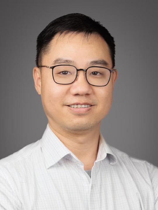
Together with his team, Associate Professor Gong Xiao built a photonic-electronic memory using a thin film of ferroelectric material on a silicon ring resonator.
The stable, low-power and multi-modal memory device could help bridge the gap between photonic and electronic systems. It is also compatible with existing chip manufacturing processes, which makes it easier to scale for real-world applications, from high-speed data centres to processors that mimic the human brain.
The researchers’ findings were published in Light: Science & Applications on 23 August 2024.
Overcoming the memory bottleneck
Photonic microchips, which process data using light instead of electricity, offer faster speeds and lower power usage. However, many photonic devices lack a simple and efficient way to store information directly as light. Each time data must be saved, light signals are converted back into electrical ones, and then converted back to light for processing. This back-and-forth adds delays and chips away at the benefits of photonic computing.
To realise the potential of photonics, researchers have been searching for a memory device that can store data using both electrical and optical inputs, and outputs data in either form. It would also need to retain information even when the power is off — a feature known as non-volatility.
Issue 05 | May 2025
While various solutions such as the use of materials like phase-change films have shown some promise, they tend to introduce instability, complexity in programming or incompatibility with the standard silicon processes that underpin modern computing.
Assoc Prof Gong’s team took a fresh approach. They designed a memory cell around a silicon ring resonator, a tiny structure through which light circulates continuously. Onto this resonator, the team applied an ultra-thin layer of aluminium-doped hafnium oxide — a ferroelectric material that responds to small electrical changes by shifting the orientation of its internal electric dipoles.
“Ferroelectric materials let us control a kind of built-in polarity.”
“Ferroelectric materials let us control a kind of built-in polarity,” explains Assoc Prof Gong. “Once set by a voltage or even light, that state holds, and we don’t need to keep using power to maintain the data.”
This change in polarity affects two things at once: it alters the capacitance (how the device responds electrically) and the refractive index (how it interacts with light). As a result, the same memory cell can be written and erased using either electrical pulses or light, and read through both electrical sensing and optical signals — with no interference between the two.
By varying the strength of the input signals, the team was also able to store multiple levels of data in a single cell — not just simple ones and zeroes, but multiple states such as 00, 01, 10 and 11. This means more storage in a smaller footprint and less overall energy use per bit. Further tests showed that the memory was stable, energy-efficient and reliable across many repeated uses. It also retained data for long periods and required only low voltages to operate.
Towards unified computing systems
Acting as a bridge between photonic and electronic systems, the team’s invention could enable faster, more efficient platforms for data centres, optical interconnects and neuromorphic processors that mimic how the brain processes information.
In addition, because the design is CMOS-compatible, it can be integrated into existing chip manufacturing processes and scaled to dense memory arrays. The
05 | May 2025
team is currently focused on enhancing switching speed, reducing power consumption and integrating additional components directly on-chip to improve overall system efficiency. In parallel, they are pushing toward a large-scale demonstration of photonic computing tightly integrated with electronic systems. This hybrid approach aims to leverage the scalability and versatility of heterogeneous integration, paving the way for high-performance, energyefficient computing platforms suitable for next-generation data processing and AI workloads.
Capacitive memory gets a charge
While ferroelectric materials have opened new vistas in photonic-electronic memory, their potential stretches far beyond. In a recent review, Assoc Prof Gong takes a bird’s-eye view of how ferroelectric capacitive memories (FCMs) could shape the future of data storage and energyefficient computing.
Published in Nano Convergence on 22 January 2025, the review explores how these emerging memory devices store data not by switching resistive states, but by altering capacitance — a charge-based method that enables non-destructive readout, ultra-low power consumption and better scalability in chip arrays.
Unlike conventional resistive memories, FCMs offer unique advantages in largescale systems: they sidestep common pitfalls like voltage loss and “sneak path” errors, which often plague dense memory networks. The review also highlights how FCMs could accelerate computingin-memory for machine learning — performing computations within memory cells to reduce data transfer overhead.
A chip off the old block

A single transistor can mimic the neural and synaptic behaviours of the human brain, bringing biologically inspired computing closer to reality.
The human brain is a remarkable computing machine. The IBM Summit supercomputer, once the world’s fastest supercomputer, can perform 200 quadrillion (that’s 15 zeros) calculations per second, using around 15 megawatts, enough to power thousands of homes. By comparison, the human brain, weighing just over a kilogram, achieves more than five times the
Issue 05 | May 2025
computational capacity, all while consuming less energy than a household lightbulb.
Mind-blowing stuff. It’s little wonder, then, that scientists are so keen to replicate the performance of the human brain.
Researchers led by Associate Professor Mario Lanza from the Department of Materials Science and Engineering, College of Design and Engineering (CDE), National University of Singapore (NUS), have demonstrated that a single, standard silicon transistor, the fundamental building block of microchips used in computers, smartphones and almost every electronic system, can function like a biological neuron and synapse when operated in a specific, unconventional way.

The research team’s work presents a highly scalable and energy-efficient solution for hardware-based artificial neural networks (ANNs). This brings neuromorphic computing — where chips could process information more efficiently, much like the human brain — closer to reality. Their study was published in the journal Nature on 26 March 2025.
Putting the brains in silicon
The world’s most sophisticated computers already exist inside our heads. Studies show that the human brain is, by and large, more energy-efficient than electronic processors, thanks to almost 90 billion neurons that form some 100 trillion connections with each other, and synapses that tune their strength over time — a process known as synaptic plasticity, which underpins learning and memory.
For decades, scientists have sought to replicate this efficiency using ANNs. ANNs have recently driven remarkable advances in artificial intelligence (AI), loosely inspired by how the brain processes information. But while they borrow biological terminology, the similarities run only skin deep — software-based ANNs, such as those powering large language models like ChatGPT, have a voracious appetite for computational resources and, hence, electricity. This makes them impractical for many applications.
Associate Professor Mario Lanza and his team demonstrated that a standard silicon transistor can function like a biological neuron and synapse.
Issue 05 | May 2025
Forging New Frontiers
Neuromorphic computing aims to mimic the computing power and energy efficiency of the brain. This requires not only re-designing system architecture to carry out memory and computation at the same place — called in-memory computing — but also the development of electronic devices that exploit physical and electronic phenomena capable of replicating how neurons and synapses work. However, current neuromorphic computing systems are stymied by the need for complicated multi-transistor circuits or emerging materials that are yet to be validated for large-scale manufacturing.
“To enable true neuromorphic computing, where microchips behave like biological neurons and synapses, we need hardware that is both scalable and energyefficient,” said Assoc Prof Lanza.
“To enable true neuromorphic computing, where microchips behave like biological neurons and synapses, we need hardware that is both scalable and energyefficient.”
The researchers have now demonstrated that a single, standard silicon transistor, when arranged and operated in a specific way, can replicate both neural firing and synaptic weight changes — the core mechanisms of biological neurons and synapses. This was achieved through adjusting the resistance at the transistor’s bulk terminal, which in turn allowed the team to control two key physical phenomena within the device: impact ionisation, which generates a current spike akin to the activation of an electronic neuron, and charge trapping, which causes the resistance state to persist over time, mimicking the long-term behaviour of a synapse. Building on this, the team designed a two-transistor cell, called Neuro-Synaptic Random Access Memory (NS-RAM), that can switch between neuron and synapse modes dynamically.
“Other approaches require complex transistor arrays or novel materials with uncertain manufacturability, but our method makes use of commercial CMOS (complementary metal-oxide-semiconductor) technology, the same platform found in modern computer processors and memory microchips,” explained Assoc Prof Lanza. “This means it’s scalable, reliable and compatible with existing semiconductor fabrication processes.”
Issue 05 | May 2025
Through experiments, the NS-RAM cell demonstrated low power consumption, maintained stable performance over many cycles of operation and exhibited consistent, predictable behaviour across different devices — all of which are desired attributes for building reliable ANN hardware suited for real-world applications. The team’s breakthrough marks a step change in the development of compact, power-efficient AI processors that could enable faster, more responsive computing.
“The transistors we used are not at the cutting-edge — but rather traditional 180-nanometre node transistors, which can be produced by Singapore-based companies,” adds Assoc Prof Lanza. “Now that we’ve understood the operating mechanism, it’s now more a matter of microelectronic design.”
Forging New Frontiers
Memristors for fast and energy-efficient AI
In another paper, also published in Nature on 16 April 2025, Assoc Prof Lanza and his team dissected how the memristor industry is advancing, and how it is going to affect our lives.
Memristive circuits offer a major advantage for AI hardware as they enable data to be stored and processed simultaneously. This reduces energy consumption and latency, making them more efficient than conventional architectures that separate memory and processing units. From the current state of transistor-based memory, to the rise of memristors, as well as their scalability challenges and the central role of collaboration between academia, startups and chip manufacturers, the researchers offered expert analysis and forward-looking insights into this emerging technology in their comprehensive review.
“The development of memristive materials and devices has been extensively studied for more than 15 years, and now it is time to start to focus on hybrid memristortransistor implementations that result in realistic products,” says Assoc Prof Lanza. “We are now working on a multidisciplinary project to bring 2D memristors into reality, joining efforts from materials science, physics, chemistry, electrical engineering and even AI.”
