ON PROGNOZISYS OF MANUFACTURING DOUBLE-BASE
HETEROTRANSISTOR AND OPTIMIZATION OF TECHNOLOGICAL PROCESS
E.L. Pankratov1,3, E.A. Bulaeva1,2
2
1
Nizhny Novgorod State University, 23 Gagarin avenue, Nizhny Novgorod, 603950, Russia
Nizhny Novgorod State University of Architecture and Civil Engineering, 65 Il'insky street, Nizhny Novgorod, 603950, Russia
3
Nizhny Novgorod Academy of the Ministry of Internal Affairs of Russia, 3 Ankudinovskoe Shosse, Nizhny Novgorod, 603950, Russia
ABSTRACT
In this paper we introduce a modification of recently introduced analytical approach to model mass- and heat transport. The approach gives us possibility to model the transport in multilayer structures with account nonlinearity of the process and time-varing coefficients and without matching the solutions at the interfaces of the multilayer structures. As an example of using of the approach we consider technological process to manufacture more compact double base heterobipolar transistor. The technological approach based on manufacturing a heterostructure with required configuration, doping of required areas of this heterostructure by diffusion or ion implantation and optimal annealing of dopant and/or radiation defects. The approach gives us possibility to manufacture p n- junctions with higher sharpness framework the transistor. In this situation we have a possibility to obtain smaller switching time of p n- junctions and higher compactness of the considered bipolar transistor.
KEYWORDS
Double-base heterotransistors, increasing of integration rate of transistors, analytical approach to model technological processes
1. INTRODUCTION
In the present time performance and integration degree of elements of integrated circuits intensively increasing (p n-junctions, field-effect and bipolar transistors, ...) [1-6]. To increase the performance it could be used materials with higher values of speed of transport of charge carriers, are developing new and optimization of existing technological processes [7-10]. To increase integration degree of elements of integra-ted circuits (i.e. to decrease dimensions of elements of integrated circuits) are developing new and optimization of existing technological processes. In this case it is attracted an interest laser and microwave types of annealing of dopant and/or radiation defects [11-13], inhomogeneity (existing of several layers) of heterostructures [14-17], radiation processing of doped materials [18].
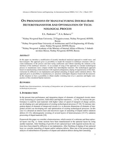
Framework this paper we consider a heterostructure, which consist of a substrate and three epitaxial layers (see Fig. 1). Some sections have been manufactured in the epitaxial layers by using another materials. After finishing of growth of new epitaxial layer with required sections the sections have been doped by diffusion or ion implantation. After finishing of doping of last epitaxial layer we consider annealing of dopant and/or radiation defects. Main aim of the present paper is analysis of redistribution of dynamics of dopant and radiation defects during their annealing.
Advances in Materials Science and Engineering: An International Journal (MSEJ), Vol. 2, No. 1, March 2015
Fig. 1. Heterostructure with a substrate with three epitaxial layers and sections in the layers
2. Method of solution
To solve our aim we determine spatio-temporal distribution of concentration of dopant. We determine the distribution by solving the second Ficks law in the following form [1,14,16-18] ( ) ( ) ( ) ( ) + + = z tzyx C D z y tzyx C D y x tzyx C D x t tzyx C C C C ∂ ∂ ∂ ∂ ∂ ∂ ∂ ∂ ∂ ∂ ∂ ∂ ∂ ∂ ,,, ,,, ,,, ,,, (1)
with boundary and initial conditions ( ) 0 ,,, 0
= ∂ ∂ =x x tzyx C , ( ) 0 ,,, = ∂ ∂ = x Lx x tzyx C , ( ) 0 ,,, 0
= ∂ ∂ = z z tzyx C , ( ) 0 ,,, = ∂ ∂ = z Lx z tzyx C , C (x,y,z,0)=f (x,y,z).
= ∂ ∂ = y y tzyx C , ( ) 0 ,,, = ∂ ∂ = y Lx y tzyx C , (2) ( ) 0 ,,, 0
Here C(x,y,z,t) is the spatio-temporal distribution of concentration of dopant; T is the temperature of annealing; DС is the dopant diffusion coefficient. Value of dopant diffusion coefficient depends on properties of materials, speed of heating and cooling of heterostructure (with account Arrhenius law). Dependences of dopant diffusion coefficients could be approximated by the following function [19-21] () ( ) () ( ) ( ) () + + + = 2 *
2 2 * 1 ,,, ,,, 1 ,,, ,,, 1 ,,, V tzyx V V tzyx V Tzyx P tzyx C Tzyx D D L C ς
where DL(x,y,z,T) is the spatial (due to existing several layers wit different properties in heterostructure) and temperature (due to Arrhenius law) dependences of dopant diffusion coefficient; P (x,y,z,T) is the limit of solubility of dopant; parameter γ could be integer framework the following interval γ∈[1,3] [19]; V (x,y,z,t) is the spatio- temporal distribution of concentration of radiation vacancies; V * is the equilibrium distribution of concentration of vacancies. Concentrational dependence of dopant diffusion coefficient have been discussed in details in [19]. It should be noted, that using diffusion type of doping did not leads to generation radiation defects and ζ1= ζ2= 0. We determine spatio-temporal distributions of concentrations of point defects have been determine by solving the following system of equations [20,21]
Advances in Materials Science and Engineering: An International Journal (MSEJ), Vol. 2, No. 1, March 2015
( ) () ( ) () ( ) + ∂ ∂ ∂ ∂ + ∂ ∂ ∂ ∂ = ∂ ∂ y tzyxI Tzyx D y x tzyxI Tzyx D x t tzyxI I I ,,, ,,, ,,, ,,, ,,, () ( ) ()()()()() tzyx ITzyx k tzyxVtzyxITzyx k z tzyxI Tzyx D z II VI I ,,, ,,, ,,, ,,, ,,, ,,, ,,, 2 , , ∂ ∂ ∂ ∂ + ( ) () ( ) () ( ) + ∂ ∂ ∂ ∂ + ∂ ∂ ∂ ∂ = ∂ ∂ y tzyx V Tzyx D y x tzyx V Tzyx D x t tzyx V V V ,,, ,,, ,,, ,,, ,,, (4) () ( ) ()()()()() tzyx V Tzyx k tzyxVtzyxITzyx k z tzyx V Tzyx D z VV VI V ,,, ,,, ,,, ,,, ,,, ,,, ,,, 2 , , ∂ ∂ ∂ ∂ + with boundary and initial conditions ( ) 0 ,,, 0
= ∂ ∂ =x x tzyx ρ , ( ) 0 ,,, = ∂ ∂ = x Lx x tzyx ρ , ( ) 0 ,,, 0
= ∂ ∂ =y y tzyx ρ , ( ) 0 ,,, = ∂ ∂ = y Ly y tzyx ρ , ( ) 0 ,,, 0
= ∂ ∂ = z z tzyx ρ , ( ) 0 ,,, = ∂ ∂ = z Lz z tzyx ρ , ρ(x,y,z,0)=fρ(x,y,z). (5)
Here ρ=I,V; I(x,y,z,t) is the spatio-temporal distribution of concentration of radiation interstitials; Dρ(x,y,z,T) is the diffusion coefficients of radiation interstitials and vacancies; terms V2(x, y,z,t) and I2(x,y,z,t) correspond to generation of divacancies and diinterstitials; kI,V(x,y,z,T) is the parameter of recombination of point radiation defects; kρ,ρ(x,y,z,T) are the parameters of generation of simplest complexes of point radiation defects.
We determine spatio-temporal distributions of concentrations of divacancies ΦV(x,y,z,t) and diinterstitials Φ I (x,y,z,t) by solving the following system of equations [20,21] ( ) () ( ) () ( ) + Φ + Φ = Φ Φ Φ y tzyx Tzyx D y x tzyx Tzyx D x t tzyx I I I I I ∂ ∂ ∂ ∂ ∂ ∂ ∂ ∂ ∂ ∂ ,,, ,,, ,,, ,,, ,,, () ( ) ()()()() tzyxITzyxk tzyx ITzyx k z tzyx Tzyx D z I II I I ,,, ,,, ,,, ,,, ,,, ,,, 2 , + Φ + Φ ∂ ∂ ∂ ∂ (6) ( ) () ( ) () ( ) + Φ + Φ = Φ Φ Φ y tzyx Tzyx D y x tzyx Tzyx D x t tzyx V V V V V ∂ ∂ ∂ ∂ ∂ ∂ ∂ ∂ ∂ ∂ ,,, ,,, ,,, ,,, ,,, () ( ) ()()()() tzyx VTzyx k tzyx VTzyx k z tzyx Tzyx D z V VV V V ,,, ,,, ,,, ,,, ,,, ,,, 2 + Φ + Φ ∂ ∂ ∂ ∂ with boundary and initial conditions ( ) 0 ,,, 0
= ∂ Φ∂ = y y tzyx ρ , ( ) 0 ,,, = ∂ Φ∂ = y Ly y tzyx ρ , ( ) 0 ,,, 0
= ∂ Φ∂ =x x tzyx ρ , ( ) 0 ,,, = ∂ Φ∂ = x Lx x tzyx ρ , ( ) 0 ,,, 0
= ∂ Φ∂ = z z tzyx ρ , ( ) 0 ,,, = ∂ Φ∂ = z Lz z tzyx ρ , (7) Φ I (x,y,z,0)=fΦI(x,y,z), ΦV(x,y,z,0)=fΦV(x,y,z).
Advances in Materials Science and Engineering: An International Journal (MSEJ), Vol. 2, No. 1, March 2015
Here DΦρ(x,y,z,T) are the diffusion coefficients of complexes of radiation defects; kρ(x,y,z,T) are the parameters of decay of complexes of radiation defects.
We determine spatio-temporal distributions of concentrations of dopant and radiation defects by using method of averaging of function corrections [22] with decreased quantity of iteration steps [23]. Framework the approach we used solutions of Eqs. (1), (4) and (6) in linear form and with averaged values of diffusion coefficients D0L, D0I, D0V, D0ΦI, D0ΦV as initial-order approximations of the required concentrations. The solutions could be written as () ()()()() ∑ + = ∞ =1
0 1 2 ,,, n nC n n nnC zyx zyx
C t cxezcy c F LLL LLL F tzyx C , () ()()()() ∑ + = ∞ =1
0 1 2 ,,, n nI n n nnI zyx zyx
I t cxezcy cF LLL LLL F tzyxI , () ()()()() ∑ + = ∞ =1
0 1 2 ,,, n nV n n nnC zyx zyx
C t cxezcy c F LLL LLL F tzyx V , () ()()()() ∑ + = Φ ∞ Φ Φ Φ 1
0 1 2 ,,, n n n n n n zyx zyx I t cxezcy c F LLL LLL F tzyx I I I , () ()()()() ∑ + = Φ ∞ = Φ Φ Φ 1
0 1 2 ,,, n n n n n n zyx zyx V t cxezcy c F LLL LLL F tzyx V V V , where () + + = 2 2 2 0 22 1 1 1 exp z y x n L L L tDn te ρ ρ π , ()()()()∫∫∫ = x y z L L L n n n n udvdwdwvufvc vc uc F 000 ,, ρ ρ , cn(χ)= cos (πnχ/Lχ).
The second-order approximations and approximations with higher orders of concentrations of dopant and radiation defects we determine framework standard iterative procedure [22,23]. Framework this procedure to calculate approximations with the n-order one shall replace the functions C(x,y,z,t), I(x,y,z,t), V(x,y,z,t), Φ I(x,y,z,t), ΦV(x,y,z,t) in the right sides of the Eqs. (1), (4) and (6) on the following sums αnρ+ρ n-1(x,y,z,t). As an example we present equations for the second-order approximations of the considered concentrations
Tzyx k z tzyx Tzyx D z y tzyx
I I V
II I I
I
Tzyx D y x tzyx Tzyx D x t tzyx V
I I ,,, ,,, ,,,
I
V V
Tzyx D y x tzyx Tzyx D x t tzyx tzyxITzyx k tzyx I
,,, ,,, ,,, ,,, t C L Tzyx P zyx C V Vzyx V zyx V Tzyx D x tzyx C 0
,,, ,,, ,,, ,,, 2 2 1 2 ,,, ,,, 1 ,,, ,,, 1 ,,, ,,, γ
V V
,,, ,,, ,,, 1 2 2
,,, ,,, ,,, ,,, 2 γ τ α ξ τ ς τ ς ∂ ∂ () () () () () [ ] () ∫ × + + + + + × ∗ ∗
Tzyx k z tzyx Tzyx D z y tzyx
1 2 1 2 2
1 1 t C Tzyx P zyx C V Vzyx V zyx V y d x zyx C 0
2 2 2 1 1 ,,, ,,, 1 ,,, ,,, 1 ,,, γ
1 2 ∂ ∂ ∂ ∂ ∂ ∂ ∂ ∂ ∂ ∂ ∂ ∂ ∂ ∂ 1 1 2 1 ,,, ,,, ,,, 1 ,,, ,,, ∂ τ ∂ τ α ξ ∂ ∂ τ ∂ τ ∂ γ
VV V I
,,, ,,, ,,, ,,, () () () () () () [] () ∫ × + + + + = ∗ ∗
1 1 γ τ α ξ τ ς τ ς ∂ ∂ τ ∂ τ ∂ () () () [ ] () () ∫ × + + + × t C L z zyx C Tzyx P zyx C z d y zyx C Tzyx D 0
∂ ∂ ∂ ∂ ∂ ∂ ∂ ∂ ∂ ∂ ∂ ∂ ∂ ∂ (10) Integration of the left and right sides of Eqs.(8)-(10) gives us possibility to obtain relations for the second-order approximations of concentrations of dopant and radiation defects in final form γ () () () () ()zyx f d V Vzyx V zyx V Tzyx D C L ,, ,,, ,,, 1 ,,, 2
t I d y zyxI Tzyx D y d x zyxI Tzyx D x tzyx I 0
2 2 1 + + + × ∗ ∗ τ τ ς τ ς (8a) () () ( ) () ( ) + ∫ + ∫ = t I
1 0
1 2 ,,, ,,, ,,, ,,, ,,, τ ∂ τ ∂ ∂ ∂ τ ∂ τ ∂ ∂ ∂ () ( ) ()() [] × ∫ + ∫ + t I II
1 ,,, ,,, ,,, ,,, τ τ α τ ∂ τ ∂ ∂ ∂
2 1 2 , 0
t I d zyxI Tzyx k d z zyxI Tzyx D z 0
The considered substitution gives us possibility to obtain equation for parameter α2C. Solution of the equation depends on value of parameter γ. Analysis of spatio-temporal distributions of concentrations of dopant and radiation defects has been done by using their second-order approximations framework the method of averaged of function corrections with decreased quantity of iterative steps. The second-order approximation is usually enough good approximation to make qualitative analysis and obtain some quantitative results. Results of analytical calculation have been checked by comparison with results of numerical simulation.
3. Discussion
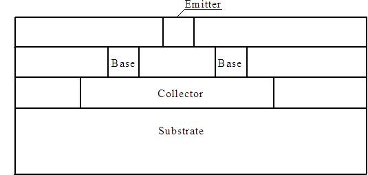
In this section we analyzed dynamic of redistribution of dopant and radiation defects in the considered heterostructure during their annealing by using calculated in the previous section relations. Typical distributions of concentrations of dopant in heterostructures are presented on Figs. 2 and 3 for diffusion and ion types of doping, respectively. These distributions have been calculated for the case, when value of dopant diffusion coefficient in doped area is larger, than in nearest areas. The figures show, that inhomogeneity of heterostructure gives us possibility to increase sharpness of p n- junctions. At the same time one can find increasing homogeneity of dopant distribution in doped part of epitaxial layer. Increasing of sharpness of p n-junction gives us possibility to decrease switching time. The second effect leads to decreasing local heating of materials during functioning of p n-junction or decreasing of dimensions of the p n-junction for fixed maximal value of local overheat. In the considered situation we shall optimize of annealing to choose compromise annealing time of infused dopant. If annealing time is small, the dopant has no time to achieve nearest interface between layers of heterostructure. In this situation distribution of concentration of dopant is not changed. If annealing time is large, distribution of concentration of dopant is too homogenous.
Fig.2. Distributions of concentration of infused dopant in heterostructure from Fig. 1 in direction, which is perpendicular to interface between epitaxial layer substrate. Increasing of number of curve corresponds to increasing of difference between values of dopant diffusion coefficient in layers of heterostructure under condition, when value of dopant diffusion coefficient in epitaxial layer is larger, than value of dopant diffusion coefficient in substrate
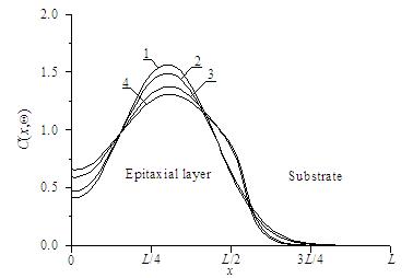
Fig.3. Distributions of concentration of implanted dopant in heterostructure
Advances in Materials Science and Engineering: An International Journal (MSEJ), Vol. 2, No. 1, March 2015
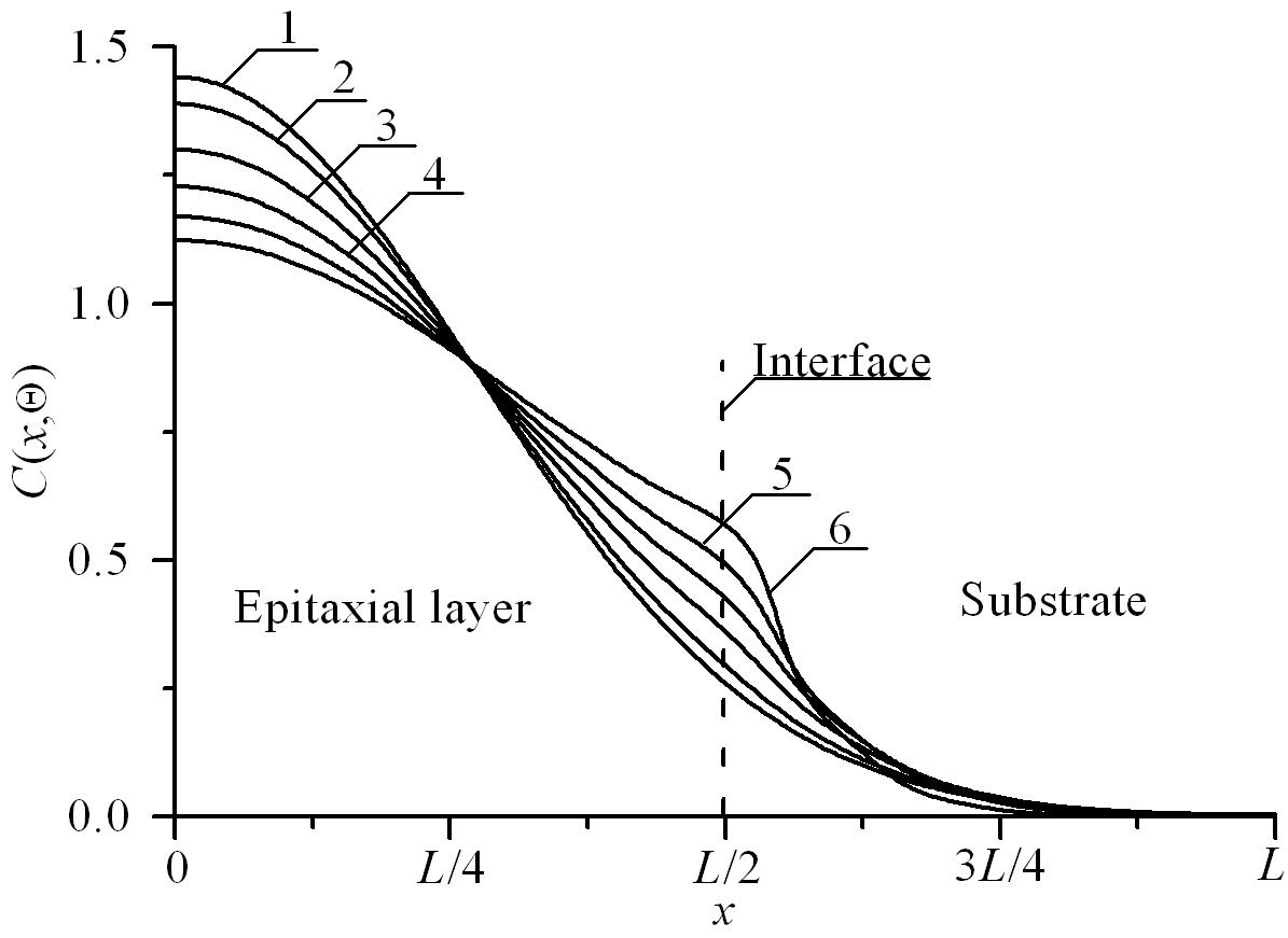
from Fig. 1 in direction, which is perpendicular to interface between epitaxial layer substrate. Curves 1 and 3 corresponds to annealing time Θ =0.0048(Lx 2+Ly 2+Lz 2)/D0. Curves 2 and 4 corresponds to annealing time Θ =0.0057(Lx 2+Ly 2+Lz 2)/D0. Curves 1 and 2 corresponds to homogenous sample. Curves 3 and 4 corresponds to heterostructure under condition, when value of dopant diffusion coefficient in epitaxial layer is larger, than value of dopant diffusion coefficient in substrate Ion doping of materials leads to generation radiation defects. After finishing this process radiation defects should be annealed. The annealing leads to spreading of distribution of concentration of dopant. In the ideal case dopant achieves nearest interface between materials. If dopant has no time to achieve nearest interface, it is practicably to use additional annealing of dopant. We consider optimization of annealing time framework recently introduced criterion [17,24-30]. Framework the criterion we approximate real distributions of concentrations by step-wise functions (see Figs. 4 and 5). Farther we determine optimal values of annealing time by minimization the following mean-squared error ()() []
Fig. 4. Spatial distributions of dopant in heterostructure after dopant infusion.
C ( x,Θ )
2 3 4 0 L
1
Curve 1 is idealized distribution of dopant. Curves 2-4 are real distributions of dopant for different values of annealing time. Increasing of number of curve corresponds to increasing of annealing time x
Fig. 5. Spatial distributions of dopant in heterostructure after ion implantation.
Advances in Materials Science and Engineering: An International Journal (MSEJ), Vol. 2, No. 1, March 2015
0.4
0.3
0.5 Θ D0 L-2 3
0.2
0.1
0.0
2 4 1
Curve 1 is idealized distribution of dopant. Curves 2-4 are real distributions of dopant for different values of annealing time. Increasing of number of curve corresponds to increasing of annealing time 0.00.10.20.30.40.5 a/L, ξ, ε, γ
Fig.6. Dependences of dimensionless optimal annealing time for doping by diffusion, which have been ob tained by minimization of mean-squared error, on several parameters.
0.12 Θ D0 L-2 3
0.08
0.04
2 4 1
0.00
Curve 1 is the dependence of dimensionless optimal annealing time on the relation a/L and ξ=γ= 0 for equal to each other values of dopant diffusion coefficient in all parts of heterostructure. Curve 2 is the dependence of dimensionless optimal annealing time on value of parameter ε for a/L=1/2 and ξ=γ = 0. Curve 3 is the dependence of dimensionless optimal annealing time on value of parameter ξfor a/L=1/2 and ξ=γ = 0. Curve 4 is the dependence of dimensionless optimal annealing time on value of parameter γfor a/L=1/2 and ε=ξ=0 0.00.10.20.30.40.5 a/L, ξ, ε, γ
Fig.7. Dependences of dimensionless optimal annealing time for doping by ion implantation, which have been obtained by minimization of mean-squared error, on several parameters.
Curve 1 is the dependence of dimensionless optimal annealing time on the relation a/L and ξ=γ= 0 for equal to each other values of dopant diffusion coefficient in all parts of heterostructure. Curve 2 is the dependence of dimensionless optimal annealing time on value of parameter ε for a/L=1/2 and ξ=γ = 0. Curve 3 is the dependence of dimensionless optimal annealing time on val-
Advances in Materials Science and Engineering: An International Journal (MSEJ), Vol. 2, No. 1, March 2015
ue of parameter ξfor a/L=1/2 and ξ=γ = 0. Curve 4 is the dependence of dimensionless optimal annealing time on value of parameter γ for a/L=1/2 and ε=ξ=0 where ψ(x,y,z) is the approximation function. Dependences of optimal values of annealing time on parameters are presented on Figs. 6 and 7 for diffusion and ion types of doping, respectively. Optimal value of time of additional annealing of implanted dopant is smaller, than optimal value of time of annealing of infused dopant due to preliminary annealing of radiation defects.
4. CONCLUSIONS
In this paper we consider an approach to manufacture more compact double base heterobipolar transistor. The approach based on manufacturing a heterostructure with required configuration, doping of required areas of the heterostructure by diffusion or ion implantation and optimization of annealing of dopant and/or radiation defects. The considered approach of monufactured the heterobipolar transistor gives us possibility to increase sharpness of p n-junctions framework the transistor. In this situation one have a possibility to increase compactness of the transistor.
Acknowledgments
This work is supported by the contract 11.G34.31.0066 of the Russian Federation Government, grant of Scientific School of Russia, the agreement of August 27, 2013 № 02.В.49.21.0003 between The Ministry of education and science of the Russian Federation and Lobachevsky State University of Nizhni Novgorod and educational fellowship for scientific research of Nizhny Novgorod State University of Architecture and Civil Engineering.
REFERENCES
1. V.I. Lachin, N.S. Savelov. Electronics. Rostov-on-Don: Phoenix, 2001.
2. A. Polishscuk. Modern Electronics. Issue 12. P. 8-11 (2004).
3. G. Volovich. Modern Electronics. Issue 2. P. 10-17 (2006).
4. A. Kerentsev, V. Lanin, Power Electronics. Issue 1. P. 34 (2008).
5. A.O. Ageev, A.E. Belyaev, N.S. Boltovets, V.N. Ivanov, R.V. Konakova, Ya.Ya. Kudrik, P.M. Litvin, V.V. Milenin, A.V. Sachenko. Semiconductors Vol. 43 (7). P. 897-903 (2009).
6. Jung-Hui Tsai, Shao-Yen Chiu, Wen-Shiung Lour, Der-Feng Guo. Semiconductors. Vol. 43 (7). P. 971-974 (2009).
7. O.V. Alexandrov, A.O. Zakhar'in, N.A. Sobolev, E.I. Shek, M.M. Makoviychuk, E.O. Parshin.Semiconductors. Vol. 32 (9). P. 1029-1032 (1998).
8. I.B. Ermolovich, V.V. Milenin, R.A. Red'ko, S.M. Red'ko. Semiconductors. Vol. 43 (8). P. 10161020 (2009).
9. P. Sinsermsuksakul, K. Hartman, S.B. Kim, J. Heo, L. Sun, H.H. Park, R. Chakraborty, T. Buonassisi, R.G. Gordon. Appl. Phys. Lett. Vol. 102 (5). P. 053901-053905 (2013).
10. J.G. Reynolds, C.L. Reynolds, Jr.A. Mohanta, J.F. Muth, J.E. Rowe, H.O. Everitt, D.E. Aspnes. Appl. Phys. Lett. Vol. 102 (15). P. 152114-152118 (2013).
11. K.K. Ong, K.L. Pey, P.S. Lee, A.T.S. Wee, X.C. Wang, Y.F. Chong, Appl. Phys. Lett. 89 (17), 172111-172114 (2006).
12. H.T. Wang, L.S. Tan, E. F. Chor. J. Appl. Phys. 98 (9), 094901-094905 (2006).
13. Yu.V. Bykov, A.G. Yeremeev, N.A. Zharova, I.V. Plotnikov, K.I. Rybakov, M.N. Drozdov, Yu.N. Drozdov, V.D. Skupov. Radiophysics and Quantum Electronics. Vol. 43 (3). P. 836-843 (2003).
14. I.P. Stepanenko. Basis of Microelectronics (Soviet Radio, Moscow, 1980).
15. A.G. Alexenko, I.I. Shagurin. Microcircuitry. Moscow: Radio and communication, 1990.
16. N.A. Avaev, Yu.E. Naumov, V.T. Frolkin. Basis of microelectronics (Radio and communication, Moscow, 1991).
17. E.L. Pankratov. Russian Microelectronics. 2007. V.36 (1). P. 33-39.
18. V.V. Kozlivsky. Modification of semiconductors by proton beams (Nauka, Sant-Peterburg, 2003, in Russian).
19. Z.Yu. Gotra, Technology of microelectronic devices (Radio and communication, Moscow, 1991).
Advances in Materials Science and Engineering: An International Journal (MSEJ), Vol. 2, No. 1, March 2015
20. P.M. Fahey, P.B. Griffin, J.D. Plummer. Rev. Mod. Phys. 1989. V. 61 № 2. P. 289-388.
21. V.L. Vinetskiy, G.A. Kholodar', Radiative physics of semiconductors. ("Naukova Dumka", Kiev, 1979, in Russian).
22. Yu.D. Sokolov. Applied Mechanics. Vol.1 (1). P. 23-35 (1955).
23. E.L. Pankratov. The European Physical Journal B. 2007. V. 57, №3. P. 251-256.
24. E.L. Pankratov. Int. J. Nanoscience. Vol. 7 (4-5). P. 187–197 (2008).
25. E.L. Pankratov, E.A. Bulaeva. Reviews in Theoretical Science. Vol. 1 (1). P. 58-82 (2013).
26. E.L. Pankratov, E.A. Bulaeva. Int. J. Micro-Nano Scale Transp. Vol. 3 (3). P. 119-130 (2012).
27. E.L. Pankratov. Nano. Vol. 6 (1). P. 31-40 (2011).
28. E.L. Pankratov, E.A. Bulaeva. J. Comp. Theor. Nanoscience. Vol. 10 (4). P. 888-893 (2013).
29. E.L. Pankratov, E.A. Bulaeva. Nanoscience and Nanoengineering. Vol. 1 (1). P. 7-14 (2013).
30. E.L. Pankratov, E.A. Bulaeva. Int. J. Micro-Nano Scale Transp. Vol. 4 (1). P. 17-31 (2014).
Authors:
Pankratov Evgeny Leonidovich was born at 1977. From 1985 to 1995 he was educated in a secondary school in Nizhny Novgorod. From 1995 to 2004 he was educated in Nizhny Novgorod State University: from 1995 to 1999 it was bachelor course in Radiophysics, from 1999 to 2001 it was master course in Ra diophysics with specialization in Statistical Radiophysics, from 2001 to 2004 it was PhD course in Radiophysics. From 2004 to 2008 E.L. Pankratov was a leading technologist in Institute for Physics of Micro structures. From 2008 to 2012 E.L. Pankratov was a senior lecture/Associate Professor of Nizhny Novgorod State University of Architecture and Civil Engineering. Now E.L. Pankratov is in his Full Doctor course in Radiophysical Department of Nizhny Novgorod State University. He has 105 published papers in area of his researches.
Bulaeva Elena Alexeevna was born at 1991. From 1997 to 2007 she was educated in secondary school of village Kochunovo of Nizhny Novgorod region. From 2007 to 2009 she was educated in boarding school “Center for gifted children”. From 2009 she is a student of Nizhny Novgorod State University of Architecture and Civil Engineering (spatiality “Assessment and management of real estate”). At the same time she is a student of courses “Translator in the field of professional communication” and “Design (interior art)” in the University. E.A. Bulaeva was a contributor of grant of President of Russia (grant № MK-548.2010.2). She has 59 published papers in area of her researches.