International Research Journal of Engineering and Technology (IRJET)

Volume: 09 Issue: 04 | Apr 2022 www.irjet.net
e ISSN:2395 0056
p ISSN:2395 0072
International Research Journal of Engineering and Technology (IRJET)
Volume: 09 Issue: 04 | Apr 2022 www.irjet.net
e ISSN:2395 0056
p ISSN:2395 0072
Sunil Manjhi
Singh Sehmi 2
,
2 M.Tech. Student, Dept. of Electrical Engineering, Shri Shankaracharya Group of Institutions, Bhilai CG, India
2 M.Tech. Student, Dept. of Electrical Engineering, Bhilai Institute of Technology, Durg, CG, India
***
Abstract To use renewable energy sources (RES) DC AC conversion is an essential key, thus to perform this operation we use inverters. Inverters are famous in the renewable field. As we use AC in our house and many places, but theenergyproducedbytherenewablesource is DC, therefore we need an inverter. Multilevel Inverters (MLIs) have become a lot of and more well liked in medium and highpower applications. this is often because of many inherent blessings of MLI over two level inverters like high quality output, smaller device ratings, and many other [1]
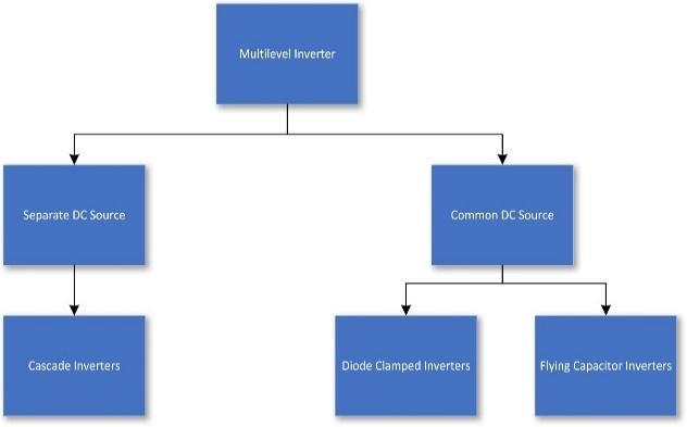
Because of less dV/dt tension, less voltage stress across powersemiconductorsystems,smallswitchingloss,and lower total harmonic distortion(THD) [1,2,3], MLI topologieshavelargelyoutplacedconventionaltwo level inverters. “The Inverter is the electrical device that converts direct current(DC) to alternate current(AC)”.
Whereas multilevel inverters convert DC to AC in multiple voltage levels and improve waveform of the voltage (make close to the sinusoidal waveform and reduceTHD).[4]
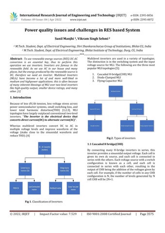
Multilevel inverters are used in a variety of topologies. The distinction is in the switching system and the input voltagesourceforMLI.Thefollowingarethethreemost popularMLItopologies[5]:
1. CascadedH bridge(CHB)MLI
2. Diode ClampedMLI
3. Flying CapacitorMLI
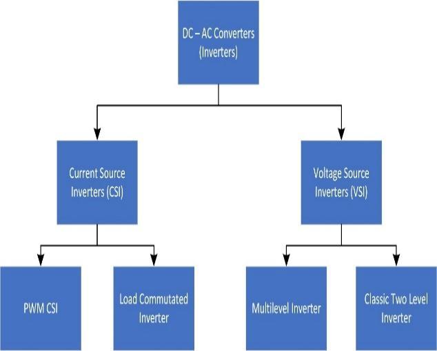
By connecting many H bridge inverters in series, this inverterprovidesasinusoidaloutputvoltage.Eachcellis given its own dc source, and each cell is connected in serieswiththeothers.Eachvoltagesourcewithaswitch configuration is known as a cell, and each cell is connected in series with each other, resulting in the outputofCHBbeingtheadditionofthevoltagesgivenby eachcell.Forexample,ifthenumberofcellsinanyCHB configuration is N, the number of levels generated by N cellCHBwillbe2N+1.
International Research Journal of Engineering and Technology (IRJET)
Volume: 09 Issue: 04 | Apr 2022 www.irjet.net
Here diodes are used to control and limit the voltage stress on the control device or switches. Let V voltage around each capacitor and switch, so the number of sources = (X 1), 2(X 1) switching devices, and (X 1)*(X 2)diodesarerequiredfóranXlevelinverter.
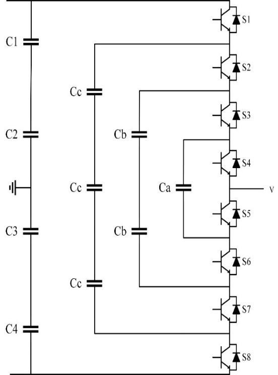
Inaa5 leveldiodeclampedmultilevel:
X=5
Therefore:
Switchused=2(X 1)=08 Diodeused=(X 1)*(X 2)=12
Capacitorused=(X 1)=04
AdiodeclampedMLIisshowninFig
©
e ISSN:2395 0056
p ISSN:2395 0072
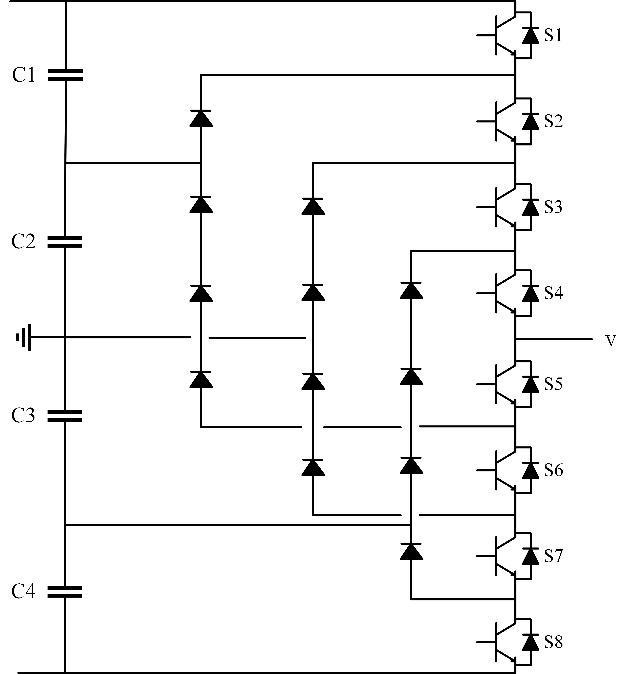
Capacitorsinthisinverterlimitthevoltageofthepower devices. The only difference between flying capacitor and diode clamped is that capacitors are employed to separate the input DC voltage. Let V represent the voltageinthevicinityofeachswitchandcapacitor.[6]
Xlevelflyingcapacitorinverterneeds
Switchused:(2X 2)
Capacitorused:(X 1)
value:
The reliability of the topology of the MLI has the principal importance as the power semiconductor switches used in the architecture of the topology of the MLI are vulnerable. In light of the applications such as industrial manufacturing, the main operation is based upon induction motors and their inverter for process control.
To protect the inverter and induction machine(motor), traditional protection systems typically comprise of passive devices such as circuit breaker(CB), overload relays, and fuses. When a failure occurs[7], the protection devices separate the power sources from the multilayer inverter, resulting in the process being interrupted. Manufacturing equipment can cost thousands or hundreds of thousands of dollars per hr during a period of malfunction in power switches,
International Research Journal of Engineering and Technology (IRJET)
Volume: 09 Issue: 04 | Apr 2022 www.irjet.net
therefore fault tolerant operation is required to ensure continuous operation and prevent damage to the inverter.[9]
Inarecentsurveyoveranamountof200productsfrom 80 various companies, it is found that the power switches are responsible for 38% of failure in an inverter. The failure in power semiconductor switches canbeclassifiedintotwotypesnamelyopencircuit(OC) faultandshortcircuit(SC)fault.[7]
The SC failure causes the faulty switch to conduct even whenitisturnedoff,potentiallycausingashoot through condition in the DC source or capacitor. This problem can be avoided by placing fuses in the conducting path, whichwillconvertthefaultbacktoanOCfault.
In the situation of an inverter with an induction motor, anOCfaultwillresultinanunbalancedconditionofload voltage and load current. If an induction motor is supplied with imbalanced voltage and current for an extendedperiodoftime,theinductionmotormaysuffer critical damage due to high temperature. This could cause severe damage to the induction motor's winding andcausetheentiresystemtoshutdown.Asaresult,an opencircuitfault tolerantmultilevelinverterisrequired toensuretheinverter'sproperoperationwhilelowering theexpenseofadditionalprotectivedevices.
The OC fault conditions on respective switches of each leg of Flying Capacitor or Diode Clamped causes the unbalancing of the capacitor voltage and ultimately results in the loss of a generation of voltage levels. This major issue will result in the failure of the healthy operation of both topologies. With this concern, the analysis is performed on open circuit fault on each switchofbothtopologies.
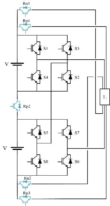
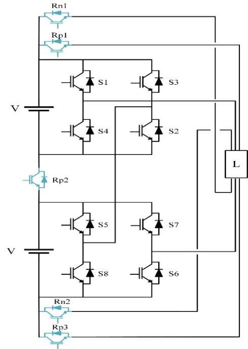
A schematic diagram of the three phase 5 level MLI structure is shown in Figure 1, and Phase A of the proposed structure is shown in Figure 2. The proposed FT MLI consists of 8 unidirectional switches per phase and 5 redundant path switch, which includes 2 DC source voltage V1 and V2. The 14 switching state configurationsofproposeMLIarelistedinTable1.
e ISSN:2395 0056
p ISSN:2395 0072
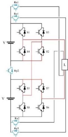
Fig 7.Phase Aofproposed5 levelMLIstructure
Table 1 Switchingstatesofthestudied5 levelMLI
0utput Voltage Switchi ngState S1 S2 S3 S4 S5 S6 S7 S8 100V State1 ON ON OF F OF F ON ON OF F OF F 50V State2 ON ON OF F OF F ON OF F ON OF F State3 ON ON OF F OF F OF F ON OF F ON State4 ON OF F ON OF F ON ON OF F OF F State5 OF F ON OF F ON ON ON OF F OF F 0V State6 ON OF F ON OF F ON OF F ON OF F State7 OF F ON OF F ON OF F ON OF F ON State8 ON ON ON OF F OF F ON OF F ON State9 OF F OF F OF F ON ON OF F ON OF F 50V State10 OF F OF F ON ON ON OF F ON OF F State11 OF F OF F ON ON OF F ON OF F ON State12 ON OF F ON OF F OF F OF F ON ON State13 OF F ON OF F ON OF F OF F ON ON 100V State14 OF F OF F ON ON OF F OF F ON ON
International Research Journal of Engineering and Technology (IRJET)
Volume: 09 Issue: 04 | Apr 2022 www.irjet.net
Table 2 is presented the lost switching states due to faults in the switches , fault in each switch effects the certainswitchingstatesandtocompensatethatweused the redundant switches with ensure the proper and affectiveworkingofFT MLIduringtheOpenCircuitfault ,loststate isreplaced by thedifferent switchingstateof theredundantpathshowninthetable3,althoughstress oneachswitchesincreasedduetothefault.Beforefault, proposedtopology work asa normal CHBinverter,until and unless there is fault, fault activate the redundant switch.
Under normal condition proposed topologyworkslikea simple CHB and give output of level shifted five level output. But under faulty condition redundant path will beactivated.
Below figures represents the working of the redundant pathduringthefaultycondition.
State1 State2 State3
State4 State5
Fig 8.Currentpathwaysandconductingpathwaysof proposedMLIfor5 level
e ISSN:2395 0056
p ISSN:2395 0072
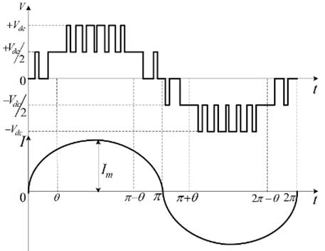
For better understanding, Figure 9 represents a complete cycle of the 5 level o/p voltage and current waveform.
Fig 9.Completecycleofthefive leveloutputvoltageand currentwaveform
.Table 2 Unavailable states in case of any single switch OCfaultinMLI
FailedSwitch Effected Switching State Output VoltageLevel
S1 State1,2,3,4,6,8,12 100V
S2 State1,2,3,5,7,9,13 100V
S3 State4,6,8,10,11,12,14 100V
S4 State5,7,9,10,11,13,14 100V
S5 State1,2,4,5,6,9,10 100V
S6 State1,3,4,5,7,8,11 100V
S7 State2,6,9,10,12,13,14 100V
S8 State3,7,8,11,12,13,14 100V
Table 2 has shown that if any one of the switches encountersafailurethenitseffectedstateswillbe.
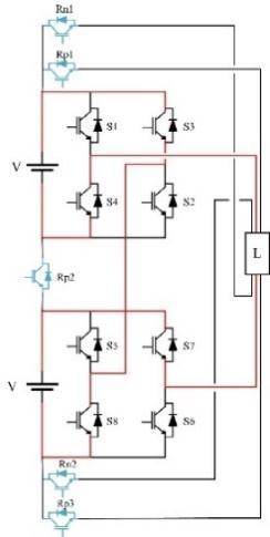
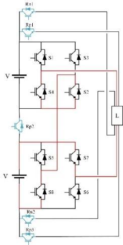
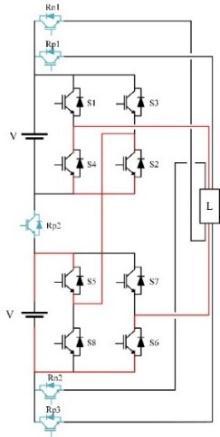
The conventional topology requires the FT feature obstructing the output for faults in the switches. The authors have addressed the issue and some modifications in the existing single phase MLI to incorporate inherent FT capability. An additional switch Rp1, Rp2, Rp3 and Rn1, Rn2 has been added to the conventional MLI, to obtain the modified single phase (5 level)MLIwithFTfeatureasshowninFigure10
© 2022, IRJET | Impact Factor value: 7.529 | ISO 9001:2008 Certified Journal
Page3578
International Research Journal of Engineering and Technology (IRJET)
Volume: 09 Issue: 04 | Apr 2022 www.irjet.net
Fig 10.TheProposedFT MLIstructure
The valid switching status of the proposed FT MLI in case of single switch faulty conditions is presented in Table3.[9]
Table 3 Availableoutputvoltagelevelsoftheproposed FTMLIincaseofsingleswitchfailure
FailedSwitch ActiveSwitches OutputVoltage
S1 Rp1,Rp2,Rp3 100
S2 Rp1,Rp2,Rp3 100
S3 Rp2,Rn1,Rn2 100
S4 Rp2,Rn1,Rn2 100
S5 Rp1,Rp2,Rp3 100
S6 Rp1,Rp2,Rp3 100
S7 Rp2,Rn1,Rn2 100
S8 Rp2,Rn1,Rn2 100
ThesimulationresultsoftheproposedFT MLIstructure arediscussed.Toverifythestructureunderbefore fault, faulty, and after fault conditions, the proposed FT MLI simulatedusingMATLAB Simulinksoftware.Thecurrent study employs a multicarrier phase opposition dispositionPWM(POD PWM)schemewithlevelshifting (LS PWM). The gate signal pulses for triggering ON the power switching devices are generated using the LS PWMmodulation [10]
Impact Factor value: 7.529
e ISSN:2395 0056
p ISSN:2395 0072
In this multicarrier SPWM strategy, the 4 trianguler carrier signal are compare to the modulating sinusoidal reference signal for required gate pulses. The modulation index of 0.85 and the modulating wave frequency(fm) 50Hzhasbeenusedforbothsimulation andexperimentation.[11]
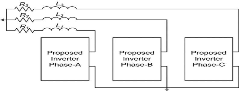
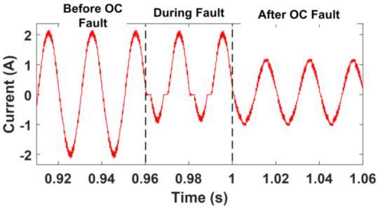
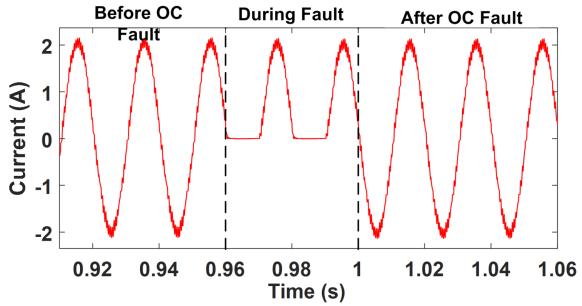
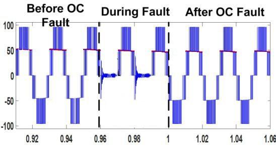
To examine the performance of the proposed FT MLI structureissimulatedusing MATLAB Simulink,whichis alsodemonstratedexperimentallythroughanRLloadis taken with R = 20 ohm & L = 20 miliH The simulation resultandwaveformsareshowinthefigure11&12.
InputDCSupplyVoltageVs=100V
Modulationindex=0.85
Switchingfrequency(fs)=2000kHz
LoadvaluesR=20Ω,L=20mH
Figure 11 and Figure 12 shows the output voltage and load current waveforms for OC fault in switches, respectively. The output waveform are maintained due totheredundantpathsavailableforthesefaults
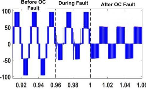
Fig 11. Simulationoutputvoltageandloadcurrent waveformunderfault
International Research Journal of Engineering and Technology (IRJET)
Volume: 09 Issue: 04 | Apr 2022 www.irjet.net
Fig 12.Simulationoutputvoltageandloadcurrent waveformunderfault
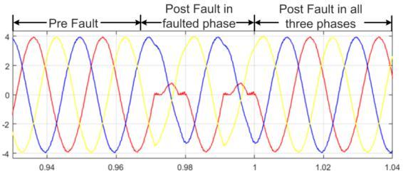
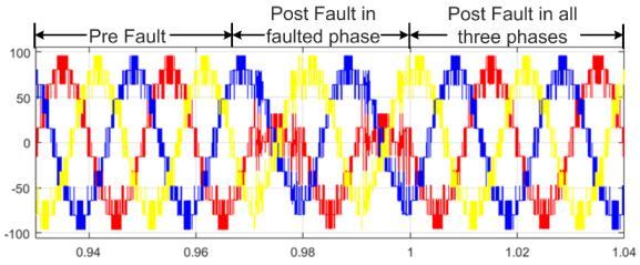
Similar results are obtained in the case of the three phase structure of the proposed 5 level MLI. Figure 13 shows the phase voltages of the proposed FT MLI structure for an open circuit fault in the switch . Figure 13(b) and Figure 13(c) shows the line to line voltages andloadcurrentrespectively.
(c)
(a)
(b)
e ISSN:2395 0056
p ISSN:2395 0072
Fig 13 Simulationoutput resultsfortheproposedFault
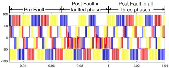
Tolerant MLI structure in switch S1 under Pre fault, faulty, post fault states (a) Line voltages, (b) Phase voltages,(c)Phasecurrents
Notably, the result clearly presented the proposed FT MLI structure have the FT feature against OC faults that isanysingleswitchfailure.Theoutputvoltgisdecreased from 5 level to 3 level & peak magnitude is halved. Simultaneously, a similar effect shows on the load current.
TopreventOCfaultsinswitcheswithasmall numberof devices, this work provides a single phase and three phase FT MLI structure with numerous redundant levels. In addition, the suggested FTMLI modulating technique has been tested in all modes of before fault, faulty, and after fault. According to a comparison, the presentedFT MLIstructurecontainsfewermoredevices than recently published fault tolerant topology, but it ensure appropriate functioningwhen the system is faulty. Finally, various simulations show that the suggested MLI structure can operate in a fault tolerant way.
[1] Dhananjay Kumar, Rajesh Kumar Nema, Sushma Gupta. "Investigation of fault tolerant capabilities of some recent multilevel inverter topologies", International Journal of Electronics, (2021) pp 1957 1976
[2]J.Rodriguez,S.Bernet,P.K.Steimer,andI.E.Lizama, "A survey on neutral point clamped inverters." IEEE transactions on Industrial Electronics 57,no.7(2009)pp. 2219 2230.
[3] K.K. Gupta, A. Ranjan, P. Bhatnagar, L.K. Sahu, S. Jain,"Multilevel inverter topologies with reduced device count:Areview." IEEE transactions on Power Electronics 31,no.1(2015)pp.135 151.
International Research Journal of Engineering and Technology (IRJET)
Volume: 09 Issue: 04 | Apr 2022 www.irjet.net
[4] Alamri, Basem, and Mohamed Darwish. "Power loss investigation in HVDC for cascaded H bridge multilevel inverters (CHBMLI)", 2015 IEEE Eindhoven PowerTech, (2015).
[5] Bana, P. R., Panda, K. P., Naayagi, R. T., Siano, P., & Panda,G."Recentlydevelopedreducedswitchmultilevel inverter for renewable energy integration and drives application: topologies, comprehensive analysis and comparative evaluation." IEEE access 7 (2019): 54888 54909.
[6] Sambasivam Rajalakshmi, Dr. Parthasarathy Rangarajan. "Investigation of modified multilevel inverter topology for PV system", Microprocessors and Microsystems,(2019)pp.102870
[7] Surin Khomfoi. Leon M Tolbert " Fault diagnostic systemforamultilevelinverterusinganeuralnetwork", IEEE Transactions on Power Electronics, 5/2007 1062 1069
[8]V.V.S.PradeepKumarandB.G.Fernandes,"AFault TolerantSingle PhaseGrid ConnectedInverterTopology With Enhanced Reliability for Solar PV Applications," in IEEE Journal of Emerging and Selected Topics in Power Electronics,vol.5,no.3,Sept.2017pp.1254 1262
[9] E. Bikdeli and M. R. Islam, "A New Hybrid Fault Tolerant Converter Based on Five Level Active Neutral Point Clamped Inverter," 2021 IEEE 6th International Conference on Computing, Communication and Automation(ICCCA),2021,pp.714 719
[10]N.K.Dewangan,S.Gupta,andK.K.Gupta,"Approach to synthesis of fault tolerant reduced device count multilevel inverters (FT RDC MLIs)." IET Power Electronics 12,no.3(2018):476 482.
[11] M. Jalhotra, H. Allamsetty and L. Kumar, "A single phasefaulttolerant multilevel InverZter topology," 2017 2nd IEEE International Conference on Recent Trends in Electronics, Information & Communication Technology (RTEICT),2017,pp.1022 1026.
© 2022,
e ISSN:2395 0056
p ISSN:2395 0072
Impact Factor value: 7.529
9001:2008