A printed circuit board (PCB), is used to mechanically support and electrically connect electronic components using conductive pathways, or signal traces etched from copper sheets laminated onto a non conductive substrate anditisalsonon conductiveforundefinedpaths.Thebelow PCB is fabricated with FR4 base material that is flame retardantupto140c.Easy EDAsoftwareisusedtodesign PCB that combines component placement and routing to define electrical conductivity on a manufactured circuit board.
International Research Journal of Engineering and Technology (IRJET) e ISSN: 2395 0056 Volume: 09 Issue: 03 | Mar 2022 www.irjet.net p ISSN: 2395 0072
2. DESIGN PROCEDURE
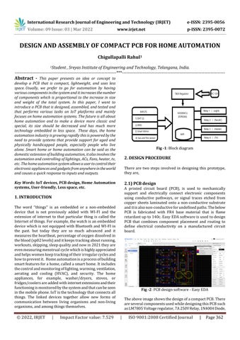
TheaboveimageshowsthedesignofacompactPCB.There areseveralcomponentsusedwhiledesigningthisPCBsuch asLM7805Voltageregulator,7A250VRelay,1N4004Diode,
Abstract This paper presents an idea or concept to develop a PCB that is compact, lightweight, and uses less space. Usually, we prefer to go for automation by having various components in the system and it increases thenumber of components which is proportional to the increase in size and weight of the total system. In this paper, I want to introduce a PCB that is designed, assembled, and tested and that performs various tasks on IoT platforms and mainly focuses on home automation systems. The future is all about home automation and to make a device more classic and special, its size should be decreased and has much more technology embedded in less space. These days, the home automation industry is growing rapidly this is powered by the need to provide systems that provide support for aged and physically handicapped people, especially people who live alone. Smart home or home automation can be said as the domestic extension of building automation, it alsoinvolves the automation and controlling of lightings, ACs, Fans, heater, tv, etc. The home automation systemallowsausertocontroltheir electronic appliances and gadgetsfromanywhereintheworld and causes a quick response to inputs and outputs.
1. INTRODUCTION
Key Words: IoT devices, PCB design, Home Automation systems, User friendly, Less space, etc.
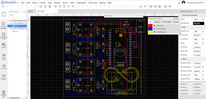
The word ‘’things’’ is an embedded or a non embedded device that is not previously added with WI FI and the extension of internet to that particular thing is called the Internetofthings.Forexample,thewatchisanembedded device whichisnotequippedwithBluetoothand WI FIin the past. but today they are so much advanced and it measurestheheartbeat,percentageofoxygendissolvedin theblood(sp02levels)anditkeepstrackingaboutrunning, workouts,skipping,sleepqualityandnowin2021theyare evenmeasuringmenstrualcyclewhichishighlyappreciated andhelpswomenkeeptrackingoftheirirregularcyclesand howtopreventit. Homeautomationisaprocessofbuilding smartfeaturesforahome,calledasmarthome.Itincludes thecontrolandmonitoringoflighting,warming,ventilation, aerating and cooling (HVAC), and security. The home appliances, for example, washer/dryers, stoves, or fridges/coolersareaddedwithinternetextensionsandtheir functioningismonitoredbythesystemandthatcanbeseen inthemobilephone.IoTisthetechnologythatconnectsall things. The linked devices together allow new forms of communication between living organisms and non living organisms,andamongthingsthemselves. Blockdiagram
Fig 1:
There are two steps involved in designing this prototype, theyare, 2.1) PCB design
Fig 2:PCBdesignsoftware EasyEDA
Journal | Page362
DESIGN AND ASSEMBLY OF COMPACT PCB FOR HOME AUTOMATION Chigullapalli Rahul1 1Student , Sreyas Institute of Engineering and Technology, Telangana, India. ***
© 2022, IRJET | Impact Factor value: 7.529 | ISO 9001:2008 Certified

International Research Journal of Engineering and Technology (IRJET) e ISSN: 2395 0056 Volume: 09 Issue: 03 | Mar 2022 www.irjet.net p ISSN: 2395 0072
© 2022, IRJET | Impact Factor value: 7.529 | ISO 9001:2008 Certified Journal | Page363
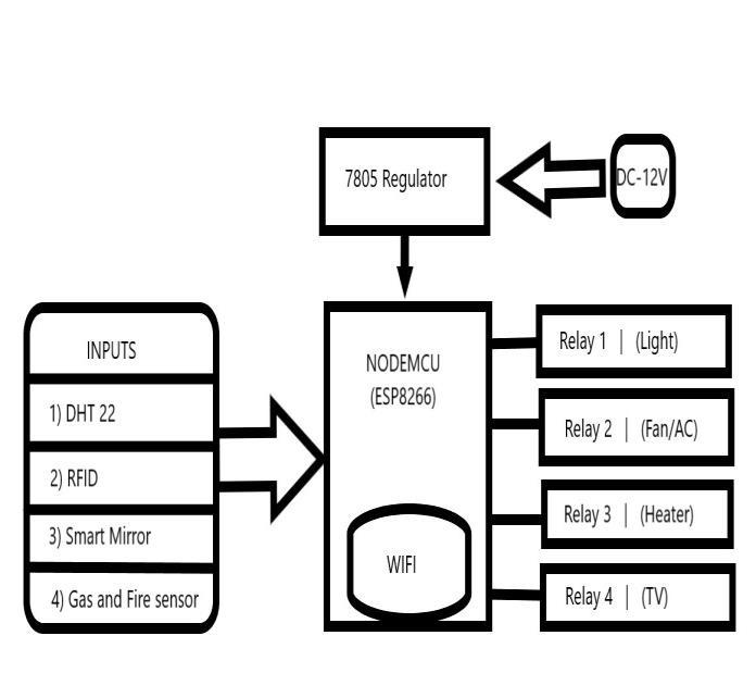
Fig 3:PCBdesigndescribingslotstodifferentsensors
Thesoftwareshowsthesimulationofthedesignanditgives anaccurateoutputofthepartthathastobemanufactured. PCBsimulationsarethecapturephaseofadesignandthat processhelpsindesigningandverifyingthemechanicaland electricalaspectsofthepresentdesign.Theyareusefulfor checking clearances and the alignment of the connectors. Mostimportantly,wecanabletoseetheoverlappingoftop andbottomlayerswhichmaycausethefailureofPCB,and sometimesitmayalsoresultinconnectingthepositiveand negativevoltagesaswell.So,itisimportanttoverifyallthe layersandtheirroleinoverlappingbeforeitisgiventothe productionandfabricationprocess.EasyEDAisaweb based toolthatenablesengineerstodesignanddevelopthePCB A) The PCB is manufactured and the below picture showsthemodelbeforeassembling.
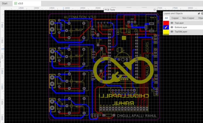
Fig 5:Manufacturedmodel B) The PCB is assembled with the required componentsinvolvedinthedesignsoftware.
The left PCB is only used for turning on the electrical appliances. Meanwhile, the PCB on right is used to access different types of input data provided by the digital and analogsensorsprovidedonthePCB.ESP8266containsonly oneanaloginput,soitdoesnottakemanyanaloginputsand processthedata.Amultiplexerisusedtoprocessdifferent kinds of analog signals and sends the information to the analogpinontheNode MCUboard.Someoftheresistorsare solderedonthetoplayerofthePCBandothercomponents are soldered under the bottom layer. Every component is electrically tested before assembling them onto the PCB board.
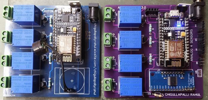
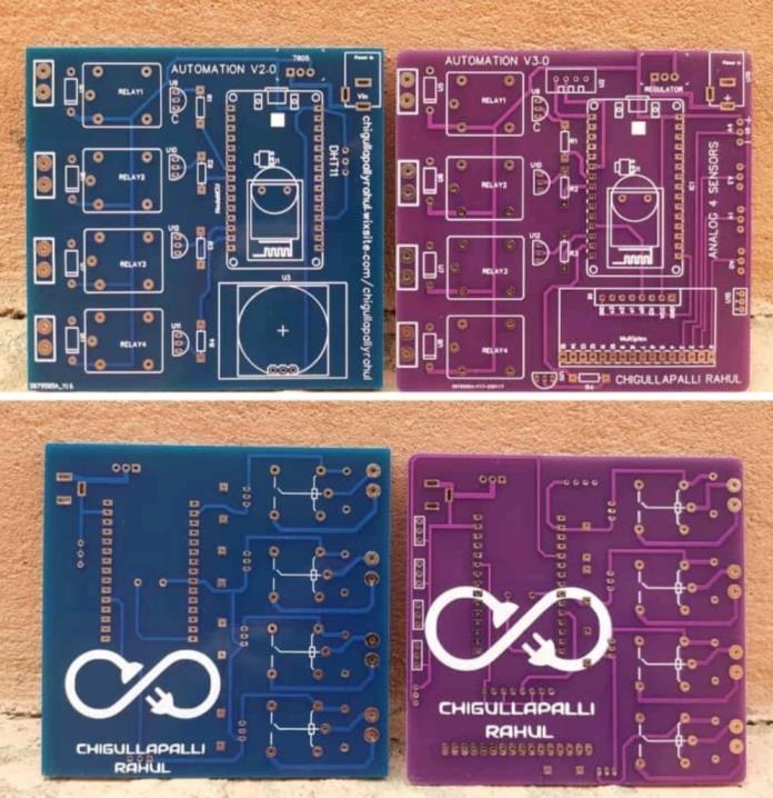
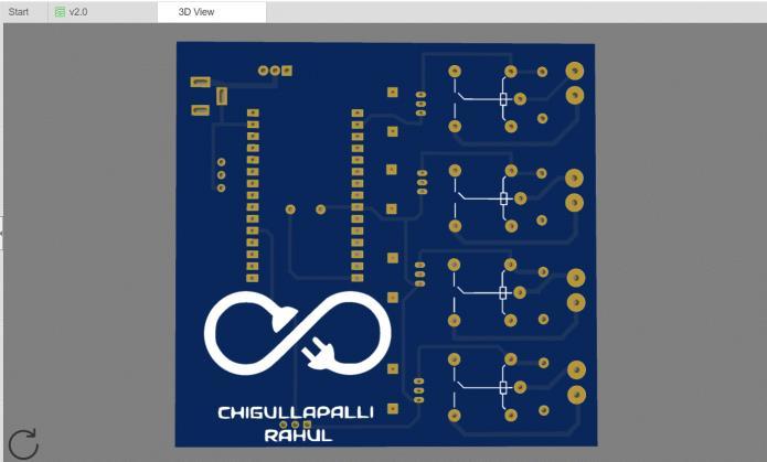
Fig 4:3Dsimulation
Fig 6:Assembledmodel
BC547 Transistors, Multiplexer, ESP8266, and a DC 12V socket for power supply. The designed PCB is given to manufacturingand itisfabricatedwithFR4base material which is a glass fiber epoxy laminate. It is the most commonly used PCB material. FR 4 is used widely for printedcircuitboards.Athinlayerofcopperfoilisusually laminatedtooneorbothsidesofanFR 4glassepoxypanel. Thesearecommonlyreferredtoascopper cladlaminates. Thecopperthicknessorcopperweightisvariable.
2.2) Outer case design using Fusion 360 Fig 7:CADmodel(bottompart)
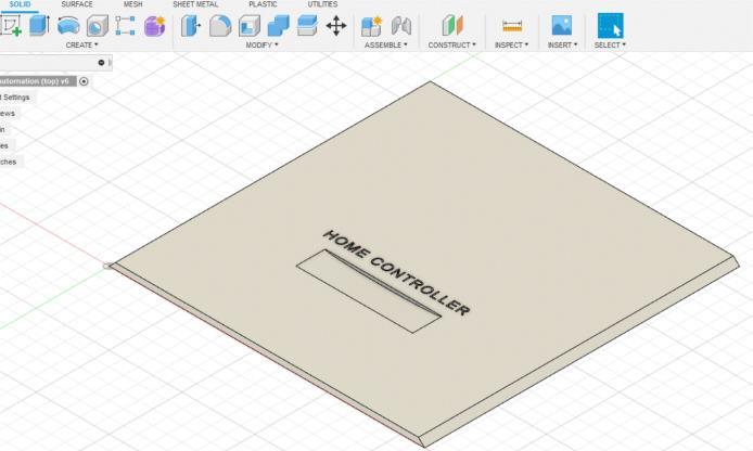
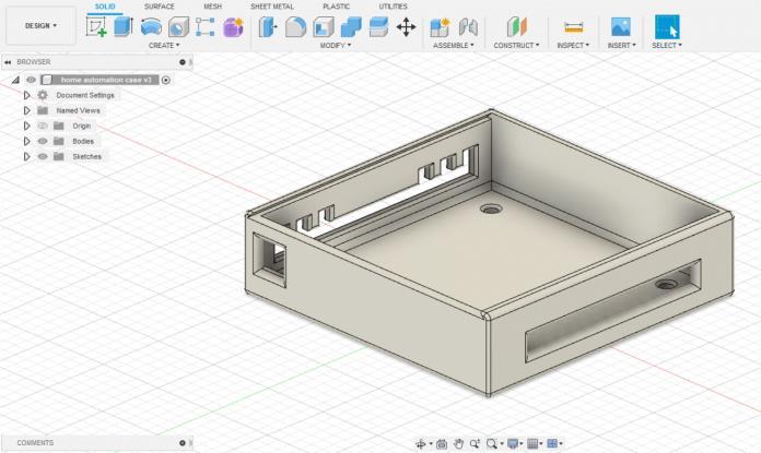
Fig 8:CADmodel(Toppart)
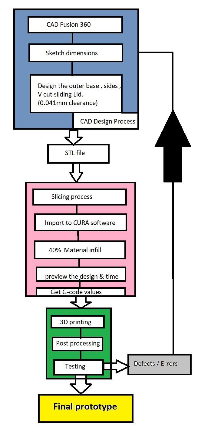
Support structures:Asupportstructureisatechniquedone duringtheslicingprocessthathelpsinsupportingthebuild partofmaterial.Inabsenceofthisfeature,thenextlayerwill notbedepositedoverthepreviouslayerwhichresultsinthe error.Thelayerwillnotbuildontheadjacentlayerandthe extruderkeepsonejectingthematerialintheair. Many3D printing processes create the object layer by consecutive layer,downtoupinascendingorderoflayernumbers,with the layer under construction being deposited over the previousone.
Fig 9:SlicingtheCADmodel
Thetoppartisgivenwithanellipsecuttoslideitduring openingandclosingthelid.
Theslicingsoftwareisacomputersoftwareusedinmany3D processes. It is useful in converting the information to somethingwhichisunderstandabletothe3Dprinter.Cura slicing is a powerful, open source slicing engine, this softwareisbuiltwiththehelpofusercontributions. slicer softwareinitiallydividestheobjectasabunchofflatlayers, and these layers are linear movements of the 3D printer extruder.Allthesemovements,togetherwithsomespecific printer commands like the ones to control the extruder temperatureorbedtemperature,arefinallywrittenintheg codefilethatisunderstoodonlybythe3dprinter. Infill: solidobjectsneedalargeamountofmaterialwhichis calledfilament.Afilamentcanbeinsolidform,liquidform andpowderformdependingupontheprocessperforming fortheparticulartask.Fortoys,ABS(acrylonitrilebutadiene styrene) plastic can be used which is a plastic wire solid materialandprinttimeincreaseswiththeincreaseofinfill percentages. In this project 40% of infill is used, which is enough to build beautiful and strong layers of the model. Also,polylacticacid(PLA)iswidelyusedbecauseitisbio degradableinnature.Theslicerhastheinbuiltcapabilityto convert solid volumes to hollow ones automatically, that savescostsandtime.
Volume: 09 Issue: 03 | Mar 2022 www.irjet.net p ISSN: 2395 0072
© 2022, IRJET | Impact Factor value: 7.529 | ISO 9001:2008 Certified Journal | Page364
The dimensions and requirements are taken into consideration. It's a 90*90 mm PCB. So, it should have a spacingof10mmonbothsideswhichresultsin110mmof the plastic case layer. The 20mm gap is given to have adequate airflow to the PCB and thereby it exchanges the heattosurroundingair.Toavailmoreairflowintothebox, thedesignisgivenwithholesandslots.IusedFusion360 CADsoftwaretodesigntheoutercase(box)andsimulatedit insidethesoftwarewiththehelpoftherenderfeature.
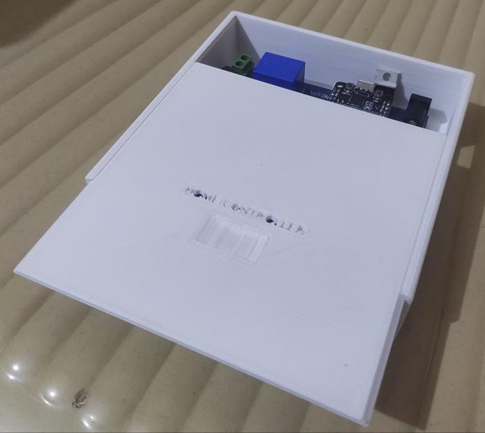
Fig 10:3Dprintedslidingcase
International Research Journal of Engineering and Technology (IRJET) e ISSN: 2395 0056
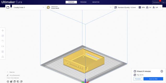
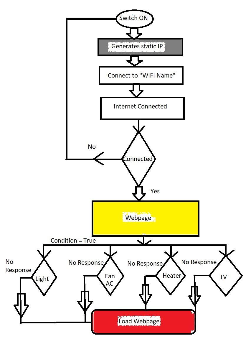
Figure12illustratesthesequenceofactivitiestakingplacein betweentheESP8266anditswebserver.Initially,theNode MCU generates a static IP address which is mandatory to access the webpage contents. Once it is connected to the WIFI,itwillloadthewebpagecontainingtherelays.Those relays get activated when the corresponding button is pressedandthehtmlrequestisacceptedbytheboardandit sends a command to the associated relay. The microcontroller sends the current and it turns on the electromagneticrelay.Anyelectronicapplianceconnectedto the relay gets turned on. For example, if the heater is connectedtoanactivatedrelay,thenheatergetsswitchedon andheatsthe waterbeyond room temperatureandit will automatically cut off its power supply when a certain temperatureconstraintisreached.
3. IMPLEMENTATION
© 2022, IRJET | Impact Factor value: 7.529 | ISO 9001:2008 Certified Journal | Page365
Fig 12:Activitychart
International Research Journal of Engineering and Technology (IRJET) e ISSN: 2395 0056 Volume: 09 Issue: 03 | Mar 2022 www.irjet.net p ISSN: 2395 0072
As soon as the material is printed, it will be sent to post processingwhichmakestheprocesssimplerforremoving the unwanted materials and giving the prototype a good surfacefinish.Ifthereareanyerrorsfound,someofthem can be minimized and other errors cannot be accepted, which in turn, the cycle repeats until it achieves a final prototypewithoutanyscalableerrorsanddefects.
Fig 11:Processfor3Dprinting
and
International Research Journal of Engineering Technology (IRJET) e ISSN: 2395 0056 Volume: 09 Issue: 03 | Mar 2022 www.irjet.net p ISSN: 2395 0072
© 2022, IRJET | Impact Factor value: 7.529 | ISO 9001:2008 Certified Journal | Page366
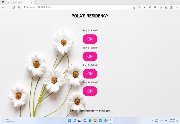
Fig 13:AccessingthewebpageinMobile
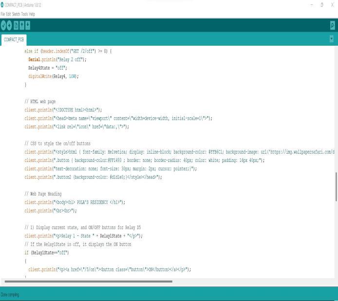

4. SOFTWARE Fig -14:ArduinoIDE ArduinosoftwareisusedtocodeESP8266Board.Basically, this board does not have any programmer/ software to uploadthecode.Duetothisreason,Arduinoisusedtowrite the sketch and upload the code to ESP8266. But, before writingthesketch,oneshouldbeabletopastethereference link of ESP in the file preferences bar and continue to downloadNode MCUboardsfromtheboardsmanagerand othersufficientlibrariesthatneedtobeinstalledinorderto compile the code. Without sufficient libraries and header files,theprogramwillnotcompile. The HTML file format is understandable to computers to createwebpagesandgetresponses.Thesefilesmustcontain anextensionlikefile.htmorfile.html.Forexample,toaccess myprogramfilewhichisstoredinalocalcomputer.Thenit is required to open Homeautomation.html to display the webpageofthisproject.Thesemarkupscontaininstructions toredirectitselftoabrowserandperformitstaskaswritten intheHTML. Thisplatformalsoincludes manyfeaturessuchasinclude preferences,addlibraries,createyourownsketch,cut,copy, paste,modify,showingbracesetc.Onlyonebuttonisenough tocompilethewholecodeandasingleclickisrequiredto uploadthecodetotheboard.TheNode MCUboardisalow costandpowerfuldevice,ItconnectstotheWIFIinasecond andresponsetimeisverylessandefficientindeliveringthe output
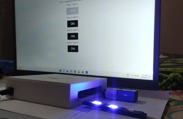
Thewebpagedisplaysthecurrentstateoftherelayandits working condition with the electrical appliances. The webpage is made with html and added some of the CSS features to make it look beautiful and glossy. It is an embeddedsystemespeciallymadeforaccessingthehome contentsanditcanworkaroundtheWIFIrange.AnMDNS Server is also established and it is named as “HomeAutomation.local/”. This is the process of giving a webpageanamefromitsstaticIPaddress.
UsingESP8266asthemicrocontrolleranditscapabilityto connect over the internet is really fascinating for the developerswhoworkonWIFIextensionstochangeathing fromNonIoTtoIoTbackground.Successfullycontrolledthe home appliances using ‘’Compact PCB’’ which is only 11*11Cm(110*110mm)insizeandfitseverywhere.
[1] Smart GSM Based Home Automation SystemRozita Teymourzadeh, CEng, Member IEEE/IET, Salah Addin Ahmed,KokWaiChan,andMokVeeHoongFacultyof Engineering,Technology&BuiltEnvironment. [2] A. C. Jose and R. Malekian, “Smart home automation security:Aliteraturereview,”SmartComputingReview, vol.5,no.4,pp.269 285,2015.
REFERENCES
[3] Volume 2, Issue 12, December 2014 International JournalofAdvanceResearchinComputerScienceand ManagementStudiesResearchArticle/SurveyPaper/ CaseStudy. BIOGRAPHY Chigullapalli Rahul, B.Tech Final year Havingstudent.interested in Electronics, ElectromechanicsandAutomation I'vedonemorethan50projectson the Arduino platform by myself. Myinterestsaretakingaproblem statement and finding suitable solutions in a low cost method Watchapproach.this project on YouTube : https://youtu.be/d1_4wOmTTes

6. CONCLUSION Inthispaper,itismainlyfocusedonthedesignandassembly ofthevariouscomponentsontothePCB.Theprototypesize has decreased rapidly when compared to all other home automationwireddevices.Therearenowiresatallinthis deviceanditisfullyoperatedonWIFI.Thehomeautomation madeoutof“CompactPCBdesign”hasbeenexperimentally proven to work satisfactorily by connecting various electricalappliancestoit.
Fig 16:AccessinPC(HTML)
© 2022, IRJET | Impact Factor value: 7.529 | ISO 9001:2008 Certified Journal | Page367
International Research Journal of Engineering and Technology (IRJET) e ISSN: 2395 0056 Volume: 09 Issue: 03 | Mar 2022 www.irjet.net p ISSN: 2395 0072
5. RESULTS
Fig -15:AccessinPC(CSS)